US7607790B2 - Backlighting apparatus and manufacturing process - Google Patents
Backlighting apparatus and manufacturing process Download PDFInfo
- Publication number
- US7607790B2 US7607790B2 US11/640,587 US64058706A US7607790B2 US 7607790 B2 US7607790 B2 US 7607790B2 US 64058706 A US64058706 A US 64058706A US 7607790 B2 US7607790 B2 US 7607790B2
- Authority
- US
- United States
- Prior art keywords
- circuit board
- thermal
- backlight module
- backlight
- module according
- Prior art date
- Legal status (The legal status is an assumption and is not a legal conclusion. Google has not performed a legal analysis and makes no representation as to the accuracy of the status listed.)
- Active
Links
- 238000004519 manufacturing process Methods 0.000 title claims abstract description 26
- 239000012792 core layer Substances 0.000 claims abstract description 35
- 239000004020 conductor Substances 0.000 claims abstract description 7
- 239000002344 surface layer Substances 0.000 claims abstract description 7
- 239000000463 material Substances 0.000 claims description 31
- 238000000034 method Methods 0.000 claims description 23
- 230000008569 process Effects 0.000 claims description 20
- 238000009423 ventilation Methods 0.000 claims description 13
- RYGMFSIKBFXOCR-UHFFFAOYSA-N Copper Chemical compound [Cu] RYGMFSIKBFXOCR-UHFFFAOYSA-N 0.000 claims description 11
- 229910052782 aluminium Inorganic materials 0.000 claims description 11
- XAGFODPZIPBFFR-UHFFFAOYSA-N aluminium Chemical compound [Al] XAGFODPZIPBFFR-UHFFFAOYSA-N 0.000 claims description 11
- 239000010949 copper Substances 0.000 claims description 11
- 229910052802 copper Inorganic materials 0.000 claims description 11
- 229910000838 Al alloy Inorganic materials 0.000 claims description 9
- 230000003287 optical effect Effects 0.000 claims description 7
- 229910000831 Steel Inorganic materials 0.000 claims description 5
- 239000004519 grease Substances 0.000 claims description 5
- 239000010959 steel Substances 0.000 claims description 5
- 239000000853 adhesive Substances 0.000 claims description 4
- 230000001070 adhesive effect Effects 0.000 claims description 4
- 239000000919 ceramic Substances 0.000 claims description 4
- 230000008859 change Effects 0.000 claims description 4
- 239000000945 filler Substances 0.000 claims description 4
- 230000037361 pathway Effects 0.000 claims description 3
- 238000007599 discharging Methods 0.000 claims 1
- 238000005286 illumination Methods 0.000 abstract description 3
- 239000010410 layer Substances 0.000 description 15
- AZDRQVAHHNSJOQ-UHFFFAOYSA-N alumane Chemical group [AlH3] AZDRQVAHHNSJOQ-UHFFFAOYSA-N 0.000 description 5
- 230000017525 heat dissipation Effects 0.000 description 4
- 238000013021 overheating Methods 0.000 description 3
- 230000000694 effects Effects 0.000 description 2
- 230000001788 irregular Effects 0.000 description 2
- 229910052751 metal Inorganic materials 0.000 description 2
- 239000002184 metal Substances 0.000 description 2
- 238000012986 modification Methods 0.000 description 2
- 230000004048 modification Effects 0.000 description 2
- 238000006467 substitution reaction Methods 0.000 description 2
- 230000015556 catabolic process Effects 0.000 description 1
- 239000003086 colorant Substances 0.000 description 1
- 238000010586 diagram Methods 0.000 description 1
- 238000009792 diffusion process Methods 0.000 description 1
- 238000005516 engineering process Methods 0.000 description 1
- 239000004973 liquid crystal related substance Substances 0.000 description 1
- 230000002093 peripheral effect Effects 0.000 description 1
- 238000005476 soldering Methods 0.000 description 1
Images


Classifications
-
- H—ELECTRICITY
- H05—ELECTRIC TECHNIQUES NOT OTHERWISE PROVIDED FOR
- H05K—PRINTED CIRCUITS; CASINGS OR CONSTRUCTIONAL DETAILS OF ELECTRIC APPARATUS; MANUFACTURE OF ASSEMBLAGES OF ELECTRICAL COMPONENTS
- H05K1/00—Printed circuits
- H05K1/02—Details
- H05K1/0201—Thermal arrangements, e.g. for cooling, heating or preventing overheating
- H05K1/0203—Cooling of mounted components
- H05K1/0204—Cooling of mounted components using means for thermal conduction connection in the thickness direction of the substrate
-
- G—PHYSICS
- G02—OPTICS
- G02F—OPTICAL DEVICES OR ARRANGEMENTS FOR THE CONTROL OF LIGHT BY MODIFICATION OF THE OPTICAL PROPERTIES OF THE MEDIA OF THE ELEMENTS INVOLVED THEREIN; NON-LINEAR OPTICS; FREQUENCY-CHANGING OF LIGHT; OPTICAL LOGIC ELEMENTS; OPTICAL ANALOGUE/DIGITAL CONVERTERS
- G02F1/00—Devices or arrangements for the control of the intensity, colour, phase, polarisation or direction of light arriving from an independent light source, e.g. switching, gating or modulating; Non-linear optics
- G02F1/01—Devices or arrangements for the control of the intensity, colour, phase, polarisation or direction of light arriving from an independent light source, e.g. switching, gating or modulating; Non-linear optics for the control of the intensity, phase, polarisation or colour
- G02F1/13—Devices or arrangements for the control of the intensity, colour, phase, polarisation or direction of light arriving from an independent light source, e.g. switching, gating or modulating; Non-linear optics for the control of the intensity, phase, polarisation or colour based on liquid crystals, e.g. single liquid crystal display cells
- G02F1/133—Constructional arrangements; Operation of liquid crystal cells; Circuit arrangements
- G02F1/1333—Constructional arrangements; Manufacturing methods
- G02F1/1335—Structural association of cells with optical devices, e.g. polarisers or reflectors
- G02F1/1336—Illuminating devices
- G02F1/133602—Direct backlight
- G02F1/133603—Direct backlight with LEDs
-
- G—PHYSICS
- G02—OPTICS
- G02F—OPTICAL DEVICES OR ARRANGEMENTS FOR THE CONTROL OF LIGHT BY MODIFICATION OF THE OPTICAL PROPERTIES OF THE MEDIA OF THE ELEMENTS INVOLVED THEREIN; NON-LINEAR OPTICS; FREQUENCY-CHANGING OF LIGHT; OPTICAL LOGIC ELEMENTS; OPTICAL ANALOGUE/DIGITAL CONVERTERS
- G02F1/00—Devices or arrangements for the control of the intensity, colour, phase, polarisation or direction of light arriving from an independent light source, e.g. switching, gating or modulating; Non-linear optics
- G02F1/01—Devices or arrangements for the control of the intensity, colour, phase, polarisation or direction of light arriving from an independent light source, e.g. switching, gating or modulating; Non-linear optics for the control of the intensity, phase, polarisation or colour
- G02F1/13—Devices or arrangements for the control of the intensity, colour, phase, polarisation or direction of light arriving from an independent light source, e.g. switching, gating or modulating; Non-linear optics for the control of the intensity, phase, polarisation or colour based on liquid crystals, e.g. single liquid crystal display cells
- G02F1/133—Constructional arrangements; Operation of liquid crystal cells; Circuit arrangements
- G02F1/1333—Constructional arrangements; Manufacturing methods
- G02F1/1335—Structural association of cells with optical devices, e.g. polarisers or reflectors
- G02F1/1336—Illuminating devices
- G02F1/133602—Direct backlight
- G02F1/133605—Direct backlight including specially adapted reflectors
-
- G—PHYSICS
- G02—OPTICS
- G02F—OPTICAL DEVICES OR ARRANGEMENTS FOR THE CONTROL OF LIGHT BY MODIFICATION OF THE OPTICAL PROPERTIES OF THE MEDIA OF THE ELEMENTS INVOLVED THEREIN; NON-LINEAR OPTICS; FREQUENCY-CHANGING OF LIGHT; OPTICAL LOGIC ELEMENTS; OPTICAL ANALOGUE/DIGITAL CONVERTERS
- G02F1/00—Devices or arrangements for the control of the intensity, colour, phase, polarisation or direction of light arriving from an independent light source, e.g. switching, gating or modulating; Non-linear optics
- G02F1/01—Devices or arrangements for the control of the intensity, colour, phase, polarisation or direction of light arriving from an independent light source, e.g. switching, gating or modulating; Non-linear optics for the control of the intensity, phase, polarisation or colour
- G02F1/13—Devices or arrangements for the control of the intensity, colour, phase, polarisation or direction of light arriving from an independent light source, e.g. switching, gating or modulating; Non-linear optics for the control of the intensity, phase, polarisation or colour based on liquid crystals, e.g. single liquid crystal display cells
- G02F1/133—Constructional arrangements; Operation of liquid crystal cells; Circuit arrangements
- G02F1/1333—Constructional arrangements; Manufacturing methods
- G02F1/1335—Structural association of cells with optical devices, e.g. polarisers or reflectors
- G02F1/1336—Illuminating devices
- G02F1/133602—Direct backlight
- G02F1/133611—Direct backlight including means for improving the brightness uniformity
-
- H—ELECTRICITY
- H05—ELECTRIC TECHNIQUES NOT OTHERWISE PROVIDED FOR
- H05K—PRINTED CIRCUITS; CASINGS OR CONSTRUCTIONAL DETAILS OF ELECTRIC APPARATUS; MANUFACTURE OF ASSEMBLAGES OF ELECTRICAL COMPONENTS
- H05K1/00—Printed circuits
- H05K1/02—Details
- H05K1/03—Use of materials for the substrate
- H05K1/05—Insulated conductive substrates, e.g. insulated metal substrate
- H05K1/056—Insulated conductive substrates, e.g. insulated metal substrate the metal substrate being covered by an organic insulating layer
-
- H—ELECTRICITY
- H05—ELECTRIC TECHNIQUES NOT OTHERWISE PROVIDED FOR
- H05K—PRINTED CIRCUITS; CASINGS OR CONSTRUCTIONAL DETAILS OF ELECTRIC APPARATUS; MANUFACTURE OF ASSEMBLAGES OF ELECTRICAL COMPONENTS
- H05K1/00—Printed circuits
- H05K1/18—Printed circuits structurally associated with non-printed electric components
- H05K1/181—Printed circuits structurally associated with non-printed electric components associated with surface mounted components
-
- H—ELECTRICITY
- H05—ELECTRIC TECHNIQUES NOT OTHERWISE PROVIDED FOR
- H05K—PRINTED CIRCUITS; CASINGS OR CONSTRUCTIONAL DETAILS OF ELECTRIC APPARATUS; MANUFACTURE OF ASSEMBLAGES OF ELECTRICAL COMPONENTS
- H05K2201/00—Indexing scheme relating to printed circuits covered by H05K1/00
- H05K2201/09—Shape and layout
- H05K2201/09009—Substrate related
- H05K2201/09054—Raised area or protrusion of metal substrate
-
- H—ELECTRICITY
- H05—ELECTRIC TECHNIQUES NOT OTHERWISE PROVIDED FOR
- H05K—PRINTED CIRCUITS; CASINGS OR CONSTRUCTIONAL DETAILS OF ELECTRIC APPARATUS; MANUFACTURE OF ASSEMBLAGES OF ELECTRICAL COMPONENTS
- H05K2201/00—Indexing scheme relating to printed circuits covered by H05K1/00
- H05K2201/10—Details of components or other objects attached to or integrated in a printed circuit board
- H05K2201/10007—Types of components
- H05K2201/10106—Light emitting diode [LED]
-
- H—ELECTRICITY
- H05—ELECTRIC TECHNIQUES NOT OTHERWISE PROVIDED FOR
- H05K—PRINTED CIRCUITS; CASINGS OR CONSTRUCTIONAL DETAILS OF ELECTRIC APPARATUS; MANUFACTURE OF ASSEMBLAGES OF ELECTRICAL COMPONENTS
- H05K2203/00—Indexing scheme relating to apparatus or processes for manufacturing printed circuits covered by H05K3/00
- H05K2203/15—Position of the PCB during processing
- H05K2203/1572—Processing both sides of a PCB by the same process; Providing a similar arrangement of components on both sides; Making interlayer connections from two sides
-
- H—ELECTRICITY
- H05—ELECTRIC TECHNIQUES NOT OTHERWISE PROVIDED FOR
- H05K—PRINTED CIRCUITS; CASINGS OR CONSTRUCTIONAL DETAILS OF ELECTRIC APPARATUS; MANUFACTURE OF ASSEMBLAGES OF ELECTRICAL COMPONENTS
- H05K3/00—Apparatus or processes for manufacturing printed circuits
- H05K3/0058—Laminating printed circuit boards onto other substrates, e.g. metallic substrates
- H05K3/0061—Laminating printed circuit boards onto other substrates, e.g. metallic substrates onto a metallic substrate, e.g. a heat sink
-
- Y—GENERAL TAGGING OF NEW TECHNOLOGICAL DEVELOPMENTS; GENERAL TAGGING OF CROSS-SECTIONAL TECHNOLOGIES SPANNING OVER SEVERAL SECTIONS OF THE IPC; TECHNICAL SUBJECTS COVERED BY FORMER USPC CROSS-REFERENCE ART COLLECTIONS [XRACs] AND DIGESTS
- Y10—TECHNICAL SUBJECTS COVERED BY FORMER USPC
- Y10S—TECHNICAL SUBJECTS COVERED BY FORMER USPC CROSS-REFERENCE ART COLLECTIONS [XRACs] AND DIGESTS
- Y10S362/00—Illumination
- Y10S362/80—Light emitting diode
Definitions
- the present invention relates generally to backlight modules and, in particular, to backlight modules using light emitting diodes (LED) as light sources and providing backlight for liquid crystal display (LCD) devices.
- LED light emitting diodes
- LCD liquid crystal display
- MCPCB metal core printed circuit board
- the aluminum layer at the bottom of the MCPCB can serve a similar purpose as a heat sink and discharge the heat generated by the electronic components, especially the LED components.
- Such single-side designs have a problem caused by those electronic components that are of a greater height than the LED components.
- An optical reflector for diffusing emitted light normally has to be kept at an optimal distance from the LED components to give a satisfactory light diffusion effect.
- the optimal distance is usually less than the maximum height of those electronic components, and therefore the reflector has to be molded into irregular shape instead of a smooth planar structure. Consequently, uniform backlight cannot be provided because of the irregular shape of the reflector. Further, extra manufacturing costs are incurred for an irregularly shaped reflector.
- a backlight module comprises: double-sided circuit board with thermal conducting material as one of the core layers; a plurality of light source components mounted on the first surface of said circuit board; a plurality of electronic components mounted on the second surface of said circuit board.
- the thermal conducting core layer discharges heat generated by said light source components.
- the circuit board has at least one window on the surface layer at the second surface to expose said thermal conducting core layer for thermal dissipation.
- the backlight module may further comprise a thermal dissipating planar structure to cover the second surface of said circuit board.
- the planar structure has a protruding portion on the inner side to be in contact with said thermal conducting core layer of said circuit board through said window.
- the backlight module may further have a thin thermal interface material mediates between the thermal conducting core layer of the circuit board and the protruding portion of the planar structure.
- the planar structure may have at least one window to expose said circuit components on said circuit board for dissipating heat generated by said circuit components.
- the planar structure may constitute part of a light box which accommodates said backlight module.
- a backlight system being assembled by arranging laterally a plurality of above backlight modules.
- the backlight modules are interconnected by electrical connectors.
- the material composing said thermal conducting core layer may be aluminum, aluminum alloy, ceramic or copper.
- the thermal dissipating planar structure may be made of materials such as aluminum, aluminum alloy, steel or copper.
- the thermal interface material may be thermal grease, thermally conductive gap fillers, phase change thermal interface material or thermal conductive adhesive/tape.
- the light source components may be light emitting diodes.
- the backlight module may further comprise an optical cover plate which is disposed over said light source components for diffusing light emitted therefrom.
- a process for manufacturing a backlight module comprises the steps of:
- the process for manufacturing a backlight module may further comprise the step of attaching a thermal dissipating planar structure to cover the second surface of said circuit board, wherein said planar structure has a protruding portion on the inner side to be in contact with said thermal conducting core layer of said circuit board through said window.
- the process for manufacturing a backlight module may further comprise the step of mediating a thin thermal interface material between said thermal conducting core layer of said circuit board and said protruding portion of said planar structure.
- the planar structure may have at least one window to expose said circuit components on said circuit board for dissipating heat generated by said circuit components.
- the planar structure may constitute part of a light box which accommodates said backlight module.
- a process for manufacturing a backlight system comprises the steps of arranging laterally a plurality of backlight modules manufactured from above processes, wherein said backlight modules are interconnected by electrical connectors.
- the material composing said thermal conducting core layer may be aluminum, aluminum alloy, ceramic and copper.
- the thermal dissipating planar structure may be made of materials such as aluminum, aluminum alloy, steel and copper.
- the thermal interface material may be thermal grease, thermally conductive gap fillers, phase change thermal interface material and thermal conductive adhesive/tape.
- the light source components may be light emitting diodes.
- the process for manufacturing a backlight module may further comprise the step of disposing an optical cover plate over said light source components for diffusing light emitted therefrom.
- FIG. 1 is a cross-sectional view of a backlight module in accordance with an embodiment of the present invention
- FIG. 2 is a planar view of the LED side of the backlight module in FIG. 1 ;
- FIG. 3 is a planar view of the electronic component side of the backlight module in FIG. 1 ;
- FIG. 4 is a cross-sectional view of a backlight module in accordance with another embodiment of the present invention.
- FIG. 5 is a perspective view of a backlight system assembled from backlight modules in accordance with another embodiment of the present invention.
- FIG. 6 is a cross-sectional view of the connecting portions between backlight modules of FIG. 5 ;
- FIG. 7 is a flow diagram illustrating a manufacturing process for the backlight module in accordance with an embodiment of the present invention.
- the embodiments of the invention improve the performance of conventional LED backlight modules.
- This includes adapting double-side circuit board design for the module, so that only LED components are mounted on the illuminating side of the circuit board while other electronic components, including driver ICs and passive components are mounted on the other side.
- the component heights on the illuminating side of the circuit board are unified, and the reflector can be made as a smooth planar sheet to provide a more uniform backlight illumination compared to a single-side circuit board design. Further, such an arrangement reduces the complexity in manufacturing the reflector and hence the cost thereof.
- the bottom surface is a metal layer that dissipates heat generated by the LED components.
- the electronic components except the LEDs are allocated to the bottom side of the circuit board in the embodiment of the present invention, electrically insulating layers and electrically conductive layers are fabricated on the bottom side to provide a printed circuit for the electronic components.
- the overheating problems include component breakdown, circuit failure, degraded performance and shortened lifespan of the components.
- the LED components may operate with lower luminosity and give an unexpected wavelength shift on the emitted light.
- the embodiments of the present invention provide arrangements to ameliorate the overheating effect and achieve thermal dissipation performance comparable to single-side circuit board design.
- windows are made on the surface layer areas that are not occupied by electronic components or copper tracks. Such windows expose the aluminum core layer to ambient environment and provide a thermal path for the core layer to discharge heat absorbed from the LED components.
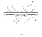
- FIG. 1 shows a cross-sectional view of a backlight module 100 in accordance with an embodiment of the present invention.
- the backlight module 100 is constructed on a double-sided MCPCB 110 comprising a top electrical conductive layer 111 , a top electrical insulating layer 112 , a core thermal conductive layer 113 made of thermal conducting material such as aluminum, a bottom insulating layer 114 and a bottom electrical conductive layer 115 .
- LED components which may be in different colors such as red LED 101 , green LED 102 and blue LED 103 , are mounted on the top electrical conductive layer 111 .
- Other electronics components such as LED driver ICs 116 , and passive components 117 are mounted on the bottom electrical conductive layer 115 .
- the electrical conductive layers 111 , 115 are patterned to form conductive pathways that connect electronics components 116 , 117 to form a driving circuit for driving LED components 101 , 102 , 103 .
- Ventilation windows 118 are created on the bottom layers 114 , 115 to expose the core layer 113 to ambient environment.
- the core layer 113 absorbs heat generated by LED components 101 , 102 , 103 and dissipates such heat energy to ambient environment through the ventilation windows 118 .
- FIG. 2 shows a planar view of the bottom side of the backlight module 100
- FIG. 3 shows a planar view of the top side.
- Connector sockets 201 , 301 are disposed on the peripheral of the module 100 to provide electrical connections to other backlight modules or a main circuit not shown in the figures.
- a heat dissipating structure which may be the back cover of the light box for housing the backlight modules, is further arranged to facilitate the heat dissipation.
- the back cover may be may be a planar structure with protruding portions that correspond to the ventilation windows on the backlight module circuit board. When the circuit board is installed into the light box, the protruding portions come into contact with the aluminum core layer. Accordingly, the aluminum core layer, together with the light box back cover, provides a more effective thermal dissipation channel, because the surface area of the light box back cover is greater than the ventilation window on the aluminum core layer
- FIG. 4 shows a cross-sectional view of a backlight module 400 in accordance with a further embodiment of the present invention.
- the arrangement is modified from the embodiment of FIG. 1 in that the back cover 401 of the light box under circuit board 110 where said back cover 401 has protruding portions 402 contacting the circuit board thermal conductive core layer 113 through the bottom layer ventilation window 118 .
- the back cover 401 structure may be made of materials such as aluminum, aluminum alloy, steel or copper.
- a thin thermal interface material 404 is added between the circuit board core layer 113 and light box back cover 401 .
- the heat dissipating structure which may be the back cover 401 of the light box, comprises windows 403 over the position of the electronic components as ventilation openings for the components to dissipate heat through convention.
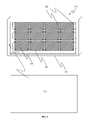
- a large backlight system can be composed by backlight modules described above.
- the modules are arranged laterally and fixed on the light box back cover.
- the backlight modules can be interconnected by flat cable connector.
- FIG. 5 shows a perspective view of a backlight system 500 assembled from backlight modules 100 of FIG. 1 .
- the backlight modules 100 are fixed on the back cover 401 of the light box 501 . Openings 502 are made on the back cover 401 for positioning cable connectors.
- the backlight module further includes an optical cover plate 503 which is disposed over the components of the light box.
- FIG. 6 shows a cross-sectional view of the connecting portions 600 between backlight modules 100 of FIG. 5 .
- the connector sockets 201 are arranged on the periphery of the backlight module circuit boards 110 a, 110 b. Openings 502 are made in the back cover 401 to accommodate the interconnections 601 between the circuit boards 110 a, 110 b, for example, a flat cable connector.
- the thermal management of the backlight system can be further enhanced by adding a heat sink to the light box back cover 401 .
- a thin thermal interface material 404 such as thermal grease can be added between the circuit board core layer 113 and light box back cover 401 at the contact region to reduce the thermal resistance across the two structures.
- FIG. 7 illustrates a method 700 of manufacturing the backlight module in accordance with an embodiment of the present invention.
- step 710 LED components of particular wavelengths, LED drivers, passive components and electrical connectors are provided according to the manufacturing specification.
- a MCPCB is fabricated with copper strips on the top and bottom surfaces to provide electrical connections for LED components and other electronic components. Thermal dissipation windows are further created on the bottom surface layer to expose the core thermal conductive layer.
- step 730 LED components are assembled on the top surface of the circuit board to form the illuminating side. For example, this may be done using soldering.
- the other electronic components such as LED drivers, passive components are assembled on the bottom surface. As such, a LED backlight module is formed.
- step 740 the LED backlight modules of step 730 are assembled laterally on the back cover of a light box, in such a way that the thermal contact protruding portions of the back cover contact the aluminum core layer exposed by ventilation windows on the bottom side of the backlight modules.
- the light box functions as a mechanical housing for the LED backlight system; on the other hand, the light box facilitates the heat dissipation for the system.
- a thin thermal interface material can be added between the backlight module and the light box at the contact region to reduce the thermal resistance across the two structures.
- step 750 the LED backlight modules mounted on the light box are connected together by flat cables or other connection methods.
- the flat cables also connect the modules to power supply unit and control unit of the backlight system.
- step 760 an optical reflector is assembled on top of the illuminating side of the LED backlight modules to diffuse the emitted light and provide a more uniform and even backlight illumination.
Landscapes
- Physics & Mathematics (AREA)
- Nonlinear Science (AREA)
- Engineering & Computer Science (AREA)
- Microelectronics & Electronic Packaging (AREA)
- Mathematical Physics (AREA)
- Chemical & Material Sciences (AREA)
- Crystallography & Structural Chemistry (AREA)
- General Physics & Mathematics (AREA)
- Optics & Photonics (AREA)
- Arrangement Of Elements, Cooling, Sealing, Or The Like Of Lighting Devices (AREA)
- Planar Illumination Modules (AREA)
- Liquid Crystal (AREA)
Abstract
Description
Claims (21)
Priority Applications (3)
| Application Number | Priority Date | Filing Date | Title |
|---|---|---|---|
| US11/640,587 US7607790B2 (en) | 2006-12-18 | 2006-12-18 | Backlighting apparatus and manufacturing process |
| CN2007800447174A CN101548226B (en) | 2006-12-18 | 2007-11-14 | Backlight device and its manufacturing process |
| PCT/CN2007/071060 WO2008074245A1 (en) | 2006-12-18 | 2007-11-14 | Blacklight apparatus and manufacturing method of the same |
Applications Claiming Priority (1)
| Application Number | Priority Date | Filing Date | Title |
|---|---|---|---|
| US11/640,587 US7607790B2 (en) | 2006-12-18 | 2006-12-18 | Backlighting apparatus and manufacturing process |
Publications (2)
| Publication Number | Publication Date |
|---|---|
| US20080144315A1 US20080144315A1 (en) | 2008-06-19 |
| US7607790B2 true US7607790B2 (en) | 2009-10-27 |
Family
ID=39526945
Family Applications (1)
| Application Number | Title | Priority Date | Filing Date |
|---|---|---|---|
| US11/640,587 Active US7607790B2 (en) | 2006-12-18 | 2006-12-18 | Backlighting apparatus and manufacturing process |
Country Status (3)
| Country | Link |
|---|---|
| US (1) | US7607790B2 (en) |
| CN (1) | CN101548226B (en) |
| WO (1) | WO2008074245A1 (en) |
Cited By (8)
| Publication number | Priority date | Publication date | Assignee | Title |
|---|---|---|---|---|
| US20100128193A1 (en) * | 2008-11-27 | 2010-05-27 | Jaeho Hwang | Liquid crystal display |
| US20100202130A1 (en) * | 2007-07-27 | 2010-08-12 | Akira Tomiyoshi | Illumination device and display device using the same |
| US20110013377A1 (en) * | 2007-09-11 | 2011-01-20 | Kim Deung Kwan | Light unit and display apparatus having the same |
| US20110037937A1 (en) * | 2008-05-27 | 2011-02-17 | Shenzhen New Supper-Bright Lcd Display Co.,Ltd. | Lcd apparatus with heat dissipation arrangements |
| US20120275153A1 (en) * | 2011-04-29 | 2012-11-01 | Zimmerman Joseph J | Flat panel light |
| US20140226341A1 (en) * | 2012-01-22 | 2014-08-14 | Ecolivegreen Corp. | Diffusion Globe LED Lighting Device |
| US20150148111A1 (en) * | 2012-08-06 | 2015-05-28 | Kmw Inc. | Closure apparatus of wireless communication device |
| US20180356686A1 (en) * | 2017-06-12 | 2018-12-13 | Innolux Corporation | Display device |
Families Citing this family (10)
| Publication number | Priority date | Publication date | Assignee | Title |
|---|---|---|---|---|
| TW200843548A (en) * | 2007-04-26 | 2008-11-01 | Chunghwa Picture Tubes Ltd | Light source module |
| JP4968014B2 (en) * | 2007-11-22 | 2012-07-04 | ソニー株式会社 | Backlight device and liquid crystal display device |
| JP5444343B2 (en) * | 2008-07-17 | 2014-03-19 | アイシス イノヴェイション リミテッド | Utility instrument |
| US20100046221A1 (en) * | 2008-08-19 | 2010-02-25 | Jason Loomis Posselt | LED Source Adapted for Light Bulbs and the Like |
| DE102009007498B4 (en) * | 2009-02-05 | 2022-12-08 | Osram Gmbh | Optoelectronic light module |
| GB2471497B (en) * | 2009-07-01 | 2014-08-20 | Tdk Lambda Uk Ltd | Heat sink |
| US8632207B2 (en) * | 2010-11-05 | 2014-01-21 | Lex Products Corporation | LED lighting apparatus and housing |
| TR201514689A2 (en) | 2015-11-20 | 2017-06-21 | Farba Otomotiv Aydinlatma Ve Plastik Fabrikalari Anonim Sirketi | The preferred light engine system in LED based lighting systems. |
| US20190250462A1 (en) * | 2018-02-12 | 2019-08-15 | Innolux Corporation | Display device |
| FR3078784B1 (en) * | 2018-03-09 | 2021-12-17 | Valeo Comfort & Driving Assistance | DISPLAY DEVICE |
Citations (6)
| Publication number | Priority date | Publication date | Assignee | Title |
|---|---|---|---|---|
| US4408255A (en) * | 1981-01-12 | 1983-10-04 | Harold Adkins | Absorptive electromagnetic shielding for high speed computer applications |
| US4480255A (en) * | 1982-12-06 | 1984-10-30 | Motorola Inc. | Method for achieving high isolation between antenna arrays |
| US5208732A (en) * | 1991-05-29 | 1993-05-04 | Texas Instruments, Incorporated | Memory card with flexible conductor between substrate and metal cover |
| US5836676A (en) * | 1996-05-07 | 1998-11-17 | Koha Co., Ltd. | Light emitting display apparatus |
| US20050180142A1 (en) | 2004-02-17 | 2005-08-18 | Yi-Shiuan Tsai | Backlight module and heat dissipation structure thereof |
| US20060002142A1 (en) | 2004-06-28 | 2006-01-05 | Lg.Philips Lcd Co., Ltd. | Backlight unit |
Family Cites Families (6)
| Publication number | Priority date | Publication date | Assignee | Title |
|---|---|---|---|---|
| CN2598077Y (en) * | 2003-01-23 | 2004-01-07 | 夏志清 | LED lattice module with convex transparent cover case |
| JP4701642B2 (en) * | 2004-07-05 | 2011-06-15 | 日本電気株式会社 | Display device |
| WO2006038778A1 (en) * | 2004-10-05 | 2006-04-13 | Samsung Electronics Co., Ltd. | Backlight unit |
| KR101157233B1 (en) * | 2004-10-30 | 2012-06-15 | 엘지디스플레이 주식회사 | Apparatus of light emitting diode backlight and liquid crystal display device using thereof |
| KR20060070159A (en) * | 2004-12-20 | 2006-06-23 | 삼성전자주식회사 | Backlight system and LCD using the same |
| TWI307799B (en) * | 2005-05-25 | 2009-03-21 | Coretronic Corp | Backlight module |
-
2006
- 2006-12-18 US US11/640,587 patent/US7607790B2/en active Active
-
2007
- 2007-11-14 CN CN2007800447174A patent/CN101548226B/en not_active Expired - Fee Related
- 2007-11-14 WO PCT/CN2007/071060 patent/WO2008074245A1/en not_active Ceased
Patent Citations (6)
| Publication number | Priority date | Publication date | Assignee | Title |
|---|---|---|---|---|
| US4408255A (en) * | 1981-01-12 | 1983-10-04 | Harold Adkins | Absorptive electromagnetic shielding for high speed computer applications |
| US4480255A (en) * | 1982-12-06 | 1984-10-30 | Motorola Inc. | Method for achieving high isolation between antenna arrays |
| US5208732A (en) * | 1991-05-29 | 1993-05-04 | Texas Instruments, Incorporated | Memory card with flexible conductor between substrate and metal cover |
| US5836676A (en) * | 1996-05-07 | 1998-11-17 | Koha Co., Ltd. | Light emitting display apparatus |
| US20050180142A1 (en) | 2004-02-17 | 2005-08-18 | Yi-Shiuan Tsai | Backlight module and heat dissipation structure thereof |
| US20060002142A1 (en) | 2004-06-28 | 2006-01-05 | Lg.Philips Lcd Co., Ltd. | Backlight unit |
Cited By (14)
| Publication number | Priority date | Publication date | Assignee | Title |
|---|---|---|---|---|
| US20100202130A1 (en) * | 2007-07-27 | 2010-08-12 | Akira Tomiyoshi | Illumination device and display device using the same |
| US20110013377A1 (en) * | 2007-09-11 | 2011-01-20 | Kim Deung Kwan | Light unit and display apparatus having the same |
| US8201959B2 (en) * | 2007-09-11 | 2012-06-19 | Lg Innotek Co., Ltd. | Light unit and display apparatus having the same |
| US8471997B2 (en) * | 2008-05-27 | 2013-06-25 | Shenzhen New Super-Bright Lcd Display Co., Ltd. | LCD apparatus with heat dissipation arrangements |
| US20110037937A1 (en) * | 2008-05-27 | 2011-02-17 | Shenzhen New Supper-Bright Lcd Display Co.,Ltd. | Lcd apparatus with heat dissipation arrangements |
| US8416360B2 (en) * | 2008-11-27 | 2013-04-09 | Lg Display Co., Ltd. | Liquid crystal display |
| US20100128193A1 (en) * | 2008-11-27 | 2010-05-27 | Jaeho Hwang | Liquid crystal display |
| US20120275153A1 (en) * | 2011-04-29 | 2012-11-01 | Zimmerman Joseph J | Flat panel light |
| US8919999B2 (en) * | 2011-04-29 | 2014-12-30 | Joy Mm Delaware, Inc. | Flat panel light with clear potting material |
| US20140226341A1 (en) * | 2012-01-22 | 2014-08-14 | Ecolivegreen Corp. | Diffusion Globe LED Lighting Device |
| US8985809B2 (en) * | 2012-01-22 | 2015-03-24 | Ecolivegreen Corp. | Diffusion globe LED lighting device |
| US20150148111A1 (en) * | 2012-08-06 | 2015-05-28 | Kmw Inc. | Closure apparatus of wireless communication device |
| US20180356686A1 (en) * | 2017-06-12 | 2018-12-13 | Innolux Corporation | Display device |
| US10527887B2 (en) * | 2017-06-12 | 2020-01-07 | Innolux Corporation | LED display device, has flexible circuit board comprising main and extension portions, where main portion is arranged on first surface and extension portion is arranged on second surface, and light-emitting units arranged on main portion |
Also Published As
| Publication number | Publication date |
|---|---|
| CN101548226B (en) | 2011-01-19 |
| WO2008074245A1 (en) | 2008-06-26 |
| CN101548226A (en) | 2009-09-30 |
| US20080144315A1 (en) | 2008-06-19 |
Similar Documents
| Publication | Publication Date | Title |
|---|---|---|
| WO2008074245A1 (en) | Blacklight apparatus and manufacturing method of the same | |
| JP5097461B2 (en) | Liquid crystal display and backlight module thereof | |
| KR101546741B1 (en) | Light emitting module and display apparatus having the same | |
| RU2518198C2 (en) | Light-emitting device | |
| US8550680B2 (en) | Lighting device | |
| TWI266432B (en) | Light emitting module | |
| US7505109B2 (en) | Heat dissipation structure of backlight module | |
| CN102484195B (en) | Light emitting device and light unit using the light emitting device | |
| JP2009003081A (en) | Display device and liquid crystal display device | |
| JP4969332B2 (en) | Substrate and lighting device | |
| US20080170177A1 (en) | Backlight Module and Liquid Crystal Display using the same | |
| US20070109788A1 (en) | Backlight module | |
| KR20080073085A (en) | Light emitting diode module and display device having same | |
| US8684550B2 (en) | Light source, light-emitting module having the same and backlight unit have the same | |
| US7374316B2 (en) | Backlight module | |
| US20080265781A1 (en) | Light source module | |
| JP2010225385A (en) | Backlight device | |
| JP2006208723A (en) | Liquid crystal display device | |
| CN100388092C (en) | Heat dissipation structure of backlight module | |
| JP2006066725A (en) | Semiconductor device having heat dissipation structure and method of assembling the same | |
| JP2007193946A (en) | Light emitting device | |
| JP2009152146A (en) | Surface light source device and display device | |
| JP4992636B2 (en) | Backlight device | |
| JP2010276628A (en) | Liquid crystal display | |
| JP2007109945A (en) | light source |
Legal Events
| Date | Code | Title | Description |
|---|---|---|---|
| AS | Assignment |
Owner name: HONG KONG APPLIED SCIENCE AND TECHNOLOGY RESEARCH Free format text: ASSIGNMENT OF ASSIGNORS INTEREST;ASSIGNORS:CHEN, SHOU LUNG;NG, KWAN WAH;LIU, YING;REEL/FRAME:019548/0012 Effective date: 20070226 |
|
| STCF | Information on status: patent grant |
Free format text: PATENTED CASE |
|
| FPAY | Fee payment |
Year of fee payment: 4 |
|
| FPAY | Fee payment |
Year of fee payment: 8 |
|
| MAFP | Maintenance fee payment |
Free format text: PAYMENT OF MAINTENANCE FEE, 12TH YEAR, LARGE ENTITY (ORIGINAL EVENT CODE: M1553); ENTITY STATUS OF PATENT OWNER: LARGE ENTITY Year of fee payment: 12 |