US7602832B2 - Surface emitting laser aligned with pump laser on single heat sink - Google Patents
Surface emitting laser aligned with pump laser on single heat sink Download PDFInfo
- Publication number
- US7602832B2 US7602832B2 US11/442,526 US44252606A US7602832B2 US 7602832 B2 US7602832 B2 US 7602832B2 US 44252606 A US44252606 A US 44252606A US 7602832 B2 US7602832 B2 US 7602832B2
- Authority
- US
- United States
- Prior art keywords
- laser
- pump
- laser chip
- heat sink
- light
- Prior art date
- Legal status (The legal status is an assumption and is not a legal conclusion. Google has not performed a legal analysis and makes no representation as to the accuracy of the status listed.)
- Active, expires
Links
Images


Classifications
-
- H—ELECTRICITY
- H01—ELECTRIC ELEMENTS
- H01S—DEVICES USING THE PROCESS OF LIGHT AMPLIFICATION BY STIMULATED EMISSION OF RADIATION [LASER] TO AMPLIFY OR GENERATE LIGHT; DEVICES USING STIMULATED EMISSION OF ELECTROMAGNETIC RADIATION IN WAVE RANGES OTHER THAN OPTICAL
- H01S5/00—Semiconductor lasers
- H01S5/10—Construction or shape of the optical resonator, e.g. extended or external cavity, coupled cavities, bent-guide, varying width, thickness or composition of the active region
- H01S5/18—Surface-emitting [SE] lasers, e.g. having both horizontal and vertical cavities
- H01S5/183—Surface-emitting [SE] lasers, e.g. having both horizontal and vertical cavities having only vertical cavities, e.g. vertical cavity surface-emitting lasers [VCSEL]
- H01S5/18386—Details of the emission surface for influencing the near- or far-field, e.g. a grating on the surface
- H01S5/18388—Lenses
-
- H—ELECTRICITY
- H01—ELECTRIC ELEMENTS
- H01S—DEVICES USING THE PROCESS OF LIGHT AMPLIFICATION BY STIMULATED EMISSION OF RADIATION [LASER] TO AMPLIFY OR GENERATE LIGHT; DEVICES USING STIMULATED EMISSION OF ELECTROMAGNETIC RADIATION IN WAVE RANGES OTHER THAN OPTICAL
- H01S5/00—Semiconductor lasers
- H01S5/005—Optical components external to the laser cavity, specially adapted therefor, e.g. for homogenisation or merging of the beams or for manipulating laser pulses, e.g. pulse shaping
- H01S5/0071—Optical components external to the laser cavity, specially adapted therefor, e.g. for homogenisation or merging of the beams or for manipulating laser pulses, e.g. pulse shaping for beam steering, e.g. using a mirror outside the cavity to change the beam direction
-
- H—ELECTRICITY
- H01—ELECTRIC ELEMENTS
- H01S—DEVICES USING THE PROCESS OF LIGHT AMPLIFICATION BY STIMULATED EMISSION OF RADIATION [LASER] TO AMPLIFY OR GENERATE LIGHT; DEVICES USING STIMULATED EMISSION OF ELECTROMAGNETIC RADIATION IN WAVE RANGES OTHER THAN OPTICAL
- H01S5/00—Semiconductor lasers
- H01S5/02—Structural details or components not essential to laser action
- H01S5/022—Mountings; Housings
- H01S5/0225—Out-coupling of light
- H01S5/02255—Out-coupling of light using beam deflecting elements
-
- H—ELECTRICITY
- H01—ELECTRIC ELEMENTS
- H01S—DEVICES USING THE PROCESS OF LIGHT AMPLIFICATION BY STIMULATED EMISSION OF RADIATION [LASER] TO AMPLIFY OR GENERATE LIGHT; DEVICES USING STIMULATED EMISSION OF ELECTROMAGNETIC RADIATION IN WAVE RANGES OTHER THAN OPTICAL
- H01S5/00—Semiconductor lasers
- H01S5/02—Structural details or components not essential to laser action
- H01S5/022—Mountings; Housings
- H01S5/023—Mount members, e.g. sub-mount members
- H01S5/02325—Mechanically integrated components on mount members or optical micro-benches
-
- H—ELECTRICITY
- H01—ELECTRIC ELEMENTS
- H01S—DEVICES USING THE PROCESS OF LIGHT AMPLIFICATION BY STIMULATED EMISSION OF RADIATION [LASER] TO AMPLIFY OR GENERATE LIGHT; DEVICES USING STIMULATED EMISSION OF ELECTROMAGNETIC RADIATION IN WAVE RANGES OTHER THAN OPTICAL
- H01S5/00—Semiconductor lasers
- H01S5/02—Structural details or components not essential to laser action
- H01S5/024—Arrangements for thermal management
- H01S5/02469—Passive cooling, e.g. where heat is removed by the housing as a whole or by a heat pipe without any active cooling element like a TEC
-
- H—ELECTRICITY
- H01—ELECTRIC ELEMENTS
- H01S—DEVICES USING THE PROCESS OF LIGHT AMPLIFICATION BY STIMULATED EMISSION OF RADIATION [LASER] TO AMPLIFY OR GENERATE LIGHT; DEVICES USING STIMULATED EMISSION OF ELECTROMAGNETIC RADIATION IN WAVE RANGES OTHER THAN OPTICAL
- H01S5/00—Semiconductor lasers
- H01S5/04—Processes or apparatus for excitation, e.g. pumping, e.g. by electron beams
- H01S5/041—Optical pumping
-
- H—ELECTRICITY
- H01—ELECTRIC ELEMENTS
- H01S—DEVICES USING THE PROCESS OF LIGHT AMPLIFICATION BY STIMULATED EMISSION OF RADIATION [LASER] TO AMPLIFY OR GENERATE LIGHT; DEVICES USING STIMULATED EMISSION OF ELECTROMAGNETIC RADIATION IN WAVE RANGES OTHER THAN OPTICAL
- H01S5/00—Semiconductor lasers
- H01S5/10—Construction or shape of the optical resonator, e.g. extended or external cavity, coupled cavities, bent-guide, varying width, thickness or composition of the active region
- H01S5/14—External cavity lasers
- H01S5/141—External cavity lasers using a wavelength selective device, e.g. a grating or etalon
-
- H—ELECTRICITY
- H01—ELECTRIC ELEMENTS
- H01S—DEVICES USING THE PROCESS OF LIGHT AMPLIFICATION BY STIMULATED EMISSION OF RADIATION [LASER] TO AMPLIFY OR GENERATE LIGHT; DEVICES USING STIMULATED EMISSION OF ELECTROMAGNETIC RADIATION IN WAVE RANGES OTHER THAN OPTICAL
- H01S3/00—Lasers, i.e. devices using stimulated emission of electromagnetic radiation in the infrared, visible or ultraviolet wave range
- H01S3/10—Controlling the intensity, frequency, phase, polarisation or direction of the emitted radiation, e.g. switching, gating, modulating or demodulating
- H01S3/106—Controlling the intensity, frequency, phase, polarisation or direction of the emitted radiation, e.g. switching, gating, modulating or demodulating by controlling devices placed within the cavity
- H01S3/108—Controlling the intensity, frequency, phase, polarisation or direction of the emitted radiation, e.g. switching, gating, modulating or demodulating by controlling devices placed within the cavity using non-linear optical devices, e.g. exhibiting Brillouin or Raman scattering
- H01S3/109—Frequency multiplication, e.g. harmonic generation
Definitions
- the present disclosure relates to an optical pumping type vertical external cavity surface emitting laser (VECSEL), and more particularly, to a VECSEL aligned with a pump laser on a single heat sink in one piece.
- VECSEL vertical external cavity surface emitting laser
- an edge emitting laser emits a laser beam in a horizontal direction to a substrate
- a surface emitting laser or vertical cavity surface emitting laser (VCSEL) emits a laser beam in a vertical direction to a substrate. Since the VCSEL oscillates in single longitudinal mode of a very narrow spectrum and emits a beam having a small radiation angle, it has advantages wherein coupling efficiency is high and integration with other devices can be readily achieved.
- a conventional VCSEL makes single transverse mode oscillation difficult in comparison with an edge emitting laser. Further, since single transverse mode operation of the conventional VCSEL requires a small oscillation region, the output is low.
- VECSEL vertical external cavity surface emitting laser
- FIG. 1 is a schematic sectional view of an optical pumped VECSEL according to the related art.
- a conventional optical pumping type VECSEL includes a laser chip 10 for laser oscillation, a heat sink 20 on which the laser chip 10 is attached through a bonding layer 21 , and an external mirror 22 spaced a predetermined distance apart from the laser chip 10 .
- the VECSEL further includes two pump lasers 25 and 26 arranged at both sides at angles to provide pump laser beams to the laser chip 10 .
- the laser chip 10 includes a distributed Bragg reflector (DBR) layer 16 , an active layer 18 , and an anti-reflection layer 12 that are sequentially stacked on a substrate 14 .
- DBR distributed Bragg reflector
- the active layer 18 has a multi quantum well structure with a resonant periodic gain (RPG) structure and emits light at a predetermined wavelength when activated by a pump laser beam.
- the heat sink 20 cools the laser chip 10 by dissipating heat generated from the laser chip 10 .
- the pump lasers 25 and 26 emit light at a wavelength shorter than that of the light emitted from the laser chip 10 to the laser chip 10 through lenses 27 and 28 in order to activate the active layer 18 of the laser chip 10 .
- the active layer 18 of the laser chip 10 when light emitted from the pump lasers 25 and 26 at a relatively short wavelength is incident on the laser chip 10 through the lenses 27 and 28 , the active layer 18 of the laser chip 10 is activated to generate light at a specific wavelength.
- the light generated from the active layer 18 is repeatedly reflected between the DBR layer 16 of the laser chip 10 and the external mirror 22 through the active layer 18 . Therefore, a resonance cavity of the VECSEL is defined between the DBR layer 16 of the laser chip 10 and a concave surface of the external mirror 22 .
- the light is amplified in the laser chip 10 , and then a portion of the light is outputted to the outside as a laser beam through the external mirror 22 and the other portion of the light is reflected again to the laser chip 10 as pump light.
- the conventional VECSEL with the aforementioned structure requires additional heat sinks to cool the pump lasers 25 and 26 besides the heat sink 20 cooling the laser chip 10 . Therefore, the laser chip 10 and the pump lasers 25 and 26 cannot be combined into a single module, and this leads to a limitation in reducing the overall size of the VECSEL. Further, an additional process is required to align the laser chip 10 and the pump lasers 25 and 26 . Furthermore, in practice, it is difficult to precisely align the laser chip 10 and the pump lasers 25 and 26 . As a result, the overall manufacturing process of the VECSEL is complicated and is lengthened. Therefore, it is difficult to mass produce the VECSEL, and the manufacturing cost of the VECSEL increases.
- the present invention may provide a smaller VECSEL in which a pump laser and a laser chip are integrally mounted on the single heat sink such that an additional process for precisely aligning the pump laser is not required and the VECSEL can be mass produced with less cost.
- a surface emitting laser including: a heat sink; a laser chip having a gain structure to emit light at a predetermined wavelength and disposed on a center portion of a top surface of the heat sink; an external mirror spaced apart from the laser chip at a predetermined distance to transmit a portion of the light emitted from the laser chip to outside the surface emitting laser and to reflect the remaining portion of the light to the laser chip; a pump laser disposed on one side of a top surface of the heat sink to emit pump light in a horizontal direction for activating the laser chip; and a reflection mirror disposed on the other side of the top surface of the heat sink opposite to the pump laser to reflect the pump light emitted from the pump laser to the laser chip.
- the reflection mirror may be a concave spherical mirror.
- the distance between the laser chip and the spherical mirror may be less than half the radius of curvature of the spherical mirror.
- the radius of curvature of the spherical mirror may be in the range of approximately 10 mm to 100 mm.
- the surface emitting laser may further include a collimating lens between the pump laser and the reflection mirror to convert the pump light emitted from the pump laser into parallel light.
- the collimating lens may be attached to a light output surface of the pump laser.
- the surface emitting laser may further include an SHG crystal between the laser chip and the external mirror to double the frequency of the light emitted from the laser chip.
- the temperature of the pump laser or the laser chip may be controlled by additionally disposing a TEC between the pump laser and the heat sink or between the laser chip and the heat sink.
- a surface emitting laser including: a heat sink defining an opening through a center portion in a vertical direction; a laser chip having a gain structure to emit light at a predetermined wavelength and disposed in the opening of the heat sink; an external mirror spaced apart from a top surface of the heat sink to transmit a portion of the light emitted from the laser chip to outside the surface emitting laser and to reflect the remaining portion of the light to the laser chip; a pump laser disposed on one side of a bottom surface of the heat sink to emit pump light in a horizontal direction for activating of the laser chip; and a reflection mirror disposed on the other side of the bottom surface of the heat sink opposite to the pump laser to reflect the pump light emitted from the pump laser to the laser chip.
- FIG. 1 is a sectional view schematically showing a conventional optical pumping type VECSEL
- FIG. 2 is a sectional view schematically showing an optical pumping type VECSEL according to a first embodiment of the present invention
- FIG. 3 is a sectional view schematically showing an optical pumping type VECSEL according to a second embodiment of the present invention
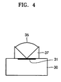
- FIG. 4 exemplarily shows a shape of a spherical mirror according to the present invention.
- FIGS. 5A and 5B are profile graphs of a pump laser beam emitted from a pump laser toward a laser chip according to the present invention.
- FIG. 2 is a sectional view schematically showing an optical pumping type VECSEL according to a first embodiment of the present invention.
- the surface emitting laser includes a heat sink 30 , a laser chip 31 disposed on a top of the heat sink 30 at a center portion, and a pump laser 33 disposed on a top of the heat sink 30 at a side portion to activate the laser chip 31 .
- the surface emitting laser includes a reflection mirror 35 disposed on a top of the heat sink 30 at the other side portion to reflect pump light emitted from the pump laser 33 to the laser chip 31 . Therefore, the pump laser 33 and the reflection mirror 35 confront (oppose) each other on the heat sink 30 .
- the surface emitting laser includes an external mirror 36 spaced apart from the laser chip 31 at a predetermined distance to output a laser beam by transmitting a portion of light emitted from the laser chip 31 and to reflect the other (remaining) portion of the light back to the laser chip 31 .
- the surface emitting laser can further include a second harmonic generation (SHG) crystal 38 between the laser chip 31 and the external mirror 36 to double the frequency of the light emitted from the laser chip 31 (i.e., to reduce the wavelength of the light by half) so as to output a visible laser beam.
- SHG second harmonic generation
- the surface emitting laser with the aforementioned structure operates as follows.
- the pump laser 33 confronting the reflection mirror 35 emits pump laser light at a predetermined wavelength in a horizontal direction.
- the wavelength of the pump light emitted from the pump laser 33 is shorter than that of the light to be emitted from the laser chip 31 .
- a pump laser emitting light at a wavelength of about 808 nm can be used.
- a collimating lens 34 may be disposed between the pump laser 33 and the reflection mirror 35 to convert the pump laser light emitted from the pump laser 33 into parallel light.
- the collimating lens 34 may be attached to a light exit surface of the pump laser 33 .
- the parallel light from the collimating lens 34 is reflected by the reflection mirror 35 confronting the pump laser 33 so as to be focused on the laser chip 31 .
- the reflection mirror 35 may be a spherical mirror with a concave reflecting surface.
- the laser chip 31 may be located within a focal length of the spherical reflection mirror 35 . That is, it is preferable that the horizontal distance between the laser chip 31 and the reflection mirror 35 is less than half the radius of curvature of the reflection mirror 35 .
- the radius of curvature of the reflection mirror 35 is determined depending on the size and output power of the surface emitting laser to be manufactured, and it is generally appropriate that the radius of curvature of the reflection mirror 35 is in the range of approximately 10 mm to 100 mm. Further, the reflecting surface of the reflection mirror 35 may be coated with metal or dielectric material with a high reflectance to reflect most of the pump light emitted from the pump laser 33 to the laser chip 31 .
- a spherical mirror can be divided into several parts for being used as the reflection mirror 35 , though the entire spherical mirror can be used as the reflection mirror 35 .
- a quarter of a spherical mirror can be fixed to the heat sink 30 using a support 37 to use the quarter for the reflection mirror 35 .
- a mirror piece obtained by dividing a spherical mirror into more pieces can be used. In this case, a number of surface emitting lasers can be manufactured by dividing a single spherical mirror.
- the structure of the laser chip 31 has the same structure as the laser chip used in the conventional VECSEL. That is, as described above, the laser chip 31 includes a DBR layer (not shown) and the active layer (not shown) that are sequentially formed on a substrate (not shown).
- the active layer for example, has a gain structure of a multi quantum well structure such as a resonant periodic gain (RPG) structure. The light generated in this manner is amplified while it is repeatedly reflected between the DBR layer in the laser chip 31 and the external mirror 36 .
- RPG resonant periodic gain
- a portion of the amplified light is outputted to the outside through the external mirror 36 as a laser beam, and the remaining portion is reflected again to the laser chip 31 .
- the SHG crystal 38 is placed between the laser chip 31 and the external mirror 36 , the wavelength of the laser beam outputted through the external mirror 36 is half the wavelength of the light emitted from laser chip 31 . Therefore, if the laser chip 31 emits infrared light, a visible laser beam can be outputted through the external mirror 36 .
- the pump laser 33 and the laser chip 31 generate much heat.
- the heat generated from the pump laser 33 and the laser chip 31 is dissipated to the outside only through the single heat sink 30 .
- a thermo electric cooler (TEC) can be used to increase cooling efficiency for the pump laser 33 and the laser chip 31 . That is, as shown in FIG. 2 , a TEC 32 can be additionally installed between the pump laser 33 and the heat sink 30 . Though the TEC is installed under the pump laser 33 in FIG. 2 , another TEC can be installed under the laser chip 31 .
- a TEC is a device that keeps a constant temperature difference between its both sides when a current is applied thereto.
- the temperature of the pump laser 33 can be controlled at a constant value by keeping the heat sink 30 at a constant temperature through, for example, water cooling.
- both the pump laser and the laser chip are mounted on the single heat sink. Therefore, unlike the related art, the pump laser and the laser chip do not require separate heat sinks, respectively, thereby reducing the number of heat sinks required and the overall size of the surface emitting laser. Further, since the pump laser and the laser chip are mounted on the single heat sink at the same time, the pump laser and the laser chip can be simply and easily aligned without requiring an additional process for precisely aligning the pump laser and the laser chip. As a result, the manufacturing process and time can be reduced, thereby allowing mass production with less cost.
- the concave spherical mirror is used to focus the pump light on the laser chip instead of using a lens array, optical loss and aberration occurring when light passes a plurality of lenses can be minimized, and also beam blur of the pump light can be minimized.
- FIGS. 5A and 5B are profile graphs of a pump laser beam emitted from the pump laser 33 to the laser chip 31 , FIG. 5A being a section taken along x-axis, FIG. 5B being a section taken along y-axis.
- a full width at half maximum of a pump laser beam reflected by the concave, spherical reflection mirror 35 is approximately 111.4 ⁇ m with respect to x-axis and approximately 136.6 ⁇ m with respect to y-axis. As shown in FIG.
- the pump laser beam on the laser chip 31 has an elliptical shape with different beam diameters along x-axis and y-axis.
- the optical distribution along each axis is approximately symmetrical.
- general VECSELs require a pump laser beam with a diameter of approximately 50 to 500 ⁇ m, the pump laser beam sufficiently meets the diameter constraint of the pump laser beam.
- FIG. 3 is a sectional view schematically showing a VECSEL according to a second embodiment of the present invention.
- the pumping structure of the VECSEL shown in FIG. 2 is a front-end pumping structure.
- a back-end pumping structure can be employed for more efficient laser oscillation.
- the surface emitting laser of the second embodiment of the present invention includes a heat sink 40 , and a pump laser 43 and a reflection mirror 45 that confront each other on the heat sink 40 .
- the heat sink 40 defines an opening 49 through a center portion in a vertical direction, and a laser chip 41 is disposed in the opening 49 . Though, in FIG.
- the laser chip 41 is disposed in the opening 49 at a bottom portion of the heat sink 40 , the position of the laser chip 41 in the opening 49 can vary depending on the design.
- a TEC 42 can be disposed between the pump laser 43 and the heat sink 40 .
- another TEC can be disposed between the laser chip 41 and the heat sink 40 .
- the surface emitting laser of the embodiments of the present invention is designed such that both the pump laser and the laser chip are mounted on the single heat sink. Therefore, unlike the conventional laser device that requires the heat sink for each of the pump laser and the laser chip, the number of heat sinks required can be reduced and the overall size of the surface emitting laser can be reduced. Further, since the pump laser and the laser chip are mounted on the single heat sink at the same time, the pump laser and the laser chip can be simply and easily aligned without requiring an additional process for precisely aligning the pump laser and the laser chip. As a result, the manufacturing process can be simplified, thereby making possible mass production with reduced cost.
- the concave spherical mirror is used to focus the pump light on the laser chip instead of using a lens array, optical loss and aberration occurring when light passes a plurality of lenses can be minimized, and also beam blur of the pump light can be minimized.
Landscapes
- Physics & Mathematics (AREA)
- Condensed Matter Physics & Semiconductors (AREA)
- General Physics & Mathematics (AREA)
- Electromagnetism (AREA)
- Optics & Photonics (AREA)
- Semiconductor Lasers (AREA)
- Optical Modulation, Optical Deflection, Nonlinear Optics, Optical Demodulation, Optical Logic Elements (AREA)
- Lasers (AREA)
Abstract
Description
Claims (15)
Applications Claiming Priority (2)
| Application Number | Priority Date | Filing Date | Title |
|---|---|---|---|
| KR1020050047192A KR100718128B1 (en) | 2005-06-02 | 2005-06-02 | Surface-emitting laser combined with pump laser on a single heat sink |
| KR10-2005-0047192 | 2005-06-02 |
Publications (2)
| Publication Number | Publication Date |
|---|---|
| US20060274807A1 US20060274807A1 (en) | 2006-12-07 |
| US7602832B2 true US7602832B2 (en) | 2009-10-13 |
Family
ID=37494054
Family Applications (1)
| Application Number | Title | Priority Date | Filing Date |
|---|---|---|---|
| US11/442,526 Active 2026-06-25 US7602832B2 (en) | 2005-06-02 | 2006-05-30 | Surface emitting laser aligned with pump laser on single heat sink |
Country Status (3)
| Country | Link |
|---|---|
| US (1) | US7602832B2 (en) |
| JP (1) | JP2006339638A (en) |
| KR (1) | KR100718128B1 (en) |
Families Citing this family (9)
| Publication number | Priority date | Publication date | Assignee | Title |
|---|---|---|---|---|
| DE102006017294A1 (en) * | 2005-12-30 | 2007-07-05 | Osram Opto Semiconductors Gmbh | Optically pumpable semiconductor device for use in resonator, has surface-emitting semiconductor body which is provided with radiation penetration surface that faces away from mounting plane of semiconductor body |
| EP2320215B1 (en) * | 2009-11-06 | 2013-05-01 | Axetris AG | Semiconductor laser system for gas detection with integrated and thermally controlled beam shaping element |
| US8432609B2 (en) * | 2010-01-20 | 2013-04-30 | Northrop Grumman Systems Corporation | Photo-pumped semiconductor optical amplifier |
| RU2654303C2 (en) * | 2012-12-11 | 2018-05-17 | Конинклейке Филипс Н.В. | Optically pumped solid state laser device with self aligning pump optics and enhanced gain |
| CN105706315B (en) * | 2013-10-30 | 2019-08-06 | 皇家飞利浦有限公司 | Laser equipment including optically pumped extended cavity lasers |
| KR101643925B1 (en) * | 2014-07-23 | 2016-08-11 | 울산과학기술원 | A laser heat treatment method of steel sheets |
| EP3219360B1 (en) | 2014-11-10 | 2020-05-06 | Sanhe Laserconn Tech Co., Ltd. | High power vcsel laser treatment device with skin cooling function and packaging structure thereof |
| CN111162444B (en) * | 2019-12-31 | 2021-08-17 | 芯思杰技术(深圳)股份有限公司 | Chip packaging method |
| EP4199276A1 (en) * | 2021-12-14 | 2023-06-21 | Twenty-One Semiconductors GmbH | Optically pumped semiconductor laser arrangement |
Citations (4)
| Publication number | Priority date | Publication date | Assignee | Title |
|---|---|---|---|---|
| US6097742A (en) * | 1999-03-05 | 2000-08-01 | Coherent, Inc. | High-power external-cavity optically-pumped semiconductor lasers |
| US6243407B1 (en) * | 1997-03-21 | 2001-06-05 | Novalux, Inc. | High power laser devices |
| US6327291B1 (en) * | 1995-11-22 | 2001-12-04 | Iridex Corporation | Fiber stub end-pumped laser |
| US20050036528A1 (en) * | 2001-09-28 | 2005-02-17 | Wolfgang Schmid | Optically pumped, vertically emitting semiconductor laser |
Family Cites Families (4)
| Publication number | Priority date | Publication date | Assignee | Title |
|---|---|---|---|---|
| JPH08204256A (en) * | 1994-09-20 | 1996-08-09 | Fuji Photo Film Co Ltd | Laser diode pumping solid-state laser |
| JP3378103B2 (en) * | 1994-12-28 | 2003-02-17 | 富士写真フイルム株式会社 | Laser diode pumped solid state laser |
| US6327293B1 (en) | 1998-08-12 | 2001-12-04 | Coherent, Inc. | Optically-pumped external-mirror vertical-cavity semiconductor-laser |
| JP2001223429A (en) | 2000-02-09 | 2001-08-17 | Fuji Photo Film Co Ltd | Semiconductor laser device |
-
2005
- 2005-06-02 KR KR1020050047192A patent/KR100718128B1/en not_active Expired - Fee Related
-
2006
- 2006-05-23 JP JP2006143270A patent/JP2006339638A/en active Pending
- 2006-05-30 US US11/442,526 patent/US7602832B2/en active Active
Patent Citations (4)
| Publication number | Priority date | Publication date | Assignee | Title |
|---|---|---|---|---|
| US6327291B1 (en) * | 1995-11-22 | 2001-12-04 | Iridex Corporation | Fiber stub end-pumped laser |
| US6243407B1 (en) * | 1997-03-21 | 2001-06-05 | Novalux, Inc. | High power laser devices |
| US6097742A (en) * | 1999-03-05 | 2000-08-01 | Coherent, Inc. | High-power external-cavity optically-pumped semiconductor lasers |
| US20050036528A1 (en) * | 2001-09-28 | 2005-02-17 | Wolfgang Schmid | Optically pumped, vertically emitting semiconductor laser |
Also Published As
| Publication number | Publication date |
|---|---|
| KR20060125250A (en) | 2006-12-06 |
| US20060274807A1 (en) | 2006-12-07 |
| KR100718128B1 (en) | 2007-05-14 |
| JP2006339638A (en) | 2006-12-14 |
Similar Documents
| Publication | Publication Date | Title |
|---|---|---|
| US8576885B2 (en) | Optical pump for high power laser | |
| US20210351569A1 (en) | Semiconductor laser | |
| US20070268941A1 (en) | Vertical external cavity surface emitting laser and method thereof | |
| JP5322374B2 (en) | External cavity surface emitting laser | |
| US7602832B2 (en) | Surface emitting laser aligned with pump laser on single heat sink | |
| US7397829B2 (en) | Vertical external cavity surface emitting laser | |
| US7548569B2 (en) | High-power optically end-pumped external-cavity semiconductor laser | |
| CN117977383A (en) | A compact all-semiconductor laser based on VCSELs pumping VECSEL gain chip | |
| US7406108B2 (en) | Vertical external cavity surface emitting laser (VECSEL) | |
| US20060280220A1 (en) | Optically-pumped vertical external cavity surface emitting laser | |
| KR101100434B1 (en) | External resonator type surface emitting laser with rear light pumping | |
| WO2015055589A1 (en) | Hermetically sealed container for laser device | |
| US20070133640A1 (en) | Vertical external cavity surface emitting laser with pump beam reflector | |
| US7486714B2 (en) | Pump laser integrated vertical external cavity surface emitting laser | |
| KR100714609B1 (en) | Visible light laser device | |
| KR101334175B1 (en) | Vertical external cavity surface emitting laser having lens duct | |
| CN117878716A (en) | Laser device for optically pumped VCSEL external cavity spectrum synthesis | |
| KR20070074750A (en) | External resonator type surface emitting laser | |
| JP2005019804A (en) | Semiconductor laser device | |
| KR20070058246A (en) | External resonator type surface emitting laser with rear light pumping | |
| JP2007266532A (en) | Semiconductor laser device |
Legal Events
| Date | Code | Title | Description |
|---|---|---|---|
| AS | Assignment |
Owner name: SAMSUNG ELECTRONICS CO., LTD., KOREA, REPUBLIC OF Free format text: ASSIGNMENT OF ASSIGNORS INTEREST;ASSIGNOR:SAMSUNG ELECTRONICS CO., LTD.;REEL/FRAME:017943/0621 Effective date: 20060525 |
|
| AS | Assignment |
Owner name: SAMSUNG ELECTRONICS CO., LTD., KOREA, REPUBLIC OF Free format text: CORRECT NAME OF CONVEYING PARTIES AND EXECUTION AND DATE AND NAME OF RECEIVING PARTY RECORDED AT R/F 017943/0621;ASSIGNORS:CHO, SOO-HAENG;LIM, SEONG-JIN;REEL/FRAME:018322/0923 Effective date: 20060525 |
|
| STCF | Information on status: patent grant |
Free format text: PATENTED CASE |
|
| FEPP | Fee payment procedure |
Free format text: PAYOR NUMBER ASSIGNED (ORIGINAL EVENT CODE: ASPN); ENTITY STATUS OF PATENT OWNER: LARGE ENTITY |
|
| FEPP | Fee payment procedure |
Free format text: PAYER NUMBER DE-ASSIGNED (ORIGINAL EVENT CODE: RMPN); ENTITY STATUS OF PATENT OWNER: LARGE ENTITY Free format text: PAYOR NUMBER ASSIGNED (ORIGINAL EVENT CODE: ASPN); ENTITY STATUS OF PATENT OWNER: LARGE ENTITY |
|
| FPAY | Fee payment |
Year of fee payment: 4 |
|
| FPAY | Fee payment |
Year of fee payment: 8 |
|
| MAFP | Maintenance fee payment |
Free format text: PAYMENT OF MAINTENANCE FEE, 12TH YEAR, LARGE ENTITY (ORIGINAL EVENT CODE: M1553); ENTITY STATUS OF PATENT OWNER: LARGE ENTITY Year of fee payment: 12 |