US7585775B1 - System and method for faceting a masking layer in a plasma etch to slope a feature edge - Google Patents

System and method for faceting a masking layer in a plasma etch to slope a feature edge Download PDF

Info

Publication number
US7585775B1
US7585775B1 US11/285,702 US28570205A US7585775B1 US 7585775 B1 US7585775 B1 US 7585775B1 US 28570205 A US28570205 A US 28570205A US 7585775 B1 US7585775 B1 US 7585775B1
Authority
US
United States
Prior art keywords
layer
plasma etch
semiconductor device
etch process
sloped surface
Prior art date
Legal status (The legal status is an assumption and is not a legal conclusion. Google has not performed a legal analysis and makes no representation as to the accuracy of the status listed.)
Active, expires
Application number
US11/285,702
Inventor
Thomas Bold
Victor Torres
Rodney Hill
Current Assignee (The listed assignees may be inaccurate. Google has not performed a legal analysis and makes no representation or warranty as to the accuracy of the list.)
National Semiconductor Corp
Original Assignee
National Semiconductor Corp
Priority date (The priority date is an assumption and is not a legal conclusion. Google has not performed a legal analysis and makes no representation as to the accuracy of the date listed.)
Filing date
Publication date
Application filed by National Semiconductor Corp filed Critical National Semiconductor Corp
Priority to US11/285,702 priority Critical patent/US7585775B1/en
Assigned to NATIONAL SEMICONDUCTOR CORPORATION reassignment NATIONAL SEMICONDUCTOR CORPORATION ASSIGNMENT OF ASSIGNORS INTEREST (SEE DOCUMENT FOR DETAILS). Assignors: HILL, RODNEY, TORRES, VICTOR, BOLD, THOMAS
Application granted granted Critical
Publication of US7585775B1 publication Critical patent/US7585775B1/en
Active legal-status Critical Current
Adjusted expiration legal-status Critical

Links

Images

Classifications

    • HELECTRICITY
    • H01ELECTRIC ELEMENTS
    • H01LSEMICONDUCTOR DEVICES NOT COVERED BY CLASS H10
    • H01L21/00Processes or apparatus adapted for the manufacture or treatment of semiconductor or solid state devices or of parts thereof
    • H01L21/02Manufacture or treatment of semiconductor devices or of parts thereof
    • H01L21/04Manufacture or treatment of semiconductor devices or of parts thereof the devices having at least one potential-jump barrier or surface barrier, e.g. PN junction, depletion layer or carrier concentration layer
    • H01L21/18Manufacture or treatment of semiconductor devices or of parts thereof the devices having at least one potential-jump barrier or surface barrier, e.g. PN junction, depletion layer or carrier concentration layer the devices having semiconductor bodies comprising elements of Group IV of the Periodic System or AIIIBV compounds with or without impurities, e.g. doping materials
    • H01L21/30Treatment of semiconductor bodies using processes or apparatus not provided for in groups H01L21/20 - H01L21/26
    • H01L21/31Treatment of semiconductor bodies using processes or apparatus not provided for in groups H01L21/20 - H01L21/26 to form insulating layers thereon, e.g. for masking or by using photolithographic techniques; After treatment of these layers; Selection of materials for these layers
    • H01L21/3205Deposition of non-insulating-, e.g. conductive- or resistive-, layers on insulating layers; After-treatment of these layers
    • H01L21/321After treatment
    • H01L21/3213Physical or chemical etching of the layers, e.g. to produce a patterned layer from a pre-deposited extensive layer
    • H01L21/32133Physical or chemical etching of the layers, e.g. to produce a patterned layer from a pre-deposited extensive layer by chemical means only
    • H01L21/32135Physical or chemical etching of the layers, e.g. to produce a patterned layer from a pre-deposited extensive layer by chemical means only by vapour etching only
    • H01L21/32136Physical or chemical etching of the layers, e.g. to produce a patterned layer from a pre-deposited extensive layer by chemical means only by vapour etching only using plasmas

Abstract

A method is disclosed for applying a plasma etch process to facet a masking layer in a semiconductor device by creating sloped surfaces in the masking layer. The masking layer is plasma etched with a plasma that has a high sputter etch component. The plasma etch process removes material from vertical edges of the masking layer to form a sloped surface at each vertical edge of the masking layer. A layer of conductive material is then applied to the masking layer. When the layer of conductive material is subsequently removed by an overetch process the sloped profile of the masking layer facilitates the removal of stringers of conductive material without using an excessively lengthy overetch.

Description

TECHNICAL FIELD OF THE INVENTION
The present invention is generally directed to manufacturing technology for semiconductor devices and, in particular, to a system and method for faceting a masking layer in a plasma etch to slope a feature edge.
BACKGROUND OF THE INVENTION
In the manufacture of a semiconductor device a layer of conductive material (e.g., metal) may be deposited over an underlying structure. When portions of the layer of conductive material are later etched away there are usually some residual stringers of conductive material that are not removed from the features of the underlying structure. The stringers of conductive material usually remain at the corners of vertical feature edges. An excessive overetch process is usually required in order to remove the stringers of conductive material from the corners of the vertical feature edges.
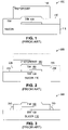
For example, consider the prior art semiconductor device 100 shown in FIG. 1. The semiconductor device 100 comprises a silicon or silicon dioxide substrate 110, a thin film resistor (TFR) 120, a titanium tungsten (TiW) protective layer 130, and a patterned photoresist layer 140.
When a prior art plasma etch process is applied to the semiconductor device 100, the plasma etch process etches away portions of the photoresist layer 140 and portions of the titanium tungsten (TiW) protective layer 130. The result is shown in FIG. 2 where the etched semiconductor device is designated with reference numeral 200.
As shown in FIG. 2, the exposed flat surfaces 210 of the silicon substrate 110 and the vertical edges 220 of the titanium tungsten (TiW) protective layer 130 form corners at an angle of approximately ninety degrees (i.e., a right angle). Assume that the photoresist layer 140 is then removed and a conductive layer (not shown) is deposited over the semiconductor device. When the conductive layer is subsequently etched away the conductive layer leaves stringers of conductive material 310 lodged in the corners between the vertical edges 220 of the titanium tungsten (TiW) protective layer 130 and the flat surfaces 210 of the silicon substrate 110. The resulting structure 300 is shown in FIG. 3.
In order to remove the stringers 310 of conductive material at the feature edges it is necessary to continue to apply the etch process to the conductive material. The continuation of the etch process produces an excessive overetch that may produce other undesirable effects in the structure of the semiconductor device. For example, excessive loss of the titanium tungsten (TiW) protective layer 130 may occur to the point of exposing the thin film resistor (TFR) 120 to the plasma etch process. Such exposure would destroy the thin film resistor (TFR) 120.
For this reason the prior art approach described above is not desirable because it requires an excessive overetch process to be employed. Therefore, it would be advantageous to have an efficient system and method that can reduce the overetch process for the conductive material that is required to remove stringers of conductive material from portions of a semiconductor device.
Before undertaking the Detailed Description of the Invention below, it may be advantageous to set forth definitions of certain words and phrases used throughout this patent document: the terms “include” and “comprise,” as well as derivatives thereof, mean inclusion without limitation; the term “or,” is inclusive, meaning and/or; the phrases “associated with” and “associated therewith,” as well as derivatives thereof, may mean to include, be included within, interconnect with, contain, be contained within, connect to or with, couple to or with, be communicable with, cooperate with, interleave, juxtapose, be proximate to, be bound to or with, have, have a property of, or the like.
Definitions for certain words and phrases are provided throughout this patent document, those of ordinary skill in the art should understand that in many, if not most instances, such definitions apply to prior uses, as well as to future uses, of such defined words and phrases.
BRIEF DESCRIPTION OF THE DRAWINGS
For a more complete understanding of the present invention and its advantages, reference is now made to the following description taken in conjunction with the accompanying drawings, in which like reference numerals represent like parts:
FIG. 1 illustrates a prior art semiconductor device for illustrating a prior art plasma etch process;
FIG. 2 illustrates the prior art semiconductor device shown in FIG. 1 after the application of a prior art plasma etch process;
FIG. 3 illustrates the prior art semiconductor device shown in FIG. 2 showing residual stringers of conductive material that are formed after a layer of conductive material has been applied to the device and subsequently etched;
FIG. 4 illustrates a prior art semiconductor device for illustrating a plasma etch process of the present invention;
FIG. 5 illustrates the semiconductor device shown in FIG. 4 after an initial application of the plasma etch process of the present invention;
FIG. 6 illustrates the semiconductor device shown in FIG. 5 after a continued application of the plasma etch process of the present invention;
FIG. 7 illustrates the semiconductor device shown in FIG. 6 after a continued application of the plasma etch process of the present invention;
FIG. 8 illustrates the semiconductor device shown in FIG. 7 after a continued application of the plasma etch process of the present invention; and
FIG. 9 illustrates a flow chart illustrating an advantageous embodiment of the method of the present invention.
DETAILED DESCRIPTION OF THE INVENTION
FIGS. 4 through 9, discussed below, and the various embodiments used to describe the principles of the present invention in this patent document are by way of illustration only and should not be construed in any way to limit the scope of the invention. Those skilled in the art will understand that the principles of the present invention may be implemented in any type of suitably arranged semiconductor device.
The method of the present invention forms sloped feature edges by faceting a masking layer during a plasma etch process. Much less overetch process is required to remove stringers of conductive material from a sloped feature edge.
Plasma etching is an anisotropic process. The etch in an anisotropic process is directional. When an anisotropic etch is applied vertically there is very little etch in the lateral directions. A plasma etch comprises both a physical component and a chemical component. The physical component of a plasma etch is sometimes referred to as sputter etching.
Sputter etching occurs by ion bombardment at the surface of the structure that is being etched. Energetic ions of the plasma transfer momentum to the atoms that are located near the surface of the structure. Some atoms are ejected from the surface resulting in a net removal of material. The sputter etch component of a plasma etch can be modified by adjusting the plasma etcher settings that control ion density and ion energy such as power, pressure, gas mixture, and the like.
The sputter yield is the number of ejected atoms per incident ion. The sputter yield is a function of the ion flux angle of incidence. Materials generally have higher sputter yields when the ion flux angle of incidence is off-normal (i.e., not at a right angle of ninety degrees (90°)) to the surface of the etched material. In one advantageous embodiment of the method of the invention the angular size of the off-normal ion flux angle of incidence has an angular size in a range of approximately forty five degrees (45°) to sixty five degrees (65°).
When a feature is plasma etched with a high sputter etch component, a facet (or sloped surface) will develop at the top corner of the feature as a result of the higher sputter yield. For example, the application of a plasma etch process that has been optimized to provide a high degree of sputter etching to a photoresist masking layer will produce a sloped profile in the top corners of the photoresist masking layer. Other materials that erode in plasma etch with a high sputter etch component (e.g., hardmasks, polymide, spin-on-glass) could be used in place of a photoresist layer.
A high sputter etch component of a plasma etch process has an amount of ion energy that is high enough to break the molecular bonds of the target material and provide additional energy to give momentum to the atomic and/or molecular fragments of the target material. In the case of photoresist material the carbon-carbon (C—C) bond strength is approximately six electron volts (6 eV) and the carbon-hydrogen (C—H) bond strength is approximately four electron volts (4 eV). Therefore the average ion energy of the high sputter etch component of the plasma etch process should be at least fifteen electron volts (15 eV).
The ion density needs to be high enough to obtain sufficient ion flux so that the etch front that is perpendicular to the facet moves measurably faster than the etch front that is perpendicular to the horizontal surface of the photoresist material.
Therefore the minimum ion density should be one hundred billion ions per cubic centimeter (1011 ions/cm3). Therefore, in order to generate a high sputter etch component of a plasma etch to perform the method of the invention, power/pressure/gas flow conditions in the etch chamber must produce a minimum average ion energy of fifteen electron volts (15 eV) and a minimum ion density of one hundred billion ions per cubic centimeter (1011 ions/cm3).
In one advantageous embodiment of the present invention (1) the inductive coil radio frequency (RF) power was set to four hundred fifty watts (450 W), and (2) the bias power was set to one hundred sixty watts (160 W), and (3) the pressure was set to seven (7) millitorr, and (4) the total gas flow was set to seventy five standard cubic centimeters per minute (75 sccm). These settings produced an average ion energy of sixty electron volts (60 eV) and an ion density of approximately one trillion ions per cubic centimeter (1012 ions/cm3).
Consider the prior art semiconductor device 400 shown in FIG. 4. The semiconductor device 400 comprises a silicon or silicon dioxide substrate 410, a thin film resistor (TFR) 420, a titanium tungsten (TiW) protective layer 430, and a patterned photoresist layer 440. In an advantageous embodiment of the method of the present invention, a plasma etch process with a high sputter etch component is applied to the semiconductor device 400. The resulting structure 500 is shown in FIG. 5. The application of the plasma etch process and the resulting ion flux vectors are represented by the arrows 510.
As portions of photoresist layer 440 are etched away a first facet 520 forms at a first top corner of photoresist layer 440. At the same time a second facet 530 forms at a second top corner of photoresist layer 440. As will be described below, the size of the first facet 520 and the size of the second facet 530 will continue to increase as the plasma etch process continues. The etched surface of the titanium tungsten (TiW) protective layer 430 is designated by reference numeral 540.
As the plasma etch process continues more and more of the photoresist layer 440 is etched away. FIG. 6 illustrates the semiconductor device 600 after a further application of the plasma etch process. For clarity the arrows 510 that represented the plasma etch process in FIG. 5 are not shown in FIG. 6.
The size of the first facet 520 and the size of the second facet 530 have increased. The lower edge of the first facet 520 and the lower edge of the second facet 530 now reach down to the top level of the underlying titanium tungsten (TiW) layer 430. The etched surface of the titanium tungsten (TiW) protective layer 430 is now at a lower level. The lower level of the etched surface of the titanium tungsten (TiW) protective layer 430 is designated by reference numeral 610.
As the plasma etch process continues more and more of the photoresist layer 440 is etched away and the top corner portions of the titantium tungsten (TiW) protective layer 430 are etched away. FIG. 7 illustrates the semiconductor device 700 after a further application of the plasma etch process. For clarity the arrows 510 that represented the plasma etch process in FIG. 5 are not shown in FIG. 7.
The size of the first facet 520 and the size of the second facet 530 have increased. The lower edge of the first facet 520 and the lower edge of the second facet 530 now reach down through the top corners of the underlying titanium tungsten (TiW) protective layer 430. The flat surfaces of the titanium tungsten (TiW) protective layer 430 have now been etched away exposing the underlying substrate 410. The exposed top surfaces of the substrate 410 are designated by reference numeral 710.
As the plasma etch process continues more and more of the photoresist layer 440 is etched away and additional portions of the titantium tungsten (TiW) protective layer 430 are etched away. FIG. 8 illustrates the semiconductor device 800 after a further application of the plasma etch process. For clarity the arrows 510 that represented the plasma etch process in FIG. 5 are not shown in FIG. 8.
The size of the first facet 520 and the size of the second facet 530 have increased. The lower edge of the first facet 520 and the lower edge of the second facet 530 now reach down through the underlying titanium tungsten (TiW) layer 430 to the top of the underlying substrate 410. The etched surface of the substrate 410 is now at a lower level. The lower level of the etched surface of the substrate 410 is designated by reference numeral 810.
The first facet 520 and the second facet 530 form a sloped surface in the side of the titanium tungsten (TiW) protective layer 430. The sloped surface provides a sloped feature edge that significantly reduces the vertical distance that must be etched in a layer of conductive material that is subsequently deposited on the semiconductor device. In the semiconductor device 800 shown in FIG. 8 there is a very small vertical edge at right angles to the etched surface 810 of the substrate 410.
The reduction in the size of the underlying vertical edges provided by the method of the present invention significantly reduces the amount of overetch that is subsequently required to remove stringers of conductive material.
FIG. 9 illustrates a flow chart 900 illustrating an advantageous embodiment of the method of the present invention. In the first step of the method a semiconductor device having features with vertical edges is provided (step 910). Then a plasma etch having a high sputter etch component is applied to the vertical edges of the semiconductor device (step 920).
The plasma etch forms a sloped surface in at least one vertical edge of a feature of the semiconductor device (step 930). A layer of conductive material is then applied over the sloped surfaces of the features of the semiconductor device (step 940). The layer of conductive material is then subsequently removed from the features of the semiconductor device without requiring a lengthy overetch process to remove stringers of conductive material (step 950).
The foregoing description has outlined in detail the features and technical advantages of the present invention so that persons who are skilled in the art may understand the advantages of the invention. Persons who are skilled in the art should appreciate that they may readily use the conception and the specific embodiment of the invention that is disclosed as a basis for modifying or designing other structures for carrying out the same purposes of the present invention. Persons who are skilled in the art should also realize that such equivalent constructions do not depart from the spirit and scope of the invention in its broadest form.
Although the present invention has been described with an exemplary embodiment, various changes and modifications may be suggested to one skilled in the art. It is intended that the present invention encompass such changes and modifications as fall within the scope of the appended claims.

Claims (20)

1. A method for preparing a first layer that covers a thin film circuit element in a semiconductor device for an application and removal of a second layer of material, said method comprising the steps of:
applying a photoresist layer over said first layer;
applying to said first layer and said photoresist layer a plasma etch process having a high sputter etch component;
etching away material of said first layer and said photoresist layer with said plasma etch process to form a sloped surface in said first layer and said photoresist layer and a vertical edge in a substrate layer without uncovering said thin film circuit element, wherein the vertical edge is shorter than the sloped surface;
applying said second layer of material to said sloped surface in said first layer and said photoresist layer; and
subsequently removing said second layer with an overetch process to remove stringers of material of said second layer adjacent to the vertical edge.
2. The method as set forth in claim 1 wherein said step of etching away material of said first layer and said photoresist layer with said plasma etch process comprises the step of:
etching away material of said first layer and said photoresist layer with said high sputter etch component of said plasma etch process to form said sloped surface in said first layer and said photoresist layer and said vertical edge in a substrate layer.
3. The method as set forth in claim 1 wherein said plasma etch process comprises:
an average ion energy of at least fifteen electron volts; and
an average ion density of at least one hundred billion ions per cubic centimeter.
4. The method as set forth in claim 1 wherein said step of applying said plasma etch process having said high sputter etch component comprises the step of:
applying said plasma etch process having said high sputter etch component to at least one vertical edge of said first layer.
5. The method as set forth in claim 4 wherein said plasma etch process forms an ion flux angle with said sloped surface, and wherein said ion flux angle has an angular size in a range of approximately forty five degrees to sixty five degrees.
6. The method as set forth in claim 4 further comprising the step of:
continually applying said plasma etch process until said sloped surface is formed to minimize said vertical edge of said first layer.
7. A method for preparing a portion of a semiconductor device that covers a thin film circuit element for an application and removal of a layer of material, said method comprising the steps of:
applying to said portion of said semiconductor device a plasma etch process having a high sputter etch component;
etching away material of said portion of said semiconductor device with said plasma etch process to form a sloped surface in said portion of said semiconductor device and a vertical edge in a substrate layer without uncovering said thin film circuit element, wherein the vertical edge is shorter than the sloped surface;
applying said layer of material to said portion of said semiconductor device; and
subsequently removing said layer of material with an overetch process to remove stringers of material of said layer adjacent to the vertical edge.
8. The method as set forth in claim 7 wherein said step of etching away material of said portion of said semiconductor device with said plasma etch process comprises the step of:
etching away material of said portion of said semiconductor device with said high sputter etch component of said plasma etch process to form said sloped surface in said portion of said semiconductor device and said vertical edge in said substrate layer.
9. The method as set forth in claim 7 wherein said plasma etch process comprises:
an average ion energy of at least fifteen electron volts; and
an average ion density of at least one hundred billion ions per cubic centimeter.
10. The method as set forth in claim 7 wherein said step of applying to said portion of said semiconductor device said plasma etch process having said high sputter etch component comprises the step of:
applying said plasma etch process having said high sputter etch component to at least one vertical edge of said portion of said semiconductor device.
11. The method as set forth in claim 10 wherein said plasma etch process forms an ion flux angle with said sloped surface, and wherein said ion flux angle has an angular size in a range of approximately forty five degrees to sixty five degrees.
12. The method as set forth in claim 10 further comprising the step of:
continually applying said plasma etch process until said sloped surface is formed to minimize said vertical edge of said portion of said semiconductor device.
13. A method for reducing an amount of overetch process required to remove stringers of a material from a semiconductor device that covers an underlying circuit element, said method comprising the steps of:
applying to a portion of said semiconductor device a plasma etch process having a high sputter etch component;
etching away said portion of said semiconductor device with said plasma etch process to form a sloped surface in said portion of said semiconductor device and a vertical edge in a substrate layer without uncovering said underlying circuit element, wherein the vertical edge is shorter than the sloped surface;
applying said material over said sloped surface of said portion of said semiconductor device; and
subsequently removing said material with an overetch process to remove stringers of said material adjacent to the vertical edge.
14. The method as set forth in claim 13 wherein said step of etching away said portion of said semiconductor device with said plasma etch process comprises the step of:
etching away said portion of said semiconductor device with said high sputter etch component of said plasma etch process to form said sloped surface in said portion of said semiconductor device and said vertical edge in said substrate layer.
15. The method as set forth in claim 13 wherein said plasma etch process comprises:
an average ion energy of at least fifteen electron volts; and
an average ion density of at least one hundred billion ions per cubic centimeter.
16. The method as set forth in claim 13 wherein said step of applying said plasma etch process having said high sputter etch component comprises the step of:
applying said plasma etch process to at least one vertical edge of said portion of said semiconductor device.
17. The method as set forth in claim 16 wherein said plasma etch process forms an ion flux angle with said sloped surface, and wherein said ion flux angle has an angular size in a range of approximately forty five degrees to sixty five degrees.
18. The method as set forth in claim 16 further comprising the step of:
continually applying said plasma etch process until said sloped surface is formed to minimize said vertical edge of said portion of said semiconductor device.
19. The method as set forth in claim 13 wherein said plasma etch process comprises:
an average ion energy of approximately sixty electron volts; and
an average ion density of approximately one trillion ions per cubic centimeter.
20. The method as set forth in claim 13 wherein applying said material over said sloped surface of said portion of said semiconductor device comprises applying a layer of conductive material over said sloped surface of said portion of said semiconductor device.
US11/285,702 2005-11-21 2005-11-21 System and method for faceting a masking layer in a plasma etch to slope a feature edge Active 2026-01-12 US7585775B1 (en)

Priority Applications (1)

Application Number Priority Date Filing Date Title
US11/285,702 US7585775B1 (en) 2005-11-21 2005-11-21 System and method for faceting a masking layer in a plasma etch to slope a feature edge

Applications Claiming Priority (1)

Application Number Priority Date Filing Date Title
US11/285,702 US7585775B1 (en) 2005-11-21 2005-11-21 System and method for faceting a masking layer in a plasma etch to slope a feature edge

Publications (1)

Publication Number Publication Date
US7585775B1 true US7585775B1 (en) 2009-09-08

Family

ID=41036975

Family Applications (1)

Application Number Title Priority Date Filing Date
US11/285,702 Active 2026-01-12 US7585775B1 (en) 2005-11-21 2005-11-21 System and method for faceting a masking layer in a plasma etch to slope a feature edge

Country Status (1)

Country Link
US (1) US7585775B1 (en)

Cited By (3)

* Cited by examiner, † Cited by third party
Publication number Priority date Publication date Assignee Title
US7829428B1 (en) 2008-08-26 2010-11-09 National Semiconductor Corporation Method for eliminating a mask layer during thin film resistor manufacturing
US9069033B2 (en) 2013-03-26 2015-06-30 Industrial Technology Research Institute 3-axis magnetic field sensor, method for fabricating magnetic field sensing structure and magnetic field sensing circuit
WO2016176453A1 (en) * 2015-04-30 2016-11-03 Texas Instruments Incorporated Method for fabricating specific termination angles in titanium tungsten layers

Citations (7)

* Cited by examiner, † Cited by third party
Publication number Priority date Publication date Assignee Title
US5203957A (en) 1991-06-12 1993-04-20 Taiwan Semiconductor Manufacturing Company Contact sidewall tapering with argon sputtering
US5346585A (en) 1993-04-20 1994-09-13 Micron Semiconductor, Inc. Use of a faceted etch process to eliminate stringers
US5384278A (en) 1992-11-16 1995-01-24 United Technologies Corporation Tight control of resistor valves in a SRAM process
US6004882A (en) * 1997-02-05 1999-12-21 Samsung Electronics, Co., Ltd. Method for etching Pt film of semiconductor device
US6165862A (en) 1997-08-29 2000-12-26 Denso Corporation Method of producing a thin film resistor
US20040012071A1 (en) 2002-07-22 2004-01-22 Mitsubishi Denki Kabushiki Kaisha Semiconductor device, and method for manufacturing semiconductor device
US20070037386A1 (en) * 2005-08-13 2007-02-15 Williams John L Sloped thin film substrate edges

Patent Citations (7)

* Cited by examiner, † Cited by third party
Publication number Priority date Publication date Assignee Title
US5203957A (en) 1991-06-12 1993-04-20 Taiwan Semiconductor Manufacturing Company Contact sidewall tapering with argon sputtering
US5384278A (en) 1992-11-16 1995-01-24 United Technologies Corporation Tight control of resistor valves in a SRAM process
US5346585A (en) 1993-04-20 1994-09-13 Micron Semiconductor, Inc. Use of a faceted etch process to eliminate stringers
US6004882A (en) * 1997-02-05 1999-12-21 Samsung Electronics, Co., Ltd. Method for etching Pt film of semiconductor device
US6165862A (en) 1997-08-29 2000-12-26 Denso Corporation Method of producing a thin film resistor
US20040012071A1 (en) 2002-07-22 2004-01-22 Mitsubishi Denki Kabushiki Kaisha Semiconductor device, and method for manufacturing semiconductor device
US20070037386A1 (en) * 2005-08-13 2007-02-15 Williams John L Sloped thin film substrate edges

Non-Patent Citations (1)

* Cited by examiner, † Cited by third party
Title
U.S. Appl. No. 11/080,177, filed Mar. 15, 2005, "System and Method for Faceting the Corners of a Resistor Protect Layer to Reduce Vertical Step Height".

Cited By (6)

* Cited by examiner, † Cited by third party
Publication number Priority date Publication date Assignee Title
US7829428B1 (en) 2008-08-26 2010-11-09 National Semiconductor Corporation Method for eliminating a mask layer during thin film resistor manufacturing
US9069033B2 (en) 2013-03-26 2015-06-30 Industrial Technology Research Institute 3-axis magnetic field sensor, method for fabricating magnetic field sensing structure and magnetic field sensing circuit
WO2016176453A1 (en) * 2015-04-30 2016-11-03 Texas Instruments Incorporated Method for fabricating specific termination angles in titanium tungsten layers
US9524881B2 (en) * 2015-04-30 2016-12-20 Texas Instruments Incorporated Method for fabricating specific termination angles in titanium tungsten layers
CN107683521A (en) * 2015-04-30 2018-02-09 德克萨斯仪器股份有限公司 Method for manufacturing the particular terminal angle in titanium tungsten layer
US10009001B2 (en) 2015-04-30 2018-06-26 Texas Instruments Incorporated Devices with specific termination angles in titanium tungsten layers and methods for fabricating the same

Similar Documents

Publication Publication Date Title
KR100491199B1 (en) Methods and apparatus for etching semiconductor wafers
US6090717A (en) High density plasma etching of metallization layer using chlorine and nitrogen
US6235640B1 (en) Techniques for forming contact holes through to a silicon layer of a substrate
US8506834B2 (en) Method for dry etching Al2O3 film
WO1999033097A1 (en) Improved techniques for etching an oxide layer
KR20010014306A (en) Patterned copper etch for micron and submicron features, using enhanced physical bombardment
TW201145354A (en) Method and system for modifying substrate relief features using ion implantation
EP0954877B1 (en) Method for reducing plasma-induced charging damage
WO1998028785A1 (en) Methods for improving photoresist selectivity and reducing etch rate loading
WO1997045866A1 (en) Mechanism for uniform etching by minimizing effects of etch rate loading
KR100743873B1 (en) Techniques for improving etching in a plasma processing chamber
CN101148765A (en) Silicon chip etching method
JP4351806B2 (en) Improved technique for etching using a photoresist mask.
US7585775B1 (en) System and method for faceting a masking layer in a plasma etch to slope a feature edge
Mahorowala et al. Etching of polysilicon in inductively coupled Cl 2 and HBr discharges. I. Experimental characterization of polysilicon profiles
US10811269B2 (en) Method to achieve a sidewall etch
US20090068767A1 (en) Tuning via facet with minimal rie lag
US20020039704A1 (en) Lithographic and etching process using a hardened photoresist layer
EP1149407A2 (en) High aspect ratio sub-micron contact etch process in an inductively-coupled plasma processing system
Kim et al. Reactive ion etching techniques for silicon sidewall angle control in microengineering
TWI778226B (en) Method to achieve a sidewall etch
Pilz et al. Discussion in profile phenomena in sub-μm resist reactive ion etching
US20040253823A1 (en) Dielectric plasma etch with deep uv resist and power modulation
CN116988065A (en) Manufacturing method of metal electrode with grating-like structure and electrode
JP2005123369A (en) Dry etching method and dry etching apparatus

Legal Events

Date Code Title Description
AS Assignment

Owner name: NATIONAL SEMICONDUCTOR CORPORATION, CALIFORNIA

Free format text: ASSIGNMENT OF ASSIGNORS INTEREST;ASSIGNORS:BOLD, THOMAS;TORRES, VICTOR;HILL, RODNEY;REEL/FRAME:017274/0859;SIGNING DATES FROM 20051115 TO 20051118

STCF Information on status: patent grant

Free format text: PATENTED CASE

FPAY Fee payment

Year of fee payment: 4

FPAY Fee payment

Year of fee payment: 8

MAFP Maintenance fee payment

Free format text: PAYMENT OF MAINTENANCE FEE, 12TH YEAR, LARGE ENTITY (ORIGINAL EVENT CODE: M1553); ENTITY STATUS OF PATENT OWNER: LARGE ENTITY

Year of fee payment: 12