US7514964B2 - Universal programmable logic gate and routing method - Google Patents

Universal programmable logic gate and routing method Download PDF

Info

Publication number
US7514964B2
US7514964B2 US11/377,935 US37793506A US7514964B2 US 7514964 B2 US7514964 B2 US 7514964B2 US 37793506 A US37793506 A US 37793506A US 7514964 B2 US7514964 B2 US 7514964B2
Authority
US
United States
Prior art keywords
fet
gate
inputs
output
logic
Prior art date
Legal status (The legal status is an assumption and is not a legal conclusion. Google has not performed a legal analysis and makes no representation as to the accuracy of the status listed.)
Expired - Fee Related, expires
Application number
US11/377,935
Other versions
US20070008013A1 (en
Inventor
Amir Fijany
Farrokh Vatan
Kerem Akarvardar
Benjamin Blalock
Suheng Chen
Sorin Cristoloveanu
Elzbieta Kolawa
Mohammad M. Mojarradi
Nikzad Toomarian
Current Assignee (The listed assignees may be inaccurate. Google has not performed a legal analysis and makes no representation or warranty as to the accuracy of the list.)
California Institute of Technology CalTech
University of Tennessee Research Foundation
Original Assignee
California Institute of Technology CalTech
Priority date (The priority date is an assumption and is not a legal conclusion. Google has not performed a legal analysis and makes no representation as to the accuracy of the date listed.)
Filing date
Publication date
Application filed by California Institute of Technology CalTech filed Critical California Institute of Technology CalTech
Priority to US11/377,935 priority Critical patent/US7514964B2/en
Assigned to NASA reassignment NASA CONFIRMATORY LICENSE (SEE DOCUMENT FOR DETAILS). Assignors: CALIFORNIA INSTITUTE OF TECHNOLOGY
Assigned to CALIFORNIA INSTITUTE OF TECHNOLOGY, UNIVERSITY OF TENNESSEE RESEARCH FOUNDATION reassignment CALIFORNIA INSTITUTE OF TECHNOLOGY ASSIGNMENT OF ASSIGNORS INTEREST (SEE DOCUMENT FOR DETAILS). Assignors: BLALOCK, BENJAMIN, CHEN, SUHENG, KOLAWA, ELZBIETA A., AKARVARDAR, KEREM, CRISTOLOVEANU, SORIN, FIJANY, AMIR, MOJARRADI, MOHAMMAD M., TOOMARIAN, NIKZAD, VATAN, FARROKH
Publication of US20070008013A1 publication Critical patent/US20070008013A1/en
Application granted granted Critical
Publication of US7514964B2 publication Critical patent/US7514964B2/en
Expired - Fee Related legal-status Critical Current
Adjusted expiration legal-status Critical

Links

Images

Classifications

    • HELECTRICITY
    • H01ELECTRIC ELEMENTS
    • H01LSEMICONDUCTOR DEVICES NOT COVERED BY CLASS H10
    • H01L29/00Semiconductor devices adapted for rectifying, amplifying, oscillating or switching, or capacitors or resistors with at least one potential-jump barrier or surface barrier, e.g. PN junction depletion layer or carrier concentration layer; Details of semiconductor bodies or of electrodes thereof  ; Multistep manufacturing processes therefor
    • H01L29/66Types of semiconductor device ; Multistep manufacturing processes therefor
    • H01L29/68Types of semiconductor device ; Multistep manufacturing processes therefor controllable by only the electric current supplied, or only the electric potential applied, to an electrode which does not carry the current to be rectified, amplified or switched
    • H01L29/76Unipolar devices, e.g. field effect transistors
    • H01L29/772Field effect transistors
    • H01L29/78Field effect transistors with field effect produced by an insulated gate
    • H01L29/785Field effect transistors with field effect produced by an insulated gate having a channel with a horizontal current flow in a vertical sidewall of a semiconductor body, e.g. FinFET, MuGFET
    • HELECTRICITY
    • H01ELECTRIC ELEMENTS
    • H01LSEMICONDUCTOR DEVICES NOT COVERED BY CLASS H10
    • H01L27/00Devices consisting of a plurality of semiconductor or other solid-state components formed in or on a common substrate
    • H01L27/02Devices consisting of a plurality of semiconductor or other solid-state components formed in or on a common substrate including semiconductor components specially adapted for rectifying, oscillating, amplifying or switching and having at least one potential-jump barrier or surface barrier; including integrated passive circuit elements with at least one potential-jump barrier or surface barrier
    • H01L27/04Devices consisting of a plurality of semiconductor or other solid-state components formed in or on a common substrate including semiconductor components specially adapted for rectifying, oscillating, amplifying or switching and having at least one potential-jump barrier or surface barrier; including integrated passive circuit elements with at least one potential-jump barrier or surface barrier the substrate being a semiconductor body
    • H01L27/10Devices consisting of a plurality of semiconductor or other solid-state components formed in or on a common substrate including semiconductor components specially adapted for rectifying, oscillating, amplifying or switching and having at least one potential-jump barrier or surface barrier; including integrated passive circuit elements with at least one potential-jump barrier or surface barrier the substrate being a semiconductor body including a plurality of individual components in a repetitive configuration
    • H01L27/118Masterslice integrated circuits
    • H01L27/11803Masterslice integrated circuits using field effect technology
    • H01L27/11807CMOS gate arrays
    • HELECTRICITY
    • H01ELECTRIC ELEMENTS
    • H01LSEMICONDUCTOR DEVICES NOT COVERED BY CLASS H10
    • H01L27/00Devices consisting of a plurality of semiconductor or other solid-state components formed in or on a common substrate
    • H01L27/02Devices consisting of a plurality of semiconductor or other solid-state components formed in or on a common substrate including semiconductor components specially adapted for rectifying, oscillating, amplifying or switching and having at least one potential-jump barrier or surface barrier; including integrated passive circuit elements with at least one potential-jump barrier or surface barrier
    • H01L27/12Devices consisting of a plurality of semiconductor or other solid-state components formed in or on a common substrate including semiconductor components specially adapted for rectifying, oscillating, amplifying or switching and having at least one potential-jump barrier or surface barrier; including integrated passive circuit elements with at least one potential-jump barrier or surface barrier the substrate being other than a semiconductor body, e.g. an insulating body
    • H01L27/1203Devices consisting of a plurality of semiconductor or other solid-state components formed in or on a common substrate including semiconductor components specially adapted for rectifying, oscillating, amplifying or switching and having at least one potential-jump barrier or surface barrier; including integrated passive circuit elements with at least one potential-jump barrier or surface barrier the substrate being other than a semiconductor body, e.g. an insulating body the substrate comprising an insulating body on a semiconductor body, e.g. SOI
    • HELECTRICITY
    • H01ELECTRIC ELEMENTS
    • H01LSEMICONDUCTOR DEVICES NOT COVERED BY CLASS H10
    • H01L29/00Semiconductor devices adapted for rectifying, amplifying, oscillating or switching, or capacitors or resistors with at least one potential-jump barrier or surface barrier, e.g. PN junction depletion layer or carrier concentration layer; Details of semiconductor bodies or of electrodes thereof  ; Multistep manufacturing processes therefor
    • H01L29/40Electrodes ; Multistep manufacturing processes therefor
    • H01L29/41Electrodes ; Multistep manufacturing processes therefor characterised by their shape, relative sizes or dispositions
    • H01L29/423Electrodes ; Multistep manufacturing processes therefor characterised by their shape, relative sizes or dispositions not carrying the current to be rectified, amplified or switched
    • H01L29/42312Gate electrodes for field effect devices
    • H01L29/42316Gate electrodes for field effect devices for field-effect transistors
    • H01L29/4232Gate electrodes for field effect devices for field-effect transistors with insulated gate
    • H01L29/42384Gate electrodes for field effect devices for field-effect transistors with insulated gate for thin film field effect transistors, e.g. characterised by the thickness or the shape of the insulator or the dimensions, the shape or the lay-out of the conductor
    • HELECTRICITY
    • H01ELECTRIC ELEMENTS
    • H01LSEMICONDUCTOR DEVICES NOT COVERED BY CLASS H10
    • H01L29/00Semiconductor devices adapted for rectifying, amplifying, oscillating or switching, or capacitors or resistors with at least one potential-jump barrier or surface barrier, e.g. PN junction depletion layer or carrier concentration layer; Details of semiconductor bodies or of electrodes thereof  ; Multistep manufacturing processes therefor
    • H01L29/66Types of semiconductor device ; Multistep manufacturing processes therefor
    • H01L29/68Types of semiconductor device ; Multistep manufacturing processes therefor controllable by only the electric current supplied, or only the electric potential applied, to an electrode which does not carry the current to be rectified, amplified or switched
    • H01L29/76Unipolar devices, e.g. field effect transistors
    • H01L29/772Field effect transistors
    • H01L29/78Field effect transistors with field effect produced by an insulated gate
    • H01L29/785Field effect transistors with field effect produced by an insulated gate having a channel with a horizontal current flow in a vertical sidewall of a semiconductor body, e.g. FinFET, MuGFET
    • H01L2029/7857Field effect transistors with field effect produced by an insulated gate having a channel with a horizontal current flow in a vertical sidewall of a semiconductor body, e.g. FinFET, MuGFET of the accumulation type

Definitions

  • the present application relates to electronic devices and methods.
  • it relates to applications of a G 4 -FET, such as the G 4 -FET as a universal and programmable logic gate and an efficient routing method by G 4 -FET devices.
  • the G 4 -FET [References 1-3 and U.S. Pat. No. 6,180,984 to Golke] is a remarkable transistor in that it features the maximum number of gate terminals that can be conceived for unprecedented (by previous transistor structures) control of the conduction channel. Based on a MOSFET structure in partially depleted SOI CMOS, the G 4 -FET exhibits multiple behavioral personalities afforded this structure to achieve a single-transistor logic device. The attractiveness of the G 4 -FET as a logic device comes from the unique opportunity to independently command four separate transistor input terminals.
  • a logic gate having three inputs and one output is provided, the output having a first logic value when at least two of the three inputs have a second logic value different from said first logic value, wherein said logic gate is a four-gate field emitter transistor (G 4 -FET).
  • a four-gate field emitter transistor having three inputs and one output is provided, wherein the three inputs are connected therebetween and adapted to receive the same input logic value, whereby the G 4 -FET acts as an inverter of said input logic value.
  • a four-gate field emitter transistor having three inputs and one output is provided, wherein two of the three inputs are connected therebetween and adapted to receive the same input logic value, whereby the G 4 -FET acts as a logic inverter of said input logic value.
  • a four-gate field emitter transistor having three inputs and one output is provided, wherein a first input receives a first logic value, a second input receives a second logic value, and a third input receives a third logic value different from the second logic value, whereby the G 4 -FET acts as a logic inverter of said first logic value.
  • an AND logic gate comprising: a first four-gate field emitter transistor (G 4 -FET) having three inputs and one output; and a second G 4 -FET having three inputs and one output, wherein: one of the inputs of the first G 4 -FET has a low logic value; a first input of the second G 4 -FET has a logic value which is opposite to a logic value of a second input of the second G 4 -FET; and a third input of the second G 4 -FET is connected to the output of the first G 4 -FET.
  • G 4 -FET first four-gate field emitter transistor
  • an AND logic gate comprising: a four-gate field emitter transistor (G 4 -FET) having three inputs and one output; and an inverter connected to the output of the G 4 -FET, wherein one of the inputs has a low logic value.
  • G 4 -FET four-gate field emitter transistor
  • an OR logic gate comprising: a first four-gate field emitter transistor (G 4 -FET) having three inputs and one output; and a second G 4 -FET having three inputs and one output, wherein: one of the inputs of the first G 4 -FET has a high logic value; a first input of the second G 4 -FET has a logic value which is opposite to a logic value of a second input of the second G 4 -FET; and a third input of the second G 4 -FET is connected to the output of the first G 4 -FET.
  • G 4 -FET first four-gate field emitter transistor
  • an OR logic gate comprising: a four-gate field emitter transistor (G 4 -FET) having three inputs and one output; and an inverter connected to the output of the G 4 -FET, wherein one of the inputs has a high logic value.
  • G 4 -FET four-gate field emitter transistor
  • a four-gate field emitter transistor having three inputs and one output is provided, wherein one of the inputs acts as a control bit to generate a programmable 2-bit gate.
  • a full adder for adding three one-bit binary numbers a, b, cin and outputting two one-bit binary numbers s and cout
  • the full adder comprising: a first four-gate field emitter transistor (G 4 -FET) having three inputs and one output; a second four-gate field emitter transistor (G 4 -FET) having three inputs and one output; and a third four-gate field emitter transistor (G 4 -FET) having three inputs and one output, wherein: a and b are input to the first G 4 -FET and the second G 4 -FET; cin is input to the first G 4 -FET and cin inverted is input to the second G 4 -FET and the third G 4 -FET; the output of the second G 4 -FET is input to the third G 4 -FET; an inverted output of the first G 4 -FET represents cout and is input to the third G 4 -
  • a circuit for computing a parity function of three signals comprising: a first four-gate field emitter transistor (G 4 -FET) having three inputs and one output; a second four-gate field emitter transistor (G 4 -FET) having three inputs and one output; a third four-gate field emitter transistor (G 4 -FET) having three inputs and one output, wherein: a first signal is arranged to be input to the second G 4 -FET and an inverted first signal is input to the first G 4 -FET; a second signal is arranged to be input to the first G 4 -FET and an inverted second signal is input to the second G 4 -FET; a third signal is arranged to be input to the first, second and third G 4 -FET; the output of the first G 4 -FET is connected to an input of the third G 4 -FET; and the output of the second G 4 -FET is connected to an input of the third G 4 -
  • a method for operating a four-gate field emitter transistor comprising an inversion mode MOSFET and an accumulation mode MOSFET, the method comprising a step of operating the G 4 -FET as a signal routing device by simultaneously operating the inversion mode MOSFET in a lateral direction and the accumulation mode MOSFET in a perpendicular direction.
  • a method for operating a plurality of four-gate field emitter transistors comprising: operating a first subset of said G 4 -FETs as computational devices; and operating a second subset of said G 4 -FETs as routing devices.
  • a circuit comprising computational devices and routing devices, wherein both said computational devices and said routing devices comprise four-gate field emitter transistors (G 4 -FETs).
  • G 4 -FET the computational behavior of G 4 -FET as a logic device is disclosed.
  • the applicants will show that the logic function the G 4 -FET implements is the inverse of the Majority gate (the output of the Majority gate is ‘1’ if more than half of its inputs are ‘1’). Therefore, the applicants refer to the G 4 -FET as a Not-Majority gate.
  • the applicants will also show that the G 4 -FET is a universal logic gate, capable of emulating any basic logic function.
  • the G 4 -FET can be used as a programmable gate by using one of its inputs as a control bit.
  • the universal and programmable functionality of the G 4 -FET enables novel and more efficient (in terms of number of Boolean gates) logic circuits.
  • the Applicants provide the design of a G 4 -FET based full adder circuit and a circuit for computing the Parity function that are significantly more efficient than conventional designs.
  • the G 4 -FET can also function as a unique router device offering coplanar crossing of signal paths that are isolated and perpendicular to one another. This has the potential of overcoming major limitations in VLSI design where complex interconnection schemes have become increasingly problematic.
  • FIG. 1 shows a top view of a G 4 -FET device.
  • FIG. 2A shows a schematic diagram of a G 4 -FET device and FIG. 2B shows the truth table of a G 4 -FET device.
  • FIG. 3 shows a perspective view of the G 4 -FET structure.
  • FIGS. 4-6 show NOT, AND and OR functions using G 4 -FET devices.
  • FIG. 7 shows the G 4 -FET as a programmable gate.
  • FIGS. 8 , 9 A and 9 B show the truth table and the structure of two embodiments of a full adder using G 4 -FET devices.
  • FIG. 10 shows a definition of a parity function.
  • FIG. 11 shows a parity function circuit comprising G 4 -FET devices.
  • FIG. 12 shows a further perspective view of the G 4 -FET structure, similar to the one of FIG. 3 .
  • FIG. 13 shows a DC configuration of the SOI router in accordance with the present disclosure.
  • FIG. 15 shows a simultaneous signal transfer from D 1 to S 1 in lateral direction and from D 2 to S 2 in perpendicular direction.
  • FIGS. 16A and 16B show cross-talk between the lateral and perpendicular channels: interference of V D2 signal to channel 1 ( FIG. 16A ) and interference of V D1 signal to channel 2 ( FIG. 16B ).
  • FIG. 17 shows a circuit illustrating the uniform computing and routing capability of a G 4 -FET device.
  • FIG. 1 depicts an n-channel G 4 -FET.
  • the G 4 -FET is constructed from a p-channel MOSFET structure on partially-depleted SOI CMOS technology that has two independent body contacts, one on each side. These body contacts are used as source and drain for the transversal n-channel JFET associated with the structure.
  • the standard MOSFET structure's source and drain are promoted as lateral junction gates for the transversal JFET and used to modulate the conductive path.
  • the maximum extension of the conductive path corresponds to the gate length of the original MOSFET, whereas the JFET channel length is defined by adjusting the width of the MOSFET.
  • G 4 -FET gate length is defined by MOFSET drawn gate width and G 4 -FET gate width is determined by MOSFET drawn gate length.
  • Multiple gate fingers can be readily added in layout to increase the G 4 -FET's total gate width. No specialized processing is required to manufacture the device.
  • the G 4 -FET's operational characteristics have been presented in [References 1-3]. As shown in FIG. 1 , the channel of the G 4 -FET is within the body of the drawn MOSFET structure. Thus, an inversion-mode p-channel MOSFET structure provides an accumulation/depletion-mode n-channel G 4 -FET.
  • the G 4 -FET's drain current is composed of majority carriers and flows in a perpendicular direction to that of what would be an inversion-mode MOSFET.
  • the top poly gate and the back gate (substrate) can still be used to modulate the channel current through MOS field effect.
  • the lateral junction gates have a JFET like action, narrowing the channel and modulating the effective doping. Control of the G 4 -FET's conduction channel will be further enhanced with CMOS technology scaling as the separation between the two junction-gates shrinks.
  • FIG. 2B describes the logical function of G 4 -FET gate. Note that this is a 3-input gate, as also shown in FIG. 2A .
  • Two parameters of the G 4 -FET which are critical to its operation as a Not-Majority gate, are its width W and length L. These parameters are defined in FIG. 3 .
  • a specific W min is required to ensure that the switching on G 4 -FET logic device can only be switched ‘on’ when any two of its inputs are ‘high’. For W less than this value, a logic high input at any one of its three inputs can turn on the G 4 -FET. However a maximum W will determine if it is possible to switch the state of the G 4 -FET. If W is too large, then none of the inputs can cause the G 4 -FET to switch states.
  • the parameter L determines the current handling capability of the G 4 -FET, where L is inversely proportional with the current of the G 4 -FET. Therefore, smaller L will reduce the switching speed of the logic circuit.
  • the voltage levels required for turning off switching the output state of the G 4 -FET logic device are also function of the device size, JFET switching voltages are not the same as the voltage level for the switching of the poly gate.
  • Level translators are necessary to convert the output voltage level of the logic stage to input level of the next stage. These level translators are already included in the circuit of FIG. 1 .
  • FIG. 4 shows three ways to implement a NOT gate (inverter) by using G 4 -FET.
  • FIG. 5 shows two ways to implement an AND gate by using G 4 -FET.
  • FIG. 6 shows two ways to implement an OR gate by using G 4 -FET.
  • the G 4 -FET (by itself) is a universal gate, since either of the sets ⁇ Not, AND ⁇ or ⁇ Not, OR ⁇ is universal. This means that, in principal, the G 4 -FET logic device is capable of performing any computation.
  • G 4 -FET structure as a logic gate is that one of its three inputs can be used as a control bit to generate a programmable 2-bit gate. As seen in FIG. 7 , by fixing the control bit to 0 or 1, the G 4 -FET logic device acts as a NAND or NOR gate, respectively. This is another indication that G 4 -FET is a universal logic gate, just as NAND and NOR are such gates.
  • the full-adder circuit adds three one-bit binary numbers (a, b, c in ) and outputs two one-bit binary numbers: sum (s) and carry (c out ), according to the table shown in FIG. 8 .
  • FIG. 9A shows an implementation of the full adder by using 3 G 4 -FET logic devices and 2 inverters. Note that, to the best of our knowledge, the best implementation of full adder based on basic Boolean gates, uses 9 NAND gates and 4 inverters.
  • FIG. 9B shows a further embodiment of a full adder in accordance with the present disclosure, where nine G 4 -FET devices with constant mode inputs are used.
  • circuits based on G 4 -FET devices for parity functions are provided.
  • a parity function is defined in FIG. 10 .
  • FIG. 11 shows a parity function based on G 4 -FET devices. Only three G 4 -FET devices are required.
  • a recursive contruction provides a G 4 -FET based circuit for the function parity(n) with 3(n ⁇ 1)/2 devices and 2(n ⁇ 1)/2 inverters. Thus, this circuit needs at most 11n transistors.
  • the optimal NOR-based circuit for the parity(n) function requires 4(n ⁇ 1) NOR gates, for a total of 16n-4 transistors.
  • the G 4 -FET can also function as a unique router device offering coplanar crossing of signal paths that are isolated and perpendicular to one another.
  • VLSI technology has made possible the integration of many functional components (processors, memory, etc.) into a single chip.
  • memory and processing are relatively cheap and the main emphasis of the design is on reducing the overall interconnection complexity since data routing costs dominate the power, time, and area required to implement computation.
  • Communication between functional components is costly because wires occupy the most space within a VLSI system and tend to dictate the achievable clock speed.
  • much of the complexity (and hence the cost) of VLSI design results from minimization of data routing.
  • the main difficulty in VLSI routing is that the crossing of the lines carrying data, instruction, control, etc., is not possible in a single plane of the VLSI chip.
  • Interconnection delays as technology scaling continues to provide faster transistors and therefore faster logic gates with each process generation, the number of interconnects and the length of those interconnects has increased as well, to the point where interconnect delay can exceed gate delay.
  • Three dimensional routing the increased number of interconnection layers provides more freedom in routing and three dimensional routing techniques are necessary to take advantage of the extra connection layers.
  • Vias are unavoidable if more than one layer is used for routing, and the problems associated with their usage include the following [Reference 7]:
  • the applicants disclose the unique capability of the G 4 -FET to function as a via to enable coplanar crossing of signal paths. This capability has the potential of alleviating data routing constraints facing VLSI design since it would enable compact implementation of complex interconnection wiring within a plane that has not been previously possible. The Applicants believe that the G 4 -FET could potentially open a new direction for efficient VLSI design by enabling coplanar signal crossing.
  • FIG. 12 shows a perspective view of the G 4 -FET.
  • the G 4 -FET is an SOI 4-gate transistor [References 2 and 3] that has the same basic structure as the SOI cross-MOSFET used to construct a singe device inverter in [Reference 8], though the cross-MOSFET is somewhat wider.
  • the operation of the SOI cross-MOSFET is based on the sequential use of the inversion-mode and the accumulation-mode MOSFETs, sharing the gate and substrate terminals.
  • the G 4 -FET is used as a signal routing device by the simultaneous operation of the inversion-mode MOSFET in the lateral direction and the accumulation-mode MOSFET in the perpendicular direction. Both static and dynamic measurements of the G 4 -FET as a routing device will be shown.
  • FIG. 13 shows the DC configuration of the router: the drain of the inversion mode p-channel MOSFET is biased to V D1 and the drain of the accumulation-mode n-channel MOSFET is biased to V D2 while the source terminal of both transistors (S 1 and S 2 ) are grounded.
  • the two drain currents I D1 and I D2 may flow at the same time.
  • I D1 depends on the minority carriers and flows at the surface in lateral direction while I D2 depends on majority carriers and flows in the middle of the silicon film volume in the perpendicular direction. Surface holes and bulk electrons do not recombine since the front-gate induced depletion region isolates them.
  • the top-gate can modulate both currents ( FIG. 14A ): I D1 is controlled through regular MOS action while I D2 is modulated by the vertical depletion width modulation. I D2 can be weakly modulated also by V D1 ( FIG. 14B ) and vice-versa ( FIG. 14C ).
  • the I D1 (V D2 ) dependency is explained by the fact that the body voltage of the PMOSFET is changing between 0 V and V D2 , which means that the threshold voltage of the PMOS increases in the S 2 to D 2 direction.
  • this dependency vanishes ( FIG. 14C ) because any V D2 increase beyond the saturation voltage drops basically in the pinch-off region.
  • V D1 becomes more negative, the D 1 /body junction depletion region extends more into the body, decreasing the channel width and drain current (I D2 ) of the NMOS ( FIG. 14B ).
  • FIG. 15 shows the simultaneous and successful transfer of a 50 kHz signal from D 1 to S 1 and a 10 kHz signal from D 2 to S 2 .
  • FIGS. 16A and 16B the interference between the two channels (cross-talk) is illustrated by applying two signals with relatively large difference in frequency.
  • FIG. 16A shows the “notches” in 1 MHz V D1 signal, induced by the 10 kHz V D2 signal.
  • a 1 kHz V D1 square-wave affects a 40 kHz V D2 signal in a similar way ( FIG. 16B ).
  • the observed distortions are explained by the dynamic threshold voltage change of the transistor conducting the HF signal, as induced by the low-frequency signals. Note that in each case the cross-talk interference seems well within conventional noise margin levels, thus preserving each signal's information integrity.
  • the G 4 -FET device can be used both as a computing device and as a routing device, as shown, by way of example, in FIG. 17 , where G 4 -FET devices 1 , 2 , 3 , 4 and 5 are shown.
  • devices 1 , 2 , 4 and 5 are used for computation (e.g., implementation of some logic functions), while device 3 is used for data routing.
  • Signals O 1 and O 2 representing the results of the computation performed by devices 1 and 2 are routed by device 3 and fed to devices 4 and 5 as input for further computation.
  • Routing device 3 is a G 4 -FET operating in accordance with the embodiment explained with reference to FIGS. 13-16 , so that line crossing in a plane occurs.

Landscapes

  • Engineering & Computer Science (AREA)
  • Power Engineering (AREA)
  • Microelectronics & Electronic Packaging (AREA)
  • Physics & Mathematics (AREA)
  • Condensed Matter Physics & Semiconductors (AREA)
  • General Physics & Mathematics (AREA)
  • Computer Hardware Design (AREA)
  • Ceramic Engineering (AREA)
  • Logic Circuits (AREA)

Abstract

An universal and programmable logic gate based on G4-FET technology is disclosed, leading to the design of more efficient logic circuits. A new full adder design based on the G4-FET is also presented. The G4-FET can also function as a unique router device offering coplanar crossing of signal paths that are isolated and perpendicular to one another. This has the potential of overcoming major limitations in VLSI design where complex interconnection schemes have become increasingly problematic.

Description

CROSS-REFERENCE TO RELATED APPLICATIONS
This application claims the benefit of U.S. provisional Patent Application Ser. No. 60/663,103, filed Mar. 18, 2005 for “A Universal and Programmable Logic Gate” by Travis W Johnson, Amir Fijany, Mohammad M Mojarradi, Farrokh Vatan, Nikzad Toomarian, Elzbieta A Kolawa, Sorin Cristoloveanu and Benjamin Blalock, and also claims the benefit of U.S. provisional Patent Application Ser. No. 60/678,006 filed May 4, 2005 for “Efficient Routing Method by G4-FET Gates” by Amir Fijany, Farrokh Vatan, Mohammad M Mojarradi, Nikzad Toomarian, Travis W Johnson, Elzbieta A Kolawa, Benjamin Blalock, Sorin Cristoloveanu, Suheng Chen and Kerem Akarvardar, the disclosure of all of which is incorporated herein by reference.
FEDERAL SUPPORT
The invention described herein was made in the performance of work under a NASA contract, and is subject to the provisions of Public Law 96-517 (35 USC 202) in which the Contractor has elected to retain title. The U.S. Government has certain rights in this invention.
BACKGROUND
1. Field
The present application relates to electronic devices and methods. In particular, it relates to applications of a G4-FET, such as the G4-FET as a universal and programmable logic gate and an efficient routing method by G4-FET devices.
2. Related Art
The G4-FET [References 1-3 and U.S. Pat. No. 6,180,984 to Golke] is a remarkable transistor in that it features the maximum number of gate terminals that can be conceived for unprecedented (by previous transistor structures) control of the conduction channel. Based on a MOSFET structure in partially depleted SOI CMOS, the G4-FET exhibits multiple behavioral personalities afforded this structure to achieve a single-transistor logic device. The attractiveness of the G4-FET as a logic device comes from the unique opportunity to independently command four separate transistor input terminals.
SUMMARY
According to a first aspect, a logic gate having three inputs and one output is provided, the output having a first logic value when at least two of the three inputs have a second logic value different from said first logic value, wherein said logic gate is a four-gate field emitter transistor (G4-FET).
According to a second aspect, a four-gate field emitter transistor (G4-FET) having three inputs and one output is provided, wherein the three inputs are connected therebetween and adapted to receive the same input logic value, whereby the G4-FET acts as an inverter of said input logic value.
According to a third aspect, a four-gate field emitter transistor (G4-FET) having three inputs and one output is provided, wherein two of the three inputs are connected therebetween and adapted to receive the same input logic value, whereby the G4-FET acts as a logic inverter of said input logic value.
According to a fourth aspect, a four-gate field emitter transistor (G4-FET) having three inputs and one output is provided, wherein a first input receives a first logic value, a second input receives a second logic value, and a third input receives a third logic value different from the second logic value, whereby the G4-FET acts as a logic inverter of said first logic value.
According to a fifth aspect, an AND logic gate is provided, comprising: a first four-gate field emitter transistor (G4-FET) having three inputs and one output; and a second G4-FET having three inputs and one output, wherein: one of the inputs of the first G4-FET has a low logic value; a first input of the second G4-FET has a logic value which is opposite to a logic value of a second input of the second G4-FET; and a third input of the second G4-FET is connected to the output of the first G4-FET.
According to a sixth aspect, an AND logic gate is provided, comprising: a four-gate field emitter transistor (G4-FET) having three inputs and one output; and an inverter connected to the output of the G4-FET, wherein one of the inputs has a low logic value.
According to a seventh aspect, an OR logic gate is provided, comprising: a first four-gate field emitter transistor (G4-FET) having three inputs and one output; and a second G4-FET having three inputs and one output, wherein: one of the inputs of the first G4-FET has a high logic value; a first input of the second G4-FET has a logic value which is opposite to a logic value of a second input of the second G4-FET; and a third input of the second G4-FET is connected to the output of the first G4-FET.
According to an eighth aspect, an OR logic gate is provided, comprising: a four-gate field emitter transistor (G4-FET) having three inputs and one output; and an inverter connected to the output of the G4-FET, wherein one of the inputs has a high logic value.
According to a ninth aspect, a four-gate field emitter transistor (G4-FET) having three inputs and one output is provided, wherein one of the inputs acts as a control bit to generate a programmable 2-bit gate.
According to a tenth aspect, a full adder for adding three one-bit binary numbers a, b, cin and outputting two one-bit binary numbers s and cout is provided, the full adder comprising: a first four-gate field emitter transistor (G4-FET) having three inputs and one output; a second four-gate field emitter transistor (G4-FET) having three inputs and one output; and a third four-gate field emitter transistor (G4-FET) having three inputs and one output, wherein: a and b are input to the first G4-FET and the second G4-FET; cin is input to the first G4-FET and cin inverted is input to the second G4-FET and the third G4-FET; the output of the second G4-FET is input to the third G4-FET; an inverted output of the first G4-FET represents cout and is input to the third G4-FET; and the output of the third G4-FET represents s.
According to an eleventh aspect, a circuit for computing a parity function of three signals is provided, comprising: a first four-gate field emitter transistor (G4-FET) having three inputs and one output; a second four-gate field emitter transistor (G4-FET) having three inputs and one output; a third four-gate field emitter transistor (G4-FET) having three inputs and one output, wherein: a first signal is arranged to be input to the second G4-FET and an inverted first signal is input to the first G4-FET; a second signal is arranged to be input to the first G4-FET and an inverted second signal is input to the second G4-FET; a third signal is arranged to be input to the first, second and third G4-FET; the output of the first G4-FET is connected to an input of the third G4-FET; and the output of the second G4-FET is connected to an input of the third G4-FET, the output of the third G4-FET representing the parity function.
According to a twelfth aspect, a method for operating a four-gate field emitter transistor (G4-FET) is provided, the G4-FET comprising an inversion mode MOSFET and an accumulation mode MOSFET, the method comprising a step of operating the G4-FET as a signal routing device by simultaneously operating the inversion mode MOSFET in a lateral direction and the accumulation mode MOSFET in a perpendicular direction.
According to a thirteenth aspect, a method for operating a plurality of four-gate field emitter transistors (G4-FETs) is provided, comprising: operating a first subset of said G4-FETs as computational devices; and operating a second subset of said G4-FETs as routing devices.
According to a fourteenth aspect, a circuit comprising computational devices and routing devices is provided, wherein both said computational devices and said routing devices comprise four-gate field emitter transistors (G4-FETs).
In the present application, the computational behavior of G4-FET as a logic device is disclosed. The applicants will show that the logic function the G4-FET implements is the inverse of the Majority gate (the output of the Majority gate is ‘1’ if more than half of its inputs are ‘1’). Therefore, the applicants refer to the G4-FET as a Not-Majority gate. The applicants will also show that the G4-FET is a universal logic gate, capable of emulating any basic logic function. The Applicants will also show that the G4-FET can be used as a programmable gate by using one of its inputs as a control bit. The universal and programmable functionality of the G4-FET enables novel and more efficient (in terms of number of Boolean gates) logic circuits. As an example, the Applicants provide the design of a G4-FET based full adder circuit and a circuit for computing the Parity function that are significantly more efficient than conventional designs.
The G4-FET can also function as a unique router device offering coplanar crossing of signal paths that are isolated and perpendicular to one another. This has the potential of overcoming major limitations in VLSI design where complex interconnection schemes have become increasingly problematic.
BRIEF DESCRIPTION OF THE FIGURES
FIG. 1 shows a top view of a G4-FET device.
FIG. 2A shows a schematic diagram of a G4-FET device and FIG. 2B shows the truth table of a G4-FET device.
FIG. 3 shows a perspective view of the G4-FET structure.
FIGS. 4-6 show NOT, AND and OR functions using G4-FET devices.
FIG. 7 shows the G4-FET as a programmable gate.
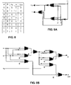
FIGS. 8, 9A and 9B show the truth table and the structure of two embodiments of a full adder using G4-FET devices.
FIG. 10 shows a definition of a parity function.
FIG. 11 shows a parity function circuit comprising G4-FET devices.
FIG. 12 shows a further perspective view of the G4-FET structure, similar to the one of FIG. 3.
FIG. 13 shows a DC configuration of the SOI router in accordance with the present disclosure.
FIGS. 14A-14C show simultaneous drain current variation of an inversion-mode partially-depleted PMOSFET and a buried-channel NMOSFET as a function of front-gate voltage, VG (VD1=−0.1 V, VD2=1.25 V) as shown in FIG. 14A, drain voltage, VD1 (VG=−1 V, VD2=1.25 V) as shown in FIG. 14B, and drain voltage, (VG=−1 V, VD1=−50 mV) as shown in FIG. 14C.
FIG. 15 shows a simultaneous signal transfer from D1 to S1 in lateral direction and from D2 to S2 in perpendicular direction.
FIGS. 16A and 16B show cross-talk between the lateral and perpendicular channels: interference of VD2 signal to channel 1 (FIG. 16A) and interference of VD1 signal to channel 2 (FIG. 16B).
FIG. 17 shows a circuit illustrating the uniform computing and routing capability of a G4-FET device.
DETAILED DESCRIPTION
FIG. 1 depicts an n-channel G4-FET. The G4-FET is constructed from a p-channel MOSFET structure on partially-depleted SOI CMOS technology that has two independent body contacts, one on each side. These body contacts are used as source and drain for the transversal n-channel JFET associated with the structure. The standard MOSFET structure's source and drain are promoted as lateral junction gates for the transversal JFET and used to modulate the conductive path. The maximum extension of the conductive path corresponds to the gate length of the original MOSFET, whereas the JFET channel length is defined by adjusting the width of the MOSFET. Thus, G4-FET gate length is defined by MOFSET drawn gate width and G4-FET gate width is determined by MOSFET drawn gate length. Multiple gate fingers can be readily added in layout to increase the G4-FET's total gate width. No specialized processing is required to manufacture the device.
The G4-FET's operational characteristics have been presented in [References 1-3]. As shown in FIG. 1, the channel of the G4-FET is within the body of the drawn MOSFET structure. Thus, an inversion-mode p-channel MOSFET structure provides an accumulation/depletion-mode n-channel G4-FET. The G4-FET's drain current is composed of majority carriers and flows in a perpendicular direction to that of what would be an inversion-mode MOSFET. The top poly gate and the back gate (substrate) can still be used to modulate the channel current through MOS field effect. The lateral junction gates have a JFET like action, narrowing the channel and modulating the effective doping. Control of the G4-FET's conduction channel will be further enhanced with CMOS technology scaling as the separation between the two junction-gates shrinks.
FIG. 2B describes the logical function of G4-FET gate. Note that this is a 3-input gate, as also shown in FIG. 2A.
To describe the function of this gate in terms of known Boolean functions, first note that the output of a Majority gate is 1 if more than half of its inputs are 1. Thus the function of the G4-FET, as a logic device, is indeed the inverse of a majority gate and hence it is a Not-Majority gate.
Two parameters of the G4-FET, which are critical to its operation as a Not-Majority gate, are its width W and length L. These parameters are defined in FIG. 3. A specific Wmin is required to ensure that the switching on G4-FET logic device can only be switched ‘on’ when any two of its inputs are ‘high’. For W less than this value, a logic high input at any one of its three inputs can turn on the G4-FET. However a maximum W will determine if it is possible to switch the state of the G4-FET. If W is too large, then none of the inputs can cause the G4-FET to switch states. The parameter L determines the current handling capability of the G4-FET, where L is inversely proportional with the current of the G4-FET. Therefore, smaller L will reduce the switching speed of the logic circuit.
The voltage levels required for turning off switching the output state of the G4-FET logic device are also function of the device size, JFET switching voltages are not the same as the voltage level for the switching of the poly gate. Level translators are necessary to convert the output voltage level of the logic stage to input level of the next stage. These level translators are already included in the circuit of FIG. 1.
To explore the computational power of the G4-FET logic device, the Applicants first demonstrate the implementation of the basic Boolean gates by using G4-FET gate. FIG. 4 shows three ways to implement a NOT gate (inverter) by using G4-FET. FIG. 5 shows two ways to implement an AND gate by using G4-FET. FIG. 6 shows two ways to implement an OR gate by using G4-FET.
The above constructions clearly show that the G4-FET (by itself) is a universal gate, since either of the sets {Not, AND} or {Not, OR} is universal. This means that, in principal, the G4-FET logic device is capable of performing any computation.
One of the advantages of the G4-FET structure as a logic gate is that one of its three inputs can be used as a control bit to generate a programmable 2-bit gate. As seen in FIG. 7, by fixing the control bit to 0 or 1, the G4-FET logic device acts as a NAND or NOR gate, respectively. This is another indication that G4-FET is a universal logic gate, just as NAND and NOR are such gates.
The full-adder circuit adds three one-bit binary numbers (a, b, cin) and outputs two one-bit binary numbers: sum (s) and carry (cout), according to the table shown in FIG. 8.
FIG. 9A shows an implementation of the full adder by using 3 G4-FET logic devices and 2 inverters. Note that, to the best of our knowledge, the best implementation of full adder based on basic Boolean gates, uses 9 NAND gates and 4 inverters.
Analyzing the behavior of this circuit reveals the power of the programmable G4-FET logic device. The fact that the functionality of this gate switches between NAND and NOR, depending on the values of its inputs, makes it possible to implement the full adder with a significantly smaller numbers of gates.
FIG. 9B shows a further embodiment of a full adder in accordance with the present disclosure, where nine G4-FET devices with constant mode inputs are used.
In accordance with the present disclosure, circuits based on G4-FET devices for parity functions are provided. A parity function is defined in FIG. 10. FIG. 11 shows a parity function based on G4-FET devices. Only three G4-FET devices are required. A recursive contruction provides a G4-FET based circuit for the function parity(n) with 3(n−1)/2 devices and 2(n−1)/2 inverters. Thus, this circuit needs at most 11n transistors. On the contrary, the optimal NOR-based circuit for the parity(n) function requires 4(n−1) NOR gates, for a total of 16n-4 transistors.
As also explained in the introductory section of the present application, the G4-FET can also function as a unique router device offering coplanar crossing of signal paths that are isolated and perpendicular to one another.
VLSI technology has made possible the integration of many functional components (processors, memory, etc.) into a single chip. In VLSI design, memory and processing are relatively cheap and the main emphasis of the design is on reducing the overall interconnection complexity since data routing costs dominate the power, time, and area required to implement computation. Communication between functional components is costly because wires occupy the most space within a VLSI system and tend to dictate the achievable clock speed. In fact, much of the complexity (and hence the cost) of VLSI design results from minimization of data routing. The main difficulty in VLSI routing is that the crossing of the lines carrying data, instruction, control, etc., is not possible in a single plane of the VLSI chip. At present, wherever two separate wires in a VLSI circuit must cross each other, the wires must not be in the same plane; that is, there must be a layer of electrical insulation between them. Moreover, it is well known that the optimization of VLSI routing is a very computationally challenging problem and, in fact, different versions of this problem are intractable, e.g., [Reference 4].
The basic challenge of VLSI design is that as the number of devices increases, the number of interconnections as well as the area used for these interconnections increases. Due to the dominance of interconnect in the overall delay on chip, today's floorplanning techniques also try to minimize global connectivity and critical net lengths. The current VLSI technology solution for this is to introduce additional layers for interconnections. Technologies with as much as seven metal layers are commercially available today [Reference 5]. But this development has introduced several new problems and has led to extensive research on how to improve the efficiency of current routing algorithms. A summary of these problems is given in [Reference 6]:
Interconnection delays: as technology scaling continues to provide faster transistors and therefore faster logic gates with each process generation, the number of interconnects and the length of those interconnects has increased as well, to the point where interconnect delay can exceed gate delay.
Three dimensional routing: the increased number of interconnection layers provides more freedom in routing and three dimensional routing techniques are necessary to take advantage of the extra connection layers.
Generally a connection between the interconnect layers is achieved using a via. Vias are unavoidable if more than one layer is used for routing, and the problems associated with their usage include the following [Reference 7]:
    • Increasing the number of vias on a chip reduces the probability that the chip will be properly fabricated, therefore reducing yield.
    • Every via has an associated resistance (more than the layers it is connecting) that affects the circuit performance.
    • The size of the via is usually larger than the width of the wires. As a result, vias increase routing space.
    • Successful completion rate of routing synthesis within a VLSI system is inversely proportional to the required number of vias.
Therefore minimizing the number of vias is a challenging optimization problem facing VLSI design.
In the present application, the applicants disclose the unique capability of the G4-FET to function as a via to enable coplanar crossing of signal paths. This capability has the potential of alleviating data routing constraints facing VLSI design since it would enable compact implementation of complex interconnection wiring within a plane that has not been previously possible. The Applicants believe that the G4-FET could potentially open a new direction for efficient VLSI design by enabling coplanar signal crossing.
FIG. 12 shows a perspective view of the G4-FET. The G4-FET is an SOI 4-gate transistor [References 2 and 3] that has the same basic structure as the SOI cross-MOSFET used to construct a singe device inverter in [Reference 8], though the cross-MOSFET is somewhat wider. The operation of the SOI cross-MOSFET is based on the sequential use of the inversion-mode and the accumulation-mode MOSFETs, sharing the gate and substrate terminals.
In the present application, the G4-FET is used as a signal routing device by the simultaneous operation of the inversion-mode MOSFET in the lateral direction and the accumulation-mode MOSFET in the perpendicular direction. Both static and dynamic measurements of the G4-FET as a routing device will be shown.
FIG. 13 shows the DC configuration of the router: the drain of the inversion mode p-channel MOSFET is biased to VD1 and the drain of the accumulation-mode n-channel MOSFET is biased to VD2 while the source terminal of both transistors (S1 and S2) are grounded.
As experimentally demonstrated in FIGS. 14A-14C, the two drain currents ID1 and ID2 (that are perpendicular to each other) may flow at the same time. ID1 depends on the minority carriers and flows at the surface in lateral direction while ID2 depends on majority carriers and flows in the middle of the silicon film volume in the perpendicular direction. Surface holes and bulk electrons do not recombine since the front-gate induced depletion region isolates them. The top-gate can modulate both currents (FIG. 14A): ID1 is controlled through regular MOS action while ID2 is modulated by the vertical depletion width modulation. ID2 can be weakly modulated also by VD1 (FIG. 14B) and vice-versa (FIG. 14C). The ID1 (VD2) dependency is explained by the fact that the body voltage of the PMOSFET is changing between 0 V and VD2, which means that the threshold voltage of the PMOS increases in the S2 to D2 direction. When ID2 saturates, this dependency vanishes (FIG. 14C) because any VD2 increase beyond the saturation voltage drops basically in the pinch-off region. On the other hand, as VD1 becomes more negative, the D1/body junction depletion region extends more into the body, decreasing the channel width and drain current (ID2) of the NMOS (FIG. 14B).
The router operation is tested by simultaneously applying “signals” to drains D1 and D2 and by probing S1 and S2, which are then left floating. Due to the strong length-width asymmetry of the structure (for PMOS: W=3.4 μm, L=0.35 μm), ID2 was much lower than ID1 and was unable to drive the probe capacitance. Therefore it had to be supported by the extra electrons accumulated at the back interface by applying 40V to the substrate. VD1 and VD2 were 1 V peak-to-peak square-waves with −1 V and 1 V offset, respectively. The front surface was kept in strong inversion with VG=−3 V.
FIG. 15 shows the simultaneous and successful transfer of a 50 kHz signal from D1 to S1 and a 10 kHz signal from D2 to S2.
In FIGS. 16A and 16B, the interference between the two channels (cross-talk) is illustrated by applying two signals with relatively large difference in frequency. FIG. 16A shows the “notches” in 1 MHz VD1 signal, induced by the 10 kHz VD2 signal. Likewise a 1 kHz VD1 square-wave affects a 40 kHz VD2 signal in a similar way (FIG. 16B). In both cases the observed distortions are explained by the dynamic threshold voltage change of the transistor conducting the HF signal, as induced by the low-frequency signals. Note that in each case the cross-talk interference seems well within conventional noise margin levels, thus preserving each signal's information integrity.
In accordance with the teachings of the present disclosure, the G4-FET device can be used both as a computing device and as a routing device, as shown, by way of example, in FIG. 17, where G4- FET devices 1, 2, 3, 4 and 5 are shown. In particular, devices 1, 2, 4 and 5 are used for computation (e.g., implementation of some logic functions), while device 3 is used for data routing. Signals O1 and O2, representing the results of the computation performed by devices 1 and 2 are routed by device 3 and fed to devices 4 and 5 as input for further computation. Routing device 3 is a G4-FET operating in accordance with the embodiment explained with reference to FIGS. 13-16, so that line crossing in a plane occurs.
While several illustrative embodiments of the invention have been shown and described above, numerous variations and alternative embodiments will occur to experts. Such variations and alternative embodiments are contemplated and can be made without departing from the scope of the invention as defined in the appended claims.
REFERENCES
  • [1] B. J. Blalock, S. Cristoloveanu, B. M. Dufrene, F. Allibert, and M. M. Mojarradi, The Multiple-Gate MOS-JFET Transistor, Int. J. of High Speed Electronics and Systems, 12, 2 (2002), 511-520.
  • [2] Cristoloveanu, B. Blalock, F. Allibert, B. M. Dufrene, and M. M. Mojarradi, The Four-Gate Transistor, Proceedings of the 2002 European Solid-State Device Research Conf (Firenze, Italy, September 2002). 2002, 323-326.
  • [3] B. Dufrene, K. Akarvardar, S. Cristoloveanu, B. J. Blalock, P. Gentil, E. Kolawa, M. M. Mojarradi, Investigation of the Four Gate Action in G4-FETs, IEEE Trans. on Electron Devices, 51, 11 (November 2004), 1931-1935.
  • [4] R. Greenberg, J. JáJá, and S. Krishnamurthy, On the Difficulty of Manhattan Channel Routing, Information Processing Letters, vol. 44, no. 5, pp. 281-284, 1992.
  • [5] W. Chen (Ed.), The VLSI Handbook, CRC Press, 2000.
  • [6] N. Sherwani, Algorithms for VLSI physical design automation, 2nd ed., Kluwer Academic Publishers, Assinipi Park, 1995.
  • [7] S. Fang, K. Chang, W. Feng, and S. Chen, Constrained via minimization with practical considerations for multi-layer VLSI/PCB routing problems, ACM/IEEE Design Automation Conference, pp. 60-65, 1991.
  • [8] M. H. Gao, S. H. Wu, J. P. Colinge, C. Claeys, and G. Declerck, “Single device inverter using SOI cross-MOSFETs,” Proc. IEEE Int. SOI Conf., 1991, p. 138.

Claims (3)

1. An AND logic gate comprising:
a first four-gate field emitter transistor (G4-FET) having three inputs and one output; and
a second G4-FET having three inputs and one output, wherein:
one of the inputs of the first G4-FET has a low logic value;
a first input of the second G4-FET has a logic value which is opposite to a logic value of
a second input of the second G4-FET; and
a third input of the second G4-FET is connected to the output of the first G4-FET.
2. An OR logic gate comprising:
a first four-gate field emitter transistor (G4-FET) having three inputs and one output; and
a second G4-FET having three inputs and one output, wherein:
one of the inputs of the first G4-FET has a high logic value;
a first input of the second G4-FET has a logic value which is opposite to a logic value of
a second input of the second G4-FET; and
a third input of the second G4-FET is connected to the output of the first G4-FET.
3. A four-gate field emitter transistor (G4-FET) having three inputs and one output, wherein one of the inputs acts as a control bit to generate a programmable 2-bit gate and wherein:
when said one of the inputs has a low logic value the output is an inverse of an AND of the other two inputs; and
when said one of the inputs has a high logic value the output is an inverse of an OR of the other two inputs.
US11/377,935 2005-03-18 2006-03-15 Universal programmable logic gate and routing method Expired - Fee Related US7514964B2 (en)

Priority Applications (1)

Application Number Priority Date Filing Date Title
US11/377,935 US7514964B2 (en) 2005-03-18 2006-03-15 Universal programmable logic gate and routing method

Applications Claiming Priority (3)

Application Number Priority Date Filing Date Title
US66310305P 2005-03-18 2005-03-18
US67800605P 2005-05-04 2005-05-04
US11/377,935 US7514964B2 (en) 2005-03-18 2006-03-15 Universal programmable logic gate and routing method

Publications (2)

Publication Number Publication Date
US20070008013A1 US20070008013A1 (en) 2007-01-11
US7514964B2 true US7514964B2 (en) 2009-04-07

Family

ID=37617756

Family Applications (1)

Application Number Title Priority Date Filing Date
US11/377,935 Expired - Fee Related US7514964B2 (en) 2005-03-18 2006-03-15 Universal programmable logic gate and routing method

Country Status (1)

Country Link
US (1) US7514964B2 (en)

Cited By (2)

* Cited by examiner, † Cited by third party
Publication number Priority date Publication date Assignee Title
US20130232459A1 (en) * 2012-03-05 2013-09-05 Synopsys, Inc. Atpg and compression by using majority gates
US11515318B2 (en) * 2019-02-11 2022-11-29 Intel Corporation 3D floating-gate multiple-input device

Families Citing this family (13)

* Cited by examiner, † Cited by third party
Publication number Priority date Publication date Assignee Title
US7629812B2 (en) * 2007-08-03 2009-12-08 Dsm Solutions, Inc. Switching circuits and methods for programmable logic devices
US7927938B2 (en) * 2007-11-19 2011-04-19 Micron Technology, Inc. Fin-JFET
US8796777B2 (en) * 2009-09-02 2014-08-05 Qualcomm Incorporated Fin-type device system and method
FR2982421A1 (en) * 2011-11-09 2013-05-10 Soitec Silicon On Insulator Semiconductor device for use on semiconductor on insulator substrate, has grid whose back area is formed in massive substrate under insulating layer, where insulating layer electrically isolates back area of grid from semiconductor body
FR2989218A1 (en) * 2012-04-10 2013-10-11 St Microelectronics Sa METHOD FOR PRODUCING AN ELECTRONIC DEVICE BY ASSEMBLING SEMICONDUCTOR BLOCKS AND DEVICE THEREOF
FR3001084B1 (en) * 2013-01-16 2016-04-15 Commissariat Energie Atomique TRANSISTOR WITH GRID AND MASS PLAN COUPLES
US9728636B2 (en) * 2014-04-01 2017-08-08 Northwestern University System and method for threshold logic with electrostatically formed nanowire transistors
CN103956383B (en) * 2014-04-28 2018-04-20 中国科学院宁波材料技术与工程研究所 A kind of transistor based on more top gate structures
US11956952B2 (en) 2015-08-23 2024-04-09 Monolithic 3D Inc. Semiconductor memory device and structure
US11296115B1 (en) 2015-10-24 2022-04-05 Monolithic 3D Inc. 3D semiconductor device and structure
US11114464B2 (en) 2015-10-24 2021-09-07 Monolithic 3D Inc. 3D semiconductor device and structure
US10783297B2 (en) * 2017-10-13 2020-09-22 Bank Of America Corporation Computer architecture for emulating a unary correlithm object logic gate
US10783298B2 (en) * 2017-10-13 2020-09-22 Bank Of America Corporation Computer architecture for emulating a binary correlithm object logic gate

Citations (2)

* Cited by examiner, † Cited by third party
Publication number Priority date Publication date Assignee Title
US5543643A (en) * 1995-07-13 1996-08-06 Lsi Logic Corporation Combined JFET and MOS transistor device, circuit
US6180984B1 (en) 1998-12-23 2001-01-30 Honeywell Inc. Integrated circuit impedance device and method of manufacture therefor

Family Cites Families (10)

* Cited by examiner, † Cited by third party
Publication number Priority date Publication date Assignee Title
US4253073A (en) * 1978-08-17 1981-02-24 Communications Satellite Corporation Single ground plane interdigital band-pass filter apparatus and method
US5204555A (en) * 1990-04-05 1993-04-20 Gazelle Microcircuits, Inc. Logic array having high frequency internal clocking
US5941974A (en) * 1996-11-29 1999-08-24 Motorola, Inc. Serial interface with register selection which uses clock counting, chip select pulsing, and no address bits
JP3037252B2 (en) * 1998-01-28 2000-04-24 日本電気アイシーマイコンシステム株式会社 Address selection circuit
US6778042B2 (en) * 2000-10-30 2004-08-17 Kabushiki Kaisha Toshiba High-frequency device
JP4707255B2 (en) * 2001-04-26 2011-06-22 ルネサスエレクトロニクス株式会社 Semiconductor memory device
EP1298757A1 (en) * 2001-09-29 2003-04-02 Marconi Communications GmbH High frequency bandpass filter and tuning method thereof
WO2003052930A1 (en) * 2001-12-14 2003-06-26 Mitsubishi Denki Kabushiki Kaisha Filter circuit
US6762660B2 (en) * 2002-05-29 2004-07-13 Raytheon Company Compact edge coupled filter
JP4732709B2 (en) * 2004-05-20 2011-07-27 株式会社半導体エネルギー研究所 Shift register and electronic device using the same

Patent Citations (2)

* Cited by examiner, † Cited by third party
Publication number Priority date Publication date Assignee Title
US5543643A (en) * 1995-07-13 1996-08-06 Lsi Logic Corporation Combined JFET and MOS transistor device, circuit
US6180984B1 (en) 1998-12-23 2001-01-30 Honeywell Inc. Integrated circuit impedance device and method of manufacture therefor

Non-Patent Citations (9)

* Cited by examiner, † Cited by third party
Title
Blalock. B.J., et al., "The Multiple Gate MOS-JFET Transistor," Int. Journal of High Speed Electronics and Systems, 12, 2, pp. 511-520 (2002), month unk.
Cristoloveanue, B., et al., "The Four-Gate Transistor," Proceedings of the 2002 European Solid-State Device Research Conf., pp. 323-326 (2002), month unk.
Dufrene, B., et al., "Investigation of the Four-Gate Action in G4 -FETs,"IEEE Trans. On Electron Devices, 51, 11, pp. (Nov. 2004).
Fang, S., et al., "Constrained via minimization with practical considerations for multi-layer VLS/PCB routing problems," ACM/IEEE Design Automation Conference, pp. 60-65 (1991), month unk.
Fijany, A., et al., "The G4-FET: A Universal and Programmable Logic Gate," GLSVLSI '05, (Apr. 17-19, 2005).
Gao, M.H., et al., "Single device: inverter using SOI corss-MOSFETS," Proc. IEEE Int.SOI Conf., p. 138 (1991), month unk.
Greenberg, R., et al., "On the Difficulty of Manhattan Channel Routing," Information Processing Letters, vol. 44, No. 5, pp. 281-284 (1992), month unk.
K. Akarvardar et al. IEEE 2006. Low-Frequency Noise in SOI Four-Gate Transistors, pp. 1-7. *
S. Cristoloveanu, Journal of The Korean Physical Society, vol. 45, No. 5, Nov. 2004, pp. 1189-1192. *

Cited By (3)

* Cited by examiner, † Cited by third party
Publication number Priority date Publication date Assignee Title
US20130232459A1 (en) * 2012-03-05 2013-09-05 Synopsys, Inc. Atpg and compression by using majority gates
US8549372B2 (en) * 2012-03-05 2013-10-01 Synopsys, Inc. ATPG and compression by using majority gates
US11515318B2 (en) * 2019-02-11 2022-11-29 Intel Corporation 3D floating-gate multiple-input device

Also Published As

Publication number Publication date
US20070008013A1 (en) 2007-01-11

Similar Documents

Publication Publication Date Title
US7514964B2 (en) Universal programmable logic gate and routing method
US7557608B2 (en) Passgate structures for use in low-voltage applications
EP1304803B1 (en) Programmable logic device comprising silicon-on-insulator transistors
US20040196684A1 (en) Semiconductor integrated circuit device, storage medium on which cell library is stored and designing method for semiconductor intergrated circuit
JPS5837637B2 (en) Electrically switchable read-only storage
JP2002033399A (en) Semiconductor integrated circuit and its manufacturing method
Ono et al. Binary adders of multigate single-electron transistors: Specific design using pass-transistor logic
JP2008509604A (en) Enhanced pass gate structure to reduce leakage current
WO2011107355A1 (en) Data-path cell on an seoi substrate with a back control gate beneath the insulating layer
US6380765B1 (en) Double pass transistor logic with vertical gate transistors
EP0151870B1 (en) Gate array integrated circuit using schottky-barrier fets
US6429492B1 (en) Low-power CMOS device and logic gates/circuits therewith
US7652330B1 (en) Independently-double-gated combinational logic
Baldauf et al. Vertically integrated reconfigurable nanowire arrays
US11043592B2 (en) Antiferromagnet field-effect based logic circuits including spin orbital coupling channels with opposing preferred current paths and related structures
EP0046197B1 (en) Fet convolved logic
CN107452740B (en) Integrated circuit with spare unit
Fijany et al. The G4-FET: A universal and programmable logic gate
KR100343147B1 (en) Semiconductor device and signal processing system having SOI MOS transistor
US6563367B1 (en) Interconnection switch structures
KR20050103195A (en) Organic field effect transistor and integrated circuit
JP2000029665A (en) Semiconductor integrated circuit
JP2852051B2 (en) Complementary clock donand circuit
US6570409B2 (en) Current steering logic circuits
Liu et al. Design of CNTFET-based reconfigurable logic gate

Legal Events

Date Code Title Description
AS Assignment

Owner name: NASA, DISTRICT OF COLUMBIA

Free format text: CONFIRMATORY LICENSE;ASSIGNOR:CALIFORNIA INSTITUTE OF TECHNOLOGY;REEL/FRAME:018129/0105

Effective date: 20060628

AS Assignment

Owner name: CALIFORNIA INSTITUTE OF TECHNOLOGY, CALIFORNIA

Free format text: ASSIGNMENT OF ASSIGNORS INTEREST;ASSIGNORS:FIJANY, AMIR;VATAN, FARROKH;MOJARRADI, MOHAMMAD M.;AND OTHERS;REEL/FRAME:018310/0897;SIGNING DATES FROM 20060905 TO 20060913

Owner name: UNIVERSITY OF TENNESSEE RESEARCH FOUNDATION, TENNE

Free format text: ASSIGNMENT OF ASSIGNORS INTEREST;ASSIGNORS:FIJANY, AMIR;VATAN, FARROKH;MOJARRADI, MOHAMMAD M.;AND OTHERS;REEL/FRAME:018310/0897;SIGNING DATES FROM 20060905 TO 20060913

FPAY Fee payment

Year of fee payment: 4

REMI Maintenance fee reminder mailed
LAPS Lapse for failure to pay maintenance fees
STCH Information on status: patent discontinuation

Free format text: PATENT EXPIRED DUE TO NONPAYMENT OF MAINTENANCE FEES UNDER 37 CFR 1.362

FP Expired due to failure to pay maintenance fee

Effective date: 20170407