US7508043B2 - Sensor for analyzing a sample by utilizing localized plasmon resonance - Google Patents
Sensor for analyzing a sample by utilizing localized plasmon resonance Download PDFInfo
- Publication number
- US7508043B2 US7508043B2 US11/224,279 US22427905A US7508043B2 US 7508043 B2 US7508043 B2 US 7508043B2 US 22427905 A US22427905 A US 22427905A US 7508043 B2 US7508043 B2 US 7508043B2
- Authority
- US
- United States
- Prior art keywords
- sensor
- sensor chip
- pits
- chip
- measuring light
- Prior art date
- Legal status (The legal status is an assumption and is not a legal conclusion. Google has not performed a legal analysis and makes no representation as to the accuracy of the status listed.)
- Expired - Fee Related, expires
Links
Images


Classifications
-
- G—PHYSICS
- G01—MEASURING; TESTING
- G01N—INVESTIGATING OR ANALYSING MATERIALS BY DETERMINING THEIR CHEMICAL OR PHYSICAL PROPERTIES
- G01N21/00—Investigating or analysing materials by the use of optical means, i.e. using sub-millimetre waves, infrared, visible or ultraviolet light
- G01N21/17—Systems in which incident light is modified in accordance with the properties of the material investigated
- G01N21/55—Specular reflectivity
- G01N21/552—Attenuated total reflection
- G01N21/553—Attenuated total reflection and using surface plasmons
- G01N21/554—Attenuated total reflection and using surface plasmons detecting the surface plasmon resonance of nanostructured metals, e.g. localised surface plasmon resonance
Definitions
- the present invention relates to a sensor for detecting the localized plasmon resonance state of a metal particle surface by light and analyzing a sample present near metal particles, a method of analyzing a sample by the use of the sensor, a sensor chip employed in the sensor, and a method of manufacturing the sensor chip.
- a sensor in which a fine structure, having a layer of metal particles fixed on the surface of a dielectric or semiconductor, etc., is employed as a sensor chip to measure the refractive index, etc., of a sample by making use of localized plasmon resonance.
- This sensor basically includes means for irradiating measuring light to the metal particles of the sensor chip, and light detection means for detecting the intensity of the measuring light transmitted through or reflected at the metal particle layer.
- the aforementioned sensor if measuring light is irradiated onto the metal particle layer, localized plasmon resonance takes place at a particular wavelength, and consequently, the scattering and absorption of the measuring light increase appreciably. Therefore, if the sensor is set so the intensity of the measuring light transmitted through or reflected at the metal particle layer can be detected, the occurrence of localized plasmon resonance can be confirmed by observing that the intensity of the detected light attenuates sharply.
- the wavelength where localized plasmon resonance takes place, and the degree of the scattering and absorption of measuring light, depend upon the refractive index of a substance present near metal particles. In other words, as the refractive index becomes greater, the resonance peak wavelength shifts to a longer wavelength side and the scattering and absorption of measuring light increase. Therefore, by irradiating measuring light to a metal particle layer with a sample arranged near the metal particle layer and then detecting the intensity of the measuring light transmitted through or reflected at the metal particle layer, the refractive index of the sample and properties of the sample relating to it can be measured.
- the aforementioned resonance peak wavelength shift may be detected.
- monochromatic light the aforementioned resonance peak wavelength shift, and a change in the light intensity associated with a change in the scattering and absorption of the measuring light, may also be detected.
- the measuring light transmitted through the metal particle layer may be detected by arranging a photodetector on a side opposite to the measuring-light irradiation side with respect to the metal particles, or the measuring light reflected at the metal particles may be detected by arranging the photodetector on the same side as the measuring-light irradiation side with respect to the metal particles.
- the substrate for fixing the metal particle layer is formed from a reflective material, the measuring light transmitted through the metal particles is reflected at the substrate and therefore the light transmitted through the metal particles can also be detected.
- a sensing medium to bind with a particular substance is fixed near the metal particles of the sensor chip, the refractive index of the particular substance near the metal particles changes, depending on the presence or absence of the binding between the sensing medium and the particular substance.
- the particular substance and sensing medium combination are various antigens and an antibody, etc.
- a conventional sensor chip used in a sensor making use of the localized plasmon resonance is shown in Japanese Unexamined Patent Publication No. 2000-356587 by way of example.
- this sensor chip a single layer of metal colloid is formed on one surface of a substrate.
- a sensor chip comprises an anodic alumina layer with a plurality of pits in one surface thereof, and metal particles with which the pits are filled up.
- This sensor chip can also be used in the aforementioned sensor.
- the aforementioned metal particles comprise metal particles in the form of lumps, having nearly the same three-dimensional dimensions. Examples of the anodic alumina layer with a plurality of pits are also disclosed in Japanese Unexamined Patent Publication. No. 11 (1999)-200090 and “High Regular Metal Nanohole Array,” by H. Masuda, Solid Physics, Vol. 31, No. 5, pp. 493-498, 1996.
- a change in the resonance peak wavelength and a change in the intensity of the measuring light must be detected before and after the supply of the sample to the metal particle layer, as described above.
- the resonance peak wavelength and the intensity of the measuring light will change even if the incidence angle of the measuring light with respect to the metal particle layer changes.
- the incidence angles need to coincide before and after the supply of the sample to the metal particle layer. For that reason, throughout the time from when a sample is supplied to the metal particle layer to when an analysis of the sample is completed, the sensor chip is fixed to prevent the occurrence of a shift in the sensor chip that will cause a shift in the incidence angle.
- the sensing chip has to be fixed for a long period of time until the reaction between them starts and is completed.
- the sensor chip is fixed, that is, until the aforementioned reaction is completed, it is impossible to use the sensor to analyze another sample. Because of the waiting time, the efficiency of sample analysis is decreased.
- an aspect of the present invention provides a sensor in which there is no possibility that the efficiency of sample analysis will be reduced by fixing a sensor chip for a long period of time, and a method of analyzing a sample by the use of the sensor.
- Another aspect of the invention provides a sensor chip employed in the aforementioned sensor and a method of manufacturing the sensor chip.
- a sensor chip for use in a sensor for detecting a localized plasmon resonance state of a metal particle surface and analyzing properties of a sample present near metal particles.
- the sensor chip of the present invention comprises two major components: (1) a support with a plurality of pits individually and independently formed in one surface thereof so that they extend toward an interior thereof; and (2) rods of metal particles, whose aspect ratio (the ratio between diameter and length) is not 1, respectively held in the plurality of pits so that an end surface of each rod is exposed at the one surface of the support and a longitudinal side surface of each rod is covered with the support.
- a method of manufacturing the sensor chip of the present invention comprises the steps of (a) forming on one surface of a support an anodic alumina layer having a plurality of through pits extending in a direction substantially perpendicular to the one surface; (b) forming in the one surface of the support a plurality of pits corresponding to the through pits and extending in the direction of the depth of the support, by etching the support with the anodic alumina layer as a mask; (c) removing the anodic alumina layer; and (d) filling up the pits of the support with rods of metal particles respectively, by depositing metal particles on the one surface of the support and within the pits and then removing the metal particles deposited on the one surface.
- a first sensor employing the sensor chip of the present invention described above.
- the first sensor comprises five major components: (1) means for irradiating measuring light having a predetermined wavelength band to the rods of metal particles of the sensor chip; (2) sensor-chip hold means for holding the sensor chip so that the longitudinal axes of the metal particle rods are inclined with respect to an electric field direction of the measuring light, and so that the angle of inclination can be freely changed; (3) drive means for driving the sensor-chip hold means so that the angle of inclination is changed; (4) light detection means for spectrally detecting an intensity of the measuring light transmitted through the metal particle rods or reflected at the metal particle rods; and (5) control means for setting a direction of the sensor-chip hold means so that the angle of inclination is fixed, by controlling operation of the drive means based on the intensity detected by the light detection means.
- a second sensor employing the sensor chip of the present invention described above.
- the second sensor comprises four major components: (1) means for irradiating measuring light having a predetermined wavelength band to the rods of metal particles of the sensor chip; (2) sensor-chip hold means for holding the sensor chip so that the longitudinal axes of the metal particle rods are inclined with respect to an electric field direction of the measuring light, and so that the angle of inclination can be freely changed; (3) light detection means for spectrally detecting an intensity of the measuring light transmitted through the metal particle rods or reflected at the metal particle rods; and (4) display means for displaying the intensity detected by the light detection means.
- a method of analyzing a sample by employing the aforementioned second sensor comprises the steps of: (a) irradiating measuring light to the metal particles of the sensor chip before and after the sample is supplied; (b) storing an intensity of the measuring light measured at a first particular wavelength of a wavelength band of the measuring light, displayed on the display means when the measuring light is irradiated before sample supply; (c) adjusting an angle of inclination of the sensor chip held by the sensor-chip hold means so that an intensity of the measuring light at the first particular wavelength, displayed on the display means after sample supply, coincides with the stored intensity; and (d) analyzing the sample, based on the intensity of the measuring light measured at a second particular wavelength different from the first particular wavelength, displayed on the display means.
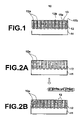
- FIG. 1 is a schematic side view showing a sensor chip constructed in accordance with a first embodiment of the present invention
- FIG. 2 which includes FIGS. 2A and 2B , is a simplified diagram used to explain a method of manufacturing the sensor chip shown in FIG. 1 ;
- FIG. 3 is a schematic side view showing a sensor including the sensor chip shown in FIG. 1 ;
- FIG. 4 is a graph showing the spectral intensity characteristic of the measuring light detected by the sensor shown in FIG. 3 ;
- FIG. 5 which includes FIGS. 5A to 5E , is a schematic side view showing how a sensor chip is manufactured in accordance with a second embodiment of the present invention.
- FIG. 6 is a schematic side view showing a sensor chip constructed in accordance with a third embodiment of the present invention.
- FIG. 1 there is shown a sensor chip 10 constructed in accordance with a first embodiment of the present invention.
- the sensor chip 10 shown in the figure comprises a layer of anodic alumina 12 as a support formed on an aluminum substrate 11 , and gold particles 13 with which a great number of pits 12 a formed in one surface of the anodic alumina 12 are filled up.
- each pit 12 a is about 200 nm or less as an example and the inside diameter is, for example, about a few nm to 100 nm. Since the gold particles 13 are held in the pits 12 a , they are shaped as elongated rods. The end surface 13 a of each gold particle rod 13 is exposed at the one surface 12 b of the anodic alumina 12 , while the longitudinal side surface 13 b is covered with the anodic alumina 12 .
- FIG. 2 there is shown a method of manufacturing the aforementioned sensor chip 10 .
- an aluminum substrate 11 with a layer of anodic alumina 12 formed on the surface is first prepared.
- one surface 12 b of the anodic alumina 12 layer in which pits 12 a are formed is electroplated with gold.
- the pits 12 a in the anodic alumina 12 are filled up with gold particles 13 .
- electroplating conditions are suitably controlled, only pits 12 a can be filled up with gold particles 13 , without plating the surface 12 b of the anodic alumina 12 with gold. Instead of electroplating, the pits 12 a can also be filled up with gold particles 13 by vapor deposition.
- metal particle rods may be formed from other metals such as silver, copper, aluminum, etc.
- gold is the particularly preferred material in view of the following points. That is, because gold is malleable and ductile, vapor deposition can be easily performed even at relatively low temperatures. Gold is also high in corrosion resistance. Therefore, when the sensor chip 10 is used in a sensor to be described later, the sensor is able to have stable properties. The sensor is also made easier to handle when manufactured and used.
- anodic alumina layer 12 on the aluminum substrate 11
- a method of simultaneously advancing generation of an oxide film and dissolution of the generated oxide layer is basically employed in performing an anodic oxidation process on the aluminum substrate 11 in an acid electrolytic solution.
- pits are randomly formed in the surface of an oxide layer formed on the aluminum substrate 11 at the start of the anodic oxidation, by dissolution action by acid. With the progress of the anodic oxidation, some of the pits grow preferentially and are arranged at nearly equal intervals. Because an electric field applied to the pitted portion in the oxide film is higher than that applied to the non-pitted portion, dissolution of the pitted portion is more easily expedited.
- pits 12 a are selectively formed with the growth, while an undissolved portion is formed so as to surround the pits 12 a.
- pits 12 a are regularly arranged and formed. These pits 12 a extend in a direction approximately perpendicular to the surface of the anodic alumina 12 and respectively form cylindrical spaces that are nearly the same in cross section and closed at the bottoms.
- Japanese Unexamined Patent Publication Nos. 2001-9800 and 2001-138300 disclose methods of controlling the positions at which the aforementioned pits are formed.
- dissolution-starting points are formed at the desired positions, for example, by irradiating a focused ion beam to aluminum. After this process, by performing an anodic oxidation process, pits 12 a can be formed at the desired positions. And in irradiating the focused ion beam, if the irradiation quantity, beam diameter, irradiation energy, etc., are controlled, the indentation and composition of the dissolution-starting point can be varied. Therefore, the diameter of each pit 12 a to be finally formed can also be freely controlled.
- a method of arranging the pits 12 a at high density there is a method employing oxalic acid. That is, by employing oxalic acid as an electrolytic solution for anodic oxidation and performing an anodic oxidation process under a constant voltage of about 40 V, pits 12 a can be regularly arranged at high density. Because the regular arrangement of the pits 12 a progresses with the lapse of anodic oxidation time, the pits 12 a can be regularly arranged at high density by performing the anodic oxidation process for a long period of time.
- the diameter, pitch, and depth of the pits 12 a can be relatively freely controlled in the aforementioned manner, gold particles 13 can be formed to an arbitrary uniform size and it becomes possible to arrange them regularly. As a result, if the sensor chip 10 is employed in a sensor described later, the sensitivity can be enhanced and stabilized.
- this sensor comprises six major components: (1) a white light source 21 for irradiating measuring light 20 (e.g., white light) to the gold particle rods 13 of the sensor chip 10 ; (2) sensor-chip hold means 22 for holding the sensor chip 10 so that the longitudinal axis of each gold particle rod 13 is inclined with respect to the electric field direction of the measuring light 20 ; (3) a three-axis revolvable actuator 23 for fixing the sensor-chip hold means 22 thereto; (4) a polychromator 24 for spectrally detecting the intensity of the measuring light 20 reflected at the gold particles 13 ; (5) a control circuit 25 for controlling operation of the actuator 23 based on the intensity measured by the polychromator 24 ; and (6) display means 26 connected to the control circuit 25 and polychromator 24 .
- a white light source 21 for irradiating measuring light 20 (e.g., white light) to the gold particle rods 13 of the sensor chip 10
- sensor-chip hold means 22 for holding the sensor chip 10 so that the longitudinal axis of each gold
- the sensor chip 10 With the anodic alumina 12 upward, the sensor chip 10 is arranged on the sensor-chip hold means 22 .
- the three-axis revolvable actuator 23 can cause the sensor-chip hold means 22 to revolve on x, y, and z axes shown in FIG. 3 . In this manner, the sensor-chip hold means 22 can change in posture. If the posture of the sensor-chip hold means 22 is changed, the angle of inclination of each gold particle rod 13 changes accordingly.
- the measuring light 20 (which is white light) is irradiated onto the sensor chip 10 , it is reflected at the gold particles 13 (see FIG. 1 ).
- the reflected light 20 is detected by polychromator 24 .
- the spectral intensity characteristic of the reflected light is represented by a solid line shown in FIG. 4 . That is, when the measuring light 20 is irradiated onto the gold particles 13 of the anodic alumina 12 , absorption of the measuring light 20 is increased at particular wavelengths ⁇ 1 and ⁇ 2 by localized plasmon resonance. Note that the solid line in FIG. 4 represents absorbance of the measuring light 20 reflected at the anodic alumina 12 before sample supply.
- the wavelengths (resonance peak wavelengths) at which localized plasmon resonance occurs, and the degree of absorption (absorbance) of the measuring light 20 depend upon the refractive index of a substance present around the gold particles 13 . That is, as the refractive index becomes greater, the resonance peak wavelength is shifted to a longer wavelength side and the absorbance increases.
- the first resonance peak wavelength ⁇ 1 shown in FIG. 4 depends on the side surface 13 b of each gold particle rod 13
- the second resonance peak wavelength ⁇ 2 depends on the end surface 13 a of the gold particle rod 13 . Therefore, if a sample is supplied to the anodic alumina 12 , the second resonance peak wavelength ⁇ 2 is shifted as described above and the absorbance at that wavelength increases by ⁇ A.
- the spectral absorption characteristic varies as shown by the broken line in FIG. 4 . The reason is that if a sample is supplied, it adheres to the end surface 13 a of each gold particle rod 13 and the refractive index of the substance in contact with the end surface 13 a changes.
- the first resonance peak wavelength ⁇ 1 is not shifted and the absorbance at that wavelength does not increase. Therefore, if the first resonance peak wavelength ⁇ 1 is shifted or the absorbance at that wavelength increases, the shift or increase is considered to be due to a shift in the angle of inclination of the sensor chip 10 with respect to the measuring light 20 .
- a sample is supplied to the gold particles 13 of the sensor chip 10 .
- the aforementioned sensing medium e.g., one of between an antigen and an antibody
- the refractive index of the medium in contact with the end surface 13 a of each gold particle rod 13 changes due to the binding, while the side surface 13 b of each gold particle rod does not cause any change in the refractive index of the medium.
- the control circuit 25 receives a signal from the polychromator 24 that has detected the intensity of the measuring light 20 reflected at the gold particle rods 13 of the sensor chip 10 , and then calculates the absorbance characteristic shown in FIG. 4 .
- the control circuit 25 detects a shift in the resonance peak wavelength and an increase in the absorbance after sample supply. Based on the wavelength shift and absorbance increase, the control circuit 25 calculates the refractive index of the sample and properties relating to it and displays them on the display means 26 .
- the control circuit 25 calculates the absorbance at that wavelength before sample supply and stores the calculated value in storage means (not shown). For example, if a sensor-chip angle alignment command is input through input means such as a keyboard (not shown) after a sample is supplied to the sensor chip 10 , operation of the three-axis revolvable actuator 23 is controlled so that the absorbance at the first resonance peak wavelength ⁇ 1 measured at the time of the sample supply coincides with the absorbance previously stored in the storage means (not shown).
- the angle of inclination of the sensor chip 10 with respect to the measuring light 20 coincides with the inclination angle arranged before sample supply.
- the sample is analyzed based on the shift in the resonance peak wavelength ⁇ 2 and increase in the absorbance. Therefore, since there is no possibility that errors in measurement will be caused by a shift in the inclination angle of the sensor chip 10 , accuracy in sample analysis can be enhanced.
- the inclination angle of the sensor chip 10 is automatically adjusted by the three-axis revolvable actuator 23 and control circuit 25 so that the absorbance at the first resonance peak wavelength ⁇ 1 , measured at the time of the input of a sensor-chip angle alignment command, coincides with the value of the absorbance previously stored. It is also possible to perform a sensor-chip angle adjustment by hand. In that case, an actuator capable of being operated by hand is used as the three-axis revolvable actuator 23 .
- the absorbance characteristic shown in FIG. 4 is displayed on the display means 26 , and the absorbance at the first resonance peak wavelength ⁇ 1 before sample supply, displayed on the display means 26 , is stored.
- the three-axis revolvable actuator 23 is manually operated so that the absorbance at the first resonance peak wavelength ⁇ 1 displayed on the display means 26 coincides with the stored absorbance.
- the sensor-chip hold means 22 may be operated by drive means capable of being operated only by hand.
- the support of the sensor chip of the present invention can also be formed by other methods.
- FIG. 5 there is shown a sensor chip manufactured in accordance with a second embodiment of the present invention.
- an anodic alumina layer 12 having a plurality of through pits 12 a′ extending in a direction substantially perpendicular to the one surface 41 a .
- the anodic alumina layer 12 shown in FIG. 5 can also be obtained, for example, by removing from the sensor chip 10 shown in FIG. 2 the boundary portion between the aluminum substrate 11 and the anodic alumina layer 12 .
- a plurality of pits 41 b corresponding to the through pits 12 a ′ are formed in the transparent dielectric substrate 41 and extend in the direction of the depth of the transparent dielectric substrate 41 .
- This etching process is performed by employing oxygen or CF 4 as an etchant.
- the anodic alumina 12 used as the mask is removed from the transparent substrate 41 .
- the one surface 41 a of the transparent dielectric substrate 41 is covered with gold by vapor deposition or sputtering.
- gold particles 13 b are deposited on the one surface 41 a of the transparent dielectric substrate 41 and gold particles 13 a are deposited within the pits 41 b of the transparent dielectric substrate 41 .
- the gold particles 13 b on the one surface 41 a of the transparent dielectric substrate 41 are removed as shown in FIG. 5E .
- a sensor chip 40 with the pits 41 b respectively filled up with gold particle rods 13 a is obtained.
- the sensor chip 40 can be a component of the sensor of the present invention, as with the sensor chip 10 shown in FIG. 1 .
- the support of the sensor chip 40 is formed from the transparent dielectric substrate 41 , it is also possible to analyze a sample by irradiating measuring light to the gold particle rods 13 and detecting the measuring light transmitted through the sensor chip 40 .
- FIG. 6 there is shown a sensor chip 50 constructed in accordance with a third embodiment of the present invention.
- This sensor chip 50 is manufactured by employing the anodic alumina layer 12 with through pits 12 a ′ which is used in manufacturing the sensor chip 40 shown in FIG. 5 . That is, if the through pits 12 a in the anodic alumina layer 12 are filled up with gold particles 13 , the sensor chip 50 is obtained. Because measuring light is transmitted through the anodic alumina layer 12 of the sensor chip 50 , it is also possible to analyze a sample by detecting the measuring light transmitted through the sensor chip 50 .
- a plurality of rods of metal particles whose aspect ratio is not 1 are formed so that an end surface of each rod is exposed at one surface of the support and a longitudinal side surface of each rod is covered with the support. If measuring light is irradiated onto the thus-constructed sensor chip so that an electric field direction thereof is inclined with respect to the longitudinal axis of each rod, and an absorption spectrum from the sensor chip is examined, a first absorption peak depending on the end surface of the metal particle rod and a second absorption peak depending on the side surface of the metal particle rod occur at different wavelengths, because the measuring light is irradiated onto both the end surface and the side surface.
- localized plasmon resonance takes place only at a longer wavelength side (e.g., wavelength ⁇ 2 shown in FIG. 4 described later) if the electric field direction of the measuring light (i.e., the direction of the electric field vector) coincides with the direction of the longitudinal axis of the metal particle rod, and localized plasmon resonance takes place only at a shorter wavelength side (e.g., wavelength ⁇ 1 shown in FIG. 4 ) if the electric field direction of the measuring light coincides with the direction of the diameter of the metal particle rod.
- a longer wavelength side e.g., wavelength ⁇ 2 shown in FIG. 4 described later
- the electric field direction of the measuring light i.e., the direction of the electric field vector
- a shorter wavelength side e.g., wavelength ⁇ 1 shown in FIG. 4
- the wavelengths at which localized plasmon resonance takes place are determined according to the boundary conditions of the interface between the metal particle rod in the longitudinal axis direction and the surrounding medium and to the length of the metal particle rod.
- the aforementioned “absorption peak depending on the end surface of a metal particle rod” indicates an absorption peak occurring in this case.
- the wavelengths at which localized plasmon resonance takes place are determined according to the boundary conditions of the interface between the metal particle rod in the diameter direction and the surrounding medium and to the diameter of the metal particle rod.
- the aforementioned “absorption peak depending on the side surface of a metal particle rod” indicates an absorption peak occurring in this case.
- the end surface of a metal particle rod is exposed at one surface of the support, while the side surface is covered with the support. For this reason, a sample adheres to the rod end surface, but it cannot adhere to the side surface. Therefore, the absorption peak depending on the end surface of a metal particle rod changes before and after sample supply, and based on the change, the refractive index of the sample and properties relating to it can be analyzed. On the contrary, the absorption peak depending on the side surface does not change before and after sample supply.
- the angle of inclination of the sensor chip by the sensor-chip hold means is adjusted so that the intensity of measuring light at the first particular wavelength (at which the absorption peak depending on the side surface of a metal particle rod takes place), displayed on the display means when the measuring light is irradiated after sample supply, coincides with the stored intensity (i.e., the intensity of the measuring light at the first particular wavelength displayed on the display means when the measuring light is irradiated before sample supply), then the inclination angles coincide before and after sample supply.
- the sensor chip can be removed from the sensor-chip hold means. Therefore, while the sensor chip is removed from the sensor-chip hold means, it becomes possible to perform some or all of sample-analyzing operations with another sensor chip. Thus, the efficiency of sample analysis is considerably enhanced.
- the first sensor of the present invention can automatically carry out the same operations as the aforementioned sample analysis method, because it is equipped with control means for setting the direction of the sensor-chip hold means so that the angle of inclination of the longitudinal axis of the metal particle rod with respect to the electric field direction of the measuring light is fixed.
- the sensor chip of the present invention as previously mentioned, a plurality of rods of metal particles are provided so that the end surface of each rod is exposed at one surface of the support and the longitudinal side surface is covered with the support. Therefore, the sensor chip of the present invention can constitute the first or second sensor of the present invention.
- the aforementioned anodic alumina is formed as a metal oxide layer in the surface of aluminum by performing an anodic oxidation process on the aluminum in an acid electrolytic solution.
- pits of about a few nanometers to a few hundred nanometers in diameter are individually and independently formed so that they extend in a direction substantially perpendicular to the surface. They are also arranged at nearly equal intervals. And the diameter, depth, and pitch of the pits can be relatively freely set by controlling anodic oxidation conditions (see the aforementioned “High Regular Metal Nanohole Array,” by H. Masuda, Solid Physics, Vol. 31, No. 5, pp. 493-498, 1996).
- the sensor chip of the present invention is equipped with a plurality of metal particle rods, it is necessary to accurately control the depth of the pits of the support that are to be filled up with the metal particle rods.
- the anodic alumina having the aforementioned properties is extremely preferable as the material of the support constituting this sensor chip.
- the aforementioned anodic alumina may be employed as a layer formed on the surface of an aluminum substrate, or after being removed from the aluminum surface, it may be fixed on another substrate and employed.
- the support with a great number of pits can be very easily fabricated and thus a reduction in cost of the sensor chip can be realized.
- anodic alumina layer having a plurality of through pits extending in a direction substantially perpendicular to the one surface. And in the one surface of the support, there are formed a plurality of pits corresponding to the through pits and extending in the direction of the depth of the support, by etching the support with the anodic alumina layer as a mask. Therefore, the pits can be easily formed and the sensor chip can be efficiently manufactured.
- the aforementioned support may be formed from anodic alumina.
- the aforementioned pits may be formed in the support by an etching process in which anodic alumina with a plurality of pits is used as a mask.
- the maximum dimension of the aforementioned metal particles may be 200 nm or less.
- the metal particles may be formed from one of among gold, silver, copper, and aluminum.
Landscapes
- Chemical & Material Sciences (AREA)
- Engineering & Computer Science (AREA)
- Nanotechnology (AREA)
- Physics & Mathematics (AREA)
- Health & Medical Sciences (AREA)
- Life Sciences & Earth Sciences (AREA)
- Analytical Chemistry (AREA)
- Biochemistry (AREA)
- General Health & Medical Sciences (AREA)
- General Physics & Mathematics (AREA)
- Immunology (AREA)
- Pathology (AREA)
- Investigating Or Analysing Materials By Optical Means (AREA)
Abstract
Description
Claims (5)
Applications Claiming Priority (2)
| Application Number | Priority Date | Filing Date | Title |
|---|---|---|---|
| JP2004265435A JP4361448B2 (en) | 2004-09-13 | 2004-09-13 | Sensor and sample analysis method using the sensor |
| JP265435/2004 | 2004-09-13 |
Publications (2)
| Publication Number | Publication Date |
|---|---|
| US20060055933A1 US20060055933A1 (en) | 2006-03-16 |
| US7508043B2 true US7508043B2 (en) | 2009-03-24 |
Family
ID=36033545
Family Applications (1)
| Application Number | Title | Priority Date | Filing Date |
|---|---|---|---|
| US11/224,279 Expired - Fee Related US7508043B2 (en) | 2004-09-13 | 2005-09-13 | Sensor for analyzing a sample by utilizing localized plasmon resonance |
Country Status (2)
| Country | Link |
|---|---|
| US (1) | US7508043B2 (en) |
| JP (1) | JP4361448B2 (en) |
Cited By (1)
| Publication number | Priority date | Publication date | Assignee | Title |
|---|---|---|---|---|
| US9123905B2 (en) | 2010-11-23 | 2015-09-01 | Samsung Electronics Co., Ltd. | Solar cells and methods of manufacturing the same |
Families Citing this family (6)
| Publication number | Priority date | Publication date | Assignee | Title |
|---|---|---|---|---|
| GB0611560D0 (en) * | 2006-06-12 | 2006-07-19 | Univ Belfast | Improvements relating to plasmonic coupling devices |
| JP4756270B2 (en) * | 2006-07-13 | 2011-08-24 | 独立行政法人産業技術総合研究所 | Optical spectroscopy measurement method and apparatus |
| JP4939182B2 (en) * | 2006-11-22 | 2012-05-23 | キヤノン株式会社 | Detection element, target substance detection apparatus using the detection element, and method for detecting target substance |
| US8703271B2 (en) * | 2007-04-23 | 2014-04-22 | University College Cork—National University of Ireland | Thermal interface material |
| US8253536B2 (en) * | 2009-04-22 | 2012-08-28 | Simon Fraser University | Security document with electroactive polymer power source and nano-optical display |
| US8212473B2 (en) * | 2009-04-22 | 2012-07-03 | Simon Fraser University | Flexible polymeric light emitting/charge storage device and system |
Citations (4)
| Publication number | Priority date | Publication date | Assignee | Title |
|---|---|---|---|---|
| JPH11200090A (en) | 1997-11-12 | 1999-07-27 | Canon Inc | Nanostructure and method for manufacturing the same |
| JP2000356587A (en) | 1999-06-14 | 2000-12-26 | Inst Of Physical & Chemical Res | Localized plasmon resonance sensor |
| US6541386B2 (en) * | 1998-12-25 | 2003-04-01 | Canon Kabushiki Kaisha | Method for producing a structure with narrow pores |
| JP2003268592A (en) * | 2002-01-08 | 2003-09-25 | Fuji Photo Film Co Ltd | Structure, method for manufacturing structure, and sensor using the same |
-
2004
- 2004-09-13 JP JP2004265435A patent/JP4361448B2/en not_active Expired - Fee Related
-
2005
- 2005-09-13 US US11/224,279 patent/US7508043B2/en not_active Expired - Fee Related
Patent Citations (4)
| Publication number | Priority date | Publication date | Assignee | Title |
|---|---|---|---|---|
| JPH11200090A (en) | 1997-11-12 | 1999-07-27 | Canon Inc | Nanostructure and method for manufacturing the same |
| US6541386B2 (en) * | 1998-12-25 | 2003-04-01 | Canon Kabushiki Kaisha | Method for producing a structure with narrow pores |
| JP2000356587A (en) | 1999-06-14 | 2000-12-26 | Inst Of Physical & Chemical Res | Localized plasmon resonance sensor |
| JP2003268592A (en) * | 2002-01-08 | 2003-09-25 | Fuji Photo Film Co Ltd | Structure, method for manufacturing structure, and sensor using the same |
Non-Patent Citations (5)
| Title |
|---|
| A. Anderson, et al., "Nickel pigmented anodic aluminum oxide for selective absorption of solar energy," J. Appl. Phys., Jan. 1980, pp. 754-764, vol. 51, No. 1. |
| David D. Goad, "Colloidal metal in aluminum-oxide", J. Appl. Phys., May 1978, pp. 2929-2934, vol. 49, No. 5. |
| H. Masuda, "High Regular Metal Nanohole Array", Solid Physics, 1996, pp. 493-498, vol. 31, No. 5. |
| Hideki Masuda, et al., "Highly ordered nanochannel-array architecture in anodic alumina", Applied Physics, Nov. 10, 1997, pp. 2770-2772, vol. 171, No. 19. |
| Sandrock et al.; Synthesis and Second-Harmonic Generation Studies of Noncentrosymmetric Gold Nanostructures; J. Phys. Chem. B; 1999; vol. 103; No. 14; pp. 2668-2673. * |
Cited By (1)
| Publication number | Priority date | Publication date | Assignee | Title |
|---|---|---|---|---|
| US9123905B2 (en) | 2010-11-23 | 2015-09-01 | Samsung Electronics Co., Ltd. | Solar cells and methods of manufacturing the same |
Also Published As
| Publication number | Publication date |
|---|---|
| US20060055933A1 (en) | 2006-03-16 |
| JP2006078438A (en) | 2006-03-23 |
| JP4361448B2 (en) | 2009-11-11 |
Similar Documents
| Publication | Publication Date | Title |
|---|---|---|
| US7501649B2 (en) | Sensor including porous body with metal particles loaded in the pores of the body and measuring apparatus using the same | |
| Buchler et al. | Measuring the Quantum Efficiency of the Optical Emission<? format?> of Single Radiating Dipoles Using a Scanning Mirror | |
| Mayer et al. | A single molecule immunoassay by localized surface plasmon resonance | |
| JP4231701B2 (en) | Plasmon resonance device | |
| Yeo et al. | Tip-enhanced Raman Spectroscopy–Its status, challenges and future directions | |
| US7079250B2 (en) | Structure, structure manufacturing method and sensor using the same | |
| KR100892629B1 (en) | Optical Sensors for Surface Enhanced Raman Spectroscopy | |
| CN102072879B (en) | Sensor chip, sensor cartridge and analysis device | |
| Bousiakou et al. | Surface enhanced Raman spectroscopy for molecular identification-A review on surface plasmon resonance (SPR) and localised surface plasmon resonance (LSPR) in optical nanobiosensing | |
| US7612883B2 (en) | Dynamic plasmonics-enabled signal enhancement, a device comprising the same, and a method using the same | |
| JP4245931B2 (en) | Fine structure, method for manufacturing the same, and sensor | |
| US8982344B2 (en) | Apparatus and methods for chirality detection | |
| US7898667B2 (en) | Optical element and method for preparing the same, sensor apparatus and sensing method | |
| Bouhelier et al. | Excitation of broadband surface plasmon polaritons: Plasmonic continuum spectroscopy | |
| US7508043B2 (en) | Sensor for analyzing a sample by utilizing localized plasmon resonance | |
| JP5328915B2 (en) | High sensitivity fluorescence detection device | |
| US10048211B2 (en) | Analytic device including nanostructures | |
| JP3957199B2 (en) | Sensor chip, method of manufacturing sensor chip, and sensor using the sensor chip | |
| Canpean et al. | Multifunctional plasmonic sensors on low-cost subwavelength metallic nanoholes arrays | |
| JP2005171306A (en) | Method of producing metal fine particulate layer | |
| JP2004245639A (en) | Sensor chip and sensor using the same | |
| Mehrvar et al. | Surface‐enhanced Raman spectroscopy of dye molecules on Ag‐modified silicon nanowire substrates: influence of photoinduced probe degradation on enhancement factors | |
| Aiginger et al. | Principles and development of total reflection X-ray fluorescence analysis | |
| JP5527096B2 (en) | Measuring method of absolute value of electric field enhancement, measuring device of absolute value of electric field enhancement, evaluation method of measuring member, evaluation device of measuring member, analyte detecting method and analyte detecting device | |
| US7298474B2 (en) | Plasmonic and/or microcavity enhanced optical protein sensing |
Legal Events
| Date | Code | Title | Description |
|---|---|---|---|
| AS | Assignment |
Owner name: FUJI PHOTO FILM CO., LTD., JAPAN Free format text: ASSIGNMENT OF ASSIGNORS INTEREST;ASSIGNOR:MUKAI, ATSUSHI;REEL/FRAME:016988/0318 Effective date: 20050819 |
|
| AS | Assignment |
Owner name: FUJIFILM CORPORATION, JAPAN Free format text: ASSIGNMENT OF ASSIGNORS INTEREST;ASSIGNOR:FUJIFILM HOLDINGS CORPORATION (FORMERLY FUJI PHOTO FILM CO., LTD.);REEL/FRAME:018904/0001 Effective date: 20070130 Owner name: FUJIFILM CORPORATION,JAPAN Free format text: ASSIGNMENT OF ASSIGNORS INTEREST;ASSIGNOR:FUJIFILM HOLDINGS CORPORATION (FORMERLY FUJI PHOTO FILM CO., LTD.);REEL/FRAME:018904/0001 Effective date: 20070130 |
|
| FPAY | Fee payment |
Year of fee payment: 4 |
|
| REMI | Maintenance fee reminder mailed | ||
| LAPS | Lapse for failure to pay maintenance fees | ||
| STCH | Information on status: patent discontinuation |
Free format text: PATENT EXPIRED DUE TO NONPAYMENT OF MAINTENANCE FEES UNDER 37 CFR 1.362 |
|
| STCH | Information on status: patent discontinuation |
Free format text: PATENT EXPIRED DUE TO NONPAYMENT OF MAINTENANCE FEES UNDER 37 CFR 1.362 |
|
| FP | Lapsed due to failure to pay maintenance fee |
Effective date: 20170324 |