US7482266B2 - Method of forming composite opening and method of dual damascene process using the same - Google Patents
Method of forming composite opening and method of dual damascene process using the same Download PDFInfo
- Publication number
- US7482266B2 US7482266B2 US11/675,417 US67541707A US7482266B2 US 7482266 B2 US7482266 B2 US 7482266B2 US 67541707 A US67541707 A US 67541707A US 7482266 B2 US7482266 B2 US 7482266B2
- Authority
- US
- United States
- Prior art keywords
- gap fill
- etching
- layer
- fill material
- forming
- Prior art date
- Legal status (The legal status is an assumption and is not a legal conclusion. Google has not performed a legal analysis and makes no representation as to the accuracy of the status listed.)
- Active
Links
- 238000000034 method Methods 0.000 title claims abstract description 147
- 230000009977 dual effect Effects 0.000 title claims abstract description 43
- 239000002131 composite material Substances 0.000 title claims abstract description 31
- 239000000463 material Substances 0.000 claims abstract description 145
- 238000005530 etching Methods 0.000 claims abstract description 129
- 239000000758 substrate Substances 0.000 claims abstract description 28
- 239000007789 gas Substances 0.000 claims description 37
- 229920000642 polymer Polymers 0.000 claims description 16
- 239000012159 carrier gas Substances 0.000 claims description 8
- 230000003667 anti-reflective effect Effects 0.000 claims description 6
- QVGXLLKOCUKJST-UHFFFAOYSA-N atomic oxygen Chemical compound [O] QVGXLLKOCUKJST-UHFFFAOYSA-N 0.000 claims description 6
- 239000001301 oxygen Substances 0.000 claims description 6
- 229910052760 oxygen Inorganic materials 0.000 claims description 6
- 238000004891 communication Methods 0.000 claims description 2
- 230000000694 effects Effects 0.000 abstract description 5
- 229910052751 metal Inorganic materials 0.000 description 14
- 239000002184 metal Substances 0.000 description 14
- 229920002120 photoresistant polymer Polymers 0.000 description 10
- XPDWGBQVDMORPB-UHFFFAOYSA-N Fluoroform Chemical compound FC(F)F XPDWGBQVDMORPB-UHFFFAOYSA-N 0.000 description 6
- RYGMFSIKBFXOCR-UHFFFAOYSA-N Copper Chemical compound [Cu] RYGMFSIKBFXOCR-UHFFFAOYSA-N 0.000 description 5
- 238000004519 manufacturing process Methods 0.000 description 5
- XKRFYHLGVUSROY-UHFFFAOYSA-N Argon Chemical compound [Ar] XKRFYHLGVUSROY-UHFFFAOYSA-N 0.000 description 4
- IJGRMHOSHXDMSA-UHFFFAOYSA-N Atomic nitrogen Chemical compound N#N IJGRMHOSHXDMSA-UHFFFAOYSA-N 0.000 description 4
- 238000005229 chemical vapour deposition Methods 0.000 description 4
- 229910052802 copper Inorganic materials 0.000 description 4
- 239000010949 copper Substances 0.000 description 4
- 238000005498 polishing Methods 0.000 description 4
- -1 poly(arylethers) Polymers 0.000 description 4
- 229910052581 Si3N4 Inorganic materials 0.000 description 3
- VYPSYNLAJGMNEJ-UHFFFAOYSA-N Silicium dioxide Chemical compound O=[Si]=O VYPSYNLAJGMNEJ-UHFFFAOYSA-N 0.000 description 3
- XUIMIQQOPSSXEZ-UHFFFAOYSA-N Silicon Chemical compound [Si] XUIMIQQOPSSXEZ-UHFFFAOYSA-N 0.000 description 3
- 230000004888 barrier function Effects 0.000 description 3
- 239000004065 semiconductor Substances 0.000 description 3
- 229910052710 silicon Inorganic materials 0.000 description 3
- 239000010703 silicon Substances 0.000 description 3
- HQVNEWCFYHHQES-UHFFFAOYSA-N silicon nitride Chemical compound N12[Si]34N5[Si]62N3[Si]51N64 HQVNEWCFYHHQES-UHFFFAOYSA-N 0.000 description 3
- 229910052814 silicon oxide Inorganic materials 0.000 description 3
- UGFAIRIUMAVXCW-UHFFFAOYSA-N Carbon monoxide Chemical compound [O+]#[C-] UGFAIRIUMAVXCW-UHFFFAOYSA-N 0.000 description 2
- 229910052786 argon Inorganic materials 0.000 description 2
- 238000004380 ashing Methods 0.000 description 2
- 229910002091 carbon monoxide Inorganic materials 0.000 description 2
- 238000000151 deposition Methods 0.000 description 2
- 230000008021 deposition Effects 0.000 description 2
- 230000000994 depressogenic effect Effects 0.000 description 2
- RWRIWBAIICGTTQ-UHFFFAOYSA-N difluoromethane Chemical compound FCF RWRIWBAIICGTTQ-UHFFFAOYSA-N 0.000 description 2
- 239000011521 glass Substances 0.000 description 2
- 239000000203 mixture Substances 0.000 description 2
- 238000012986 modification Methods 0.000 description 2
- 230000004048 modification Effects 0.000 description 2
- MWUXSHHQAYIFBG-UHFFFAOYSA-N nitrogen oxide Inorganic materials O=[N] MWUXSHHQAYIFBG-UHFFFAOYSA-N 0.000 description 2
- 238000000059 patterning Methods 0.000 description 2
- 238000004528 spin coating Methods 0.000 description 2
- TXEYQDLBPFQVAA-UHFFFAOYSA-N tetrafluoromethane Chemical compound FC(F)(F)F TXEYQDLBPFQVAA-UHFFFAOYSA-N 0.000 description 2
- 244000132059 Carica parviflora Species 0.000 description 1
- 235000014653 Carica parviflora Nutrition 0.000 description 1
- UFHFLCQGNIYNRP-UHFFFAOYSA-N Hydrogen Chemical compound [H][H] UFHFLCQGNIYNRP-UHFFFAOYSA-N 0.000 description 1
- 239000004809 Teflon Substances 0.000 description 1
- 229920006362 Teflon® Polymers 0.000 description 1
- ATJFFYVFTNAWJD-UHFFFAOYSA-N Tin Chemical compound [Sn] ATJFFYVFTNAWJD-UHFFFAOYSA-N 0.000 description 1
- 239000006117 anti-reflective coating Substances 0.000 description 1
- 150000004945 aromatic hydrocarbons Chemical class 0.000 description 1
- 239000010432 diamond Substances 0.000 description 1
- OSIVBHBGRFWHOS-UHFFFAOYSA-N dicarboxycarbamic acid Chemical compound OC(=O)N(C(O)=O)C(O)=O OSIVBHBGRFWHOS-UHFFFAOYSA-N 0.000 description 1
- 239000004811 fluoropolymer Substances 0.000 description 1
- 239000001257 hydrogen Substances 0.000 description 1
- 229910052739 hydrogen Inorganic materials 0.000 description 1
- 239000012212 insulator Substances 0.000 description 1
- 230000010354 integration Effects 0.000 description 1
- 239000007769 metal material Substances 0.000 description 1
- 125000002496 methyl group Chemical group [H]C([H])([H])* 0.000 description 1
- 239000008208 nanofoam Substances 0.000 description 1
- 238000007517 polishing process Methods 0.000 description 1
- 229920000052 poly(p-xylylene) Polymers 0.000 description 1
- 150000003376 silicon Chemical class 0.000 description 1
- HBMJWWWQQXIZIP-UHFFFAOYSA-N silicon carbide Chemical compound [Si+]#[C-] HBMJWWWQQXIZIP-UHFFFAOYSA-N 0.000 description 1
- 229910010271 silicon carbide Inorganic materials 0.000 description 1
- LIVNPJMFVYWSIS-UHFFFAOYSA-N silicon monoxide Chemical compound [Si-]#[O+] LIVNPJMFVYWSIS-UHFFFAOYSA-N 0.000 description 1
- 239000000126 substance Substances 0.000 description 1
Images


Classifications
-
- H—ELECTRICITY
- H01—ELECTRIC ELEMENTS
- H01L—SEMICONDUCTOR DEVICES NOT COVERED BY CLASS H10
- H01L21/00—Processes or apparatus adapted for the manufacture or treatment of semiconductor or solid state devices or of parts thereof
- H01L21/70—Manufacture or treatment of devices consisting of a plurality of solid state components formed in or on a common substrate or of parts thereof; Manufacture of integrated circuit devices or of parts thereof
- H01L21/71—Manufacture of specific parts of devices defined in group H01L21/70
- H01L21/768—Applying interconnections to be used for carrying current between separate components within a device comprising conductors and dielectrics
- H01L21/76801—Applying interconnections to be used for carrying current between separate components within a device comprising conductors and dielectrics characterised by the formation and the after-treatment of the dielectrics, e.g. smoothing
- H01L21/76802—Applying interconnections to be used for carrying current between separate components within a device comprising conductors and dielectrics characterised by the formation and the after-treatment of the dielectrics, e.g. smoothing by forming openings in dielectrics
- H01L21/76807—Applying interconnections to be used for carrying current between separate components within a device comprising conductors and dielectrics characterised by the formation and the after-treatment of the dielectrics, e.g. smoothing by forming openings in dielectrics for dual damascene structures
- H01L21/76808—Applying interconnections to be used for carrying current between separate components within a device comprising conductors and dielectrics characterised by the formation and the after-treatment of the dielectrics, e.g. smoothing by forming openings in dielectrics for dual damascene structures involving intermediate temporary filling with material
Landscapes
- Engineering & Computer Science (AREA)
- Physics & Mathematics (AREA)
- Condensed Matter Physics & Semiconductors (AREA)
- General Physics & Mathematics (AREA)
- Manufacturing & Machinery (AREA)
- Computer Hardware Design (AREA)
- Microelectronics & Electronic Packaging (AREA)
- Power Engineering (AREA)
- Internal Circuitry In Semiconductor Integrated Circuit Devices (AREA)
- Element Separation (AREA)
Abstract
A dual damascene process is provided. A dielectric layer is formed on a substrate and then a via opening is formed in the dielectric layer to expose a liner formed on the substrate. A gap fill (GF) layer is filled into the via opening and a resistant layer is formed on the substrate. A photolithographic process and an etching process are performed to form a trench in the dielectric layer and to remain the gap fill material having a top surface with a convex shape. In the etching process, an etching rate of the gap fill material layer is larger than that of the resistant layer. The gap fill material, the resistant layer, and the liner exposed by the via opening are removed. A conductive layer fills out the trench and the via opening. This invention is focusing on controlling etch-rate to avoid shielding effect when forming the composite opening.
Description
1. Field of Invention
The present invention relates to a semiconductor process. More particularly, the present invention relates to a method of forming a composite opening and a dual damascene process using the same.
2. Description of Related Art
With the progress of integration of semiconductor devices, the use of multi-metal interconnects are becoming wide spread. Usually, the lower the resistance of the metal layer of the multi-metal interconnects is, the higher the reliability of elements is, and the better the performance of the element can be. Among metal materials, the copper is suitable to be used for the multi-metal interconnects because the resistance of copper is low. However, as it is difficult to pattern the copper in the conventional photolithographic etching technique, a dual damascene process has been developed.
The dual damascene process is a technique that involves forming a trench and a via opening in a dielectric layer and then refilling a metal to form a metal wire and a via. The dual damascene process includes many methods which involve forming a via opening in the dielectric layer first and then forming a trench; and forming the trench first and then forming the via.
When the method of forming the via opening first and then forming the trench is employed in the dual damascene process, in the etching process of forming the trench, the corresponding metal layer under the via opening may be damaged by etching, thus causing the electrical problem of elements.
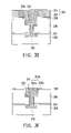
Referring to FIG. 1 , in order to prevent the corresponding metal layer 102 under the via opening from being damaged by etchant in the etching process of forming the trench, a recent method includes after a via opening 110 is formed in a dielectric layer 106, first filling a gap fill material 112 in the via opening 110 to prevent the corresponding metal layer 102 under the via opening 110 from being damaged by etchant. However, in the method, usually because of the shadowing effect of the gap fill material 112, after the trench 120 is formed in the subsequent etching, a dielectric layer 106 a with a fence shape is left at a corner 110 a of the via opening 110, thus causing the problem of the reliability of elements. However, it is quite difficult to eliminate the fence-shaped dielectric layer. It is applicable to adjust the height of the gap fill material to prevent the forming of the fence-shaped dielectric layer. However, under the influence of uniformity of etching and micro-loading effect, the thicknesses of the gap fill material at the center of the substrate and at the edge of the substrate, or the thicknesses of the gap fill material in a dense region and in a loose region of the substrate are greatly different, such that the process window is very narrow.
In another aspect, referring to FIG. 2 , in order to prevent the forming of the fence-shaped dielectric layer in the etching process, a polymer light process is adopted in a trench etching process. But, without the protection of the polymer, the dielectric layer 106 at the corner 120 a of the trench 120 is easily damaged by the etchant, and thus the corner 120 a of the trench 120 is rounded. After the metal layer 122 is deposited subsequently to fill in the trench with the rounded corner, the two neighboring dual damascene structures may be bridged subsequently.
Accordingly, the present invention is directed to provide a method of fabricating a dual damascene structure, in which the corner of a trench can be prevented from being rounded and also the bridging of two neighboring dual damascene structures can be overcome.
The present invention is also directed to provide a method of fabricating the dual damascene structure, in which the forming of a fence-shaped dielectric layer can be prevented.
The present invention is further directed to provide a method of forming a composite opening, in which the corner of a wide opening can be prevented from being rounded and the forming of a fence at the corner of the narrow opening can be prevented.
The present invention provides a dual damascene process. In the method, a dielectric layer is formed on the substrate in which a liner is formed, and a via opening is formed in the dielectric layer to expose the liner on the substrate. Then, a gap fill material is filled in the via opening, and a resistant layer is formed on the substrate. Next, a photolithographic process and an etching process are performed to form a trench in the dielectric layer to remain the gap fill material having a top surface with a convex shape. In the etching process, the etching rate of the gap fill material layer is larger than that of the resistant layer. Then, the gap fill material, the resistant layer, and the liner exposed by the via opening are removed, and a conductive layer is formed in the trench and the via opening.
In the dual damascene process according to an embodiment of the present invention, in the etching process, the etching selectivity of the gap fill material to the resistant layer ranges from 3 to 1.1.
In the dual damascene process according to an embodiment of the present invention, in the etching process, the etching rate of the gap fill material is larger than that of the dielectric layer.
In the dual damascene process according to an embodiment of the present invention, in the etching process, the etching selectivity of the gap fill material to the dielectric layer ranges from 1.2 to 2.
In the dual damascene process according to an embodiment of the present invention, the etching rate of the resistant layer is larger than that of the dielectric layer.
In the dual damascene process according to an embodiment of the present invention, in the etching process, an etching gas is free of oxygen.
In the dual damascene process according to an embodiment of the present invention, an etching gas used in the etching process includes fluorohydrocarbon.
In the dual damascene process according to an embodiment of the present invention, the etching gas further includes a carrier gas.
In the dual damascene process according to an embodiment of the present invention, the etching gas further includes an adjusted gas.
In the dual damascene process according to an embodiment of the present invention, the material of the dielectric layer comprises a low dielectric constant material.
According to the embodiment of the present invention, the dual damascene process further comprises forming a cap layer on the dielectric layer before the via opening is formed.
In the dual damascene process according to an embodiment of the present invention, the gap fill material comprises a polymer without anti-reflective property.
The present invention provides a method of forming a composite opening. A material layer is formed on a substrate, and then a narrow opening is formed in the material layer. Next, a gap fill material is formed in the narrow opening. After that, a resistant layer is formed on the substrate to cover the material layer and the gap fill material. Then, a photolithographic process and an etching process are performed to form a wide opening in communication with the narrow opening in the material layer, and to remain the gap fill material having a top surface with a convex shape, wherein in the etching process, the etching rate of the gap fill material larger than that of the resistant layer. Afterwards, the gap fill material and the resistant layer are removed to expose the wide opening and the narrow opening, so as to form the composite opening.
In the method of forming the composite opening according to an embodiment of the present invention, in the etching process, the etching selectivity of the gap fill material to the resistant layer ranges from 3 to 1.1.
In the method of forming the composite opening according to an embodiment of the present invention, in the etching process, the etching rate of the gap fill material is larger than that of the material layer.
In the method of forming the composite opening according to an embodiment of the present invention, in the etching process, the etching selectivity of the gap fill material to the material layer ranges from 1.2 to 2.
In the method of forming the composite opening according to an embodiment of the present invention, the etching rate of the resistant layer is larger than that of the material layer.
According to the embodiment of the present invention, in the method of forming the composite opening, the material of the gap fill material comprises a polymer without anti-reflective property.
According to the embodiment of the present invention, in the method of forming the composite opening, an etching gas used in the etching process includes fluorohydrocarbon.
According to the embodiment of the present invention, in the method of forming the composite opening, the etching gas further includes a carrier gas.
According to the embodiment of the present invention, in the method of forming the composite opening, the etching gas further includes an adjusted gas.
The method of fabricating the dual damascene structure of the present invention can prevent the corner of the trench from being rounded, prevent the two neighboring dual damascene structures from being bridged, and prevent the forming of the fence-shaped dielectric layer at the corner of the via opening.
The method of forming the composite opening of the present invention can prevent the corner of the wide opening from being rounded and prevent the corner of the narrow opening from forming the fence-shaped bump.
In order to the make aforementioned and other objects, features and advantages of the present invention comprehensible, preferred embodiments accompanied with figures are described in detail below.
Referring to FIG. 3A , the dual damascene structure of this embodiment is formed on a substrate 300. A conductive layer 302 is already formed on the substrate 300, and a liner 304 is already covered on the conductive layer 302. The substrate 300 is, for example, a semiconductor substrate, such as a silicon substrate or a silicon-on-insulator (SOI) substrate. The conductive layer 302 is, for example, a metal interconnect, such as a copper wire. The liner 304 covered on the conductive layer 302 can be used to prevent the conductive layer 302 from being oxidized, the material thereof is, for example, a layer of SiN, and the forming method is, for example, chemical vapor deposition (CVD). A dielectric layer 306 is formed on the liner 304, and the material thereof is, for example, a low dielectric constant material. The low dielectric constant material is a material layer with a dielectric constant lower than 4, for example fluorinated silicon glass (FSG); silsesquioxnane, such as hydrogen silsesquioxnane (HSQ), methyl silsesquioxane (MSQ), and hybrido-organo siloxane polymer (HOSP); aromatic hydrocarbon, such as SiLK; organosilicate glass, such as black diamond (BD), 3MS, 4MS; parylene; Fluoro-Polymer, such as PFCB, CYTOP, Teflon; poly(arylethers), such as PAE-2, FLARE; porous polymer, such as XLIK, Nanofoam, Awrogel; Coral; and the like. In an embodiment, a cap layer 308 is further formed on the dielectric layer 306, the material thereof is selected from a group consisting of silicon oxide (SiO), silicon nitride (SiN), silicon-oxy-nitride (SiON), silicon carbide (SiC), silicon oxycarbide (SiCO), silicon carbide nitride (SiCN), silicon carboxynitride (SiCNO) and the combination thereof and the forming method is, for example, CVD.
Then, referring to FIG. 3B , a photolithographic process and an etching process are performed, so as to form a via opening 310 in the dielectric layer 306. The etching gas used in the etching process is, for example, CF4/Ar/N2 or CHF3/Ar/N2. Then, a gap fill material 312 is filled in the via opening 310. The uniformity of the deposition of the gap fill material 312 is good, so the difference between the gap fill material 312 in the dense region and in the loose region is small. The material of the gap fill material 312 includes a polymer without anti-reflective property, for example, GF43 and DUV52, and the forming method is, for example, spin coating.
Afterwards, referring to FIG. 3C , a part of the gap fill material 312 is removed, and the gap fill material 312 a in the via opening 310 is left. The remaining gap fill material 312 a has a substantial flat surface or a depressed surface with lower central portion and higher sides. The process of removing a part of the gap fill material 312 can be an etch back process. Then, a resistant layer 314 such as a bottom anti-reflective coating is formed on the substrate 300. The height of the remaining gap fill material 312 a is not limited, and can be h1 or h2 (indicated by the dotted line). The uniformity of the etch back of the gap fill material 312 is good, and the difference between the remaining gap fill material 312 a in the dense region and in the loose region is not obvious. Therefore, the resistant layer 314 formed subsequently has a fine uniformity and the surface is quite flat. Also, in the subsequent photolithographic process, the quality of the patterning is not affected by the uneven height of the surface of the substrate. After that, a patterned photoresist layer 316 is formed on the resistant layer 314. The photoresist layer 316 has an opening pattern 318, and the opening pattern 318 is a pattern that is predetermined to form the trench in the dielectric layer 306.
Then, referring to FIG. 3D , the photoresist layer 316 is used as a mask to etch the resistant layer 314, the cap layer 308, and the dielectric layer 306, so as to transfer the opening pattern 318 to the dielectric layer 306 and to form a trench 320 in the dielectric layer 306. The trench 320 is communicated with the via opening 310. In the etching process, the etching rate of the gap fill material 312 a is larger than that of the resistant layer 314, and the etching rate of the gap fill material 312 a is larger than that of the dielectric layer 306. Preferably, the etching rate of the gap fill material 312 a is larger than that of the resistant layer 314, and the etching rate of the resistant layer 314 is larger than that of the dielectric layer 306. The etching selectivity of the gap fill material 312 a to the resistant layer 314 ranges, for example, from 3 to 1.1, and the etching selectivity of the gap fill material 312 a to the dielectric layer 306 ranges, for example, from 1.2 to 2. In an embodiment, in the etching process, an etching gas, for example, the gas free of oxygen, such as fluorohydrocarbon, which is capable of forming more polymers in the etching process is used as the etchant. The fluorohydrocarbon is selected from a group consisting of CF4, CF3H, CH2F2, CFH3, and the mixture thereof. In an embodiment, at 250 millitorr, CF4 of 155 sccm and CF3H of 95 seem are used as the etching gas to perform the etching process. In another embodiment, in the etching process, the etching gas further includes carrier gas such as argon in addition to fluorohydrocarbon. In another embodiment, in the etching process, the etching gas further includes an adjusted gas such as nitrogen and carbon monoxide in addition to fluorohydrocarbon and the carrier gas. As the etching gas used in the etching process is the etching gas that can form more polymers, and the polymer formed in the etching process can protect the dielectric layer at the corner of the trench from being damaged by etching. Therefore, the problem of bridging caused by the rounding of the corner of the trench will not occur. In another aspect, as the etching rate of the gap fill material 312 a is larger than that of the resistant layer 314 and the dielectric layer 306, in the etching process, the gap fill material 312 a when exposed is quickly etched, so that the gap fill material 312 b left after the etching process has a top surface with a convex shape. When the height of the gap fill material 312 a is high, i.e. h1, the remaining gap fill material 312 b is C1. When the height of the gap fill material 312 a is low, i.e. h2, the remaining gap fill material 312 b is C2 (indicated by the dotted line). No matter whether the gap fill material 312 b is C1 or C2, the shadowing effect of the gap fill material will not occur, and the fence-shaped dielectric layer will not be left at the corner of the via opening 310.
Then, referring to FIG. 3E , the photoresist layer 316, the resistant layer 314, and the gap fill material 312 b are removed. In an embodiment, the photoresist layer 316, the resistant layer 314, and the gap fill material 312 b can be removed at the same time through for example oxygen plasma ashing. Then, the liner 304 exposed by the via opening 310 is removed. Afterwards, a conductive layer 322 is formed on the substrate 300 and is filled in the trench 320 and the via opening 310. Usually, the conductive layer 322 includes a metal layer 324 and a barrier layer 326. The material of the barrier layer 326 is, for example, TiN or TaN. The metal layer 324 is, for example, a copper layer.
Then, referring to FIG. 3F , a part of the conductive layer 322 is removed, the conductive layer 322 a in the trench 320 and the via opening 310 is left. The conductive layer 322 a includes a metal layer 324 a and a barrier layer 326 a. The removing method can be chemical mechanical polishing. In the polishing process, the cap layer 308 is used as a polishing stop layer, so as to eliminate the problem of over-polishing the dielectric layer 306 due to the different polishing rates of the dense region and the loose region on the substrate 300.
Referring to FIG. 4A , a material layer 406 is formed on the substrate 400, the material thereof is not limited, and can be, for example, a dielectric layer such as a silicon oxide layer or any material that is predetermined to form the composite opening, and the forming method is, for example, CVD. Then, the photolithographic process and the etching process are performed to form a narrow opening 410 in the material layer 406. The etching gas used in the etching process is relative to the material of the dielectric layer. When the material layer 406 is silicon oxide, the etching gas is, for example, CF4/Ar/N2 or CHF3/Ar/N2. Then, a gap fill material 412 is filled in the narrow opening 410. The uniformity of the deposition of the gap fill material 412 is good, and the difference of the gap fill material 412 in the dense region and in the loose region is small. The material of the gap fill material 412 includes the polymer without anti-reflective property, for example, GF43 and DUV52, and the forming method is, for example, spin coating.
Then, referring to FIG. 4B , a part of the gap fill material 412 is removed, and the gap fill material 412 a in the narrow opening 410 is left. The remaining gap fill material 412 a has a substantial flat surface or a depressed surface with lower central portion and higher sides. The process of removing a part of the gap fill material 412 can be the etch back process. Then, a resistant layer 414 is formed on the substrate 400. The height of the remaining gap fill material 412 a is not limited and can be h3 or h4 (indicated by the dotted line). The uniformity of the etch back of the gap fill material 412 is good, and difference between the remaining gap fill material 412 a in the dense region and in the loose region is not obvious. Therefore, the resistant layer 414 formed subsequently has a fine uniformity and the surface is quite flat. In the subsequent photolithographic process, the quality of the patterning is not affected by the uneven height of the surface of the substrate. Afterwards, a patterned photoresist layer 416 is formed on the resistant layer 414. The photoresist layer 416 has an opening pattern 418, and the opening pattern 418 is a pattern that is predetermined to form the wide opening in the material layer 406.
Then, referring to FIG. 4C , the photoresist layer 416 is used as a mask to etch the resistant layer 414, and the material layer 406, so as to transfer the opening pattern 418 to the material layer 406 and to form a wide opening 420 in the material layer 406. The wide opening 420 is communicated with the narrow opening 410. In the etching process, the etching rate of the gap fill material 412 a is larger than that of the resistant layer 414, and the etching rate of the gap fill material 412 a is larger than that of the material layer 406. Preferably, the etching rate of the gap fill material 412 a is larger than that of the resistant layer 414, and the etching rate of the resistant layer 414 is larger than that of the material layer 406. The etching selectivity of the gap fill material 412 a to the resistant layer 414 ranges, for example, from 3 to 1.1, and the etching selectivity of the gap fill material 412 a to the material layer 406 ranges, for example, from 1.2 to 2. In an embodiment, the material layer 406 is silicon oxide. In the etching process, an etching gas, for example, the gas free of oxygen, such as fluorohydrocarbon, which is capable of forming more polymers in the etching process is used as the etchant. The fluorohydrocarbon is selected from a group consisting of CF4, CF3H, CH2F2, CFH3, and the mixture thereof. In an embodiment, at 250 millitorr, CF4 of 155 sccm and CF3H of 95 sccm are used as the etching gas to perform the etching process. In another embodiment, in the etching process, the etching gas further includes carrier gas such as argon in addition to fluorohydrocarbon. In another embodiment, in the etching process, the etching gas further includes an adjusted gas such as nitrogen and carbon monoxide in addition to fluorohydrocarbon and the carrier gas. As the etching gas used in the etching process is the etching gas that can form more polymers, and the polymer formed in the etching process can protect the dielectric layer at the corner of the wide opening from being damaged by etching. Therefore, the problem of rounding the corner of the wide opening will not occur. In another aspect, as the etching rate of the gap fill material 412 a is larger than that of the resistant layer 414 and the material layer 406, in the etching process, the gap fill material 412 a when exposed is quickly etched, so as to make the gap fill material 412 b left after the etching process has a top surface with a convex shape. When the height of the gap fill material 412 a is high, i.e. h3, the remaining gap fill material 412 b is C3. When the height of the gap fill material 412 a is low, i.e. h4, the remaining gap fill material 412 b is C4 (indicated by the dotted line). No matter whether the gap fill material 412 b is C3 or C4, the shadowing effect of the gap fill material will not occur, and the fence-shaped material layer is not left at the corner of the narrow opening 410.
Then, referring to FIG. 4D , the photoresist layer 416, the resistant layer 414, and the gap fill material 412 b are removed to expose the narrow opening 410, and the narrow opening 410 and the wide opening 420 constitute a composite opening 430. In an embodiment, the photoresist layer 416, the resistant layer 414, and the gap fill material 412 b can be removed at the same time through for example oxygen plasma ashing.
The method of fabricating the composite opening can be used in any process requiring that the wide opening and the narrow opening are formed at the same time.
The method of forming a composite opening of the present invention includes using a gap fill material with the etching rate larger than that of the resistant layer in the narrow opening first formed, and the remaining of the gap fill material having a top surface with a convex shape. Therefore, the present invention can prevent the corner of the wide opening from being rounded and prevent the forming of fence at the corner of the narrow opening.
The method of fabricating the dual damascene structure of the present invention is of using a gap fill material with the etching rate larger that of the resistant layer in the via opening first formed, and the remaining of the gap fill material having a top surface with a convex shape. Therefore, the present invention can prevent the corner of the trench from being rounded, operate an etching process in an oxygen-free atmosphere to prevent the two neighboring dual damascene structures from being bridged, and prevent the forming of the fence-shaped dielectric layer at the corner of the via opening.
It will be apparent to those skilled in the art that various modifications and variations can be made to the structure of the present invention without departing from the scope or spirit of the invention. In view of the foregoing, it is intended that the present invention modifications and variations of this invention provided they fall within the scope of the following claims and their equivalents.
Claims (21)
1. A dual damascene process, comprising:
providing a substrate, having a conductive region covered by a liner;
forming a dielectric layer on the liner;
forming a via opening in the dielectric layer to align with the conductive region and to expose the liner;
filling a gap fill material in the via opening;
forming a resistant layer on the substrate to cover the dielectric layer and the gap fill material;
performing a photolithographic process and an etching process to form a trench in the dielectric layer and to remain the gap fill material having a top surface with a convex shape, wherein in the etching process, the etching rate of the gap fill material is larger than that of the resistant layer
removing the gap fill material, the resistant layer, and the liner exposed by the via opening; and
forming a conductive layer in the trench and the via opening.
2. The dual damascene process as claimed in claim 1 , wherein in the etching process, the etching selectivity of the gap fill material to the resistant layer ranges from 3 to 1.1.
3. The dual damascene process as claimed in claim 1 , wherein in the etching process, the etching rate of the gap fill material is larger than that of the dielectric layer.
4. The dual damascene process as claimed in claim 3 , wherein in the etching process, the etching selectivity of the gap fill material to the dielectric layer ranges from 1.2 to 2.
5. The dual damascene process as claimed in claim 1 , wherein the etching rate of the resistant layer is larger than that of the dielectric layer.
6. The dual damascene process as claimed in claim 1 , wherein in the etching process, an etching gas is free of oxygen.
7. The dual damascene process as claimed in claim 1 , wherein an etching gas used in the etching process includes fluorohydrocarbon.
8. The dual damascene process as claimed in claim 7 , wherein the etching gas further includes a carrier gas.
9. The dual damascene process as claimed in claim 8 , wherein the etching gas further includes an adjusted gas.
10. The dual damascene process as claimed in claim 1 , wherein the material of the dielectric layer comprises a low dielectric constant material.
11. The dual damascene process as claimed in claim 1 , further comprising forming a cap layer on the dielectric layer before the via opening is formed.
12. The dual damascene process as claimed in claim 1 , wherein the gap fill layer comprises a polymer without anti-reflective property.
13. A method of forming a composite opening, comprising:
forming a material layer on a substrate;
forming a narrow opening in the material layer;
forming a gap fill material in the narrow opening;
forming a resistant layer on the substrate to cover the material layer and the gap fill material;
performing a photolithographic process and an etching process to form a wide opening in communication with the narrow opening in the material layer, and to remains the gap fill material having a top surface with a convex shape, wherein in the etching process, the etching rate of the gap fill material is larger than that of the resistant layer and
removing the gap fill material and the resistant layer to expose the wide opening and the narrow opening, so as to form the composite opening.
14. The method of forming the composite opening as claimed in claim 13 , wherein in the etching process, the etching selectivity of the gap fill material to the resistant layer ranges from 3 to 1.1.
15. The method of forming the composite opening as claimed in claim 13 , wherein in the etching process, the etching rate of the gap fill material is larger than that of the material layer.
16. The method of forming the composite opening as claimed in claim 15 , wherein in the etching process, the etching selectivity of the gap fill material to the material layer ranges from 1.2 to 2.
17. The method of forming the composite opening as claimed in claim 13 , wherein the etching rate of the resistant layer is larger than that of the material layer.
18. The method of forming the composite opening as claimed in claim 13 , wherein the material of the gap fill material comprises a polymer without anti-reflective property.
19. The method of forming the composite opening as claimed in claim 13 , wherein an etching gas used in the etching process includes fluorohydrocarbon.
20. The method of forming the composite opening as claimed in claim 19 , wherein the etching gas further includes a carrier gas.
21. The method of forming the composite opening as claimed in claim 20 , wherein the etching gas further includes an adjusted gas.
Priority Applications (2)
| Application Number | Priority Date | Filing Date | Title |
|---|---|---|---|
| US11/675,417 US7482266B2 (en) | 2007-02-15 | 2007-02-15 | Method of forming composite opening and method of dual damascene process using the same |
| SG200702455-7A SG145607A1 (en) | 2007-02-15 | 2007-04-03 | Method of forming composite opening and method of dual damascene process using the same |
Applications Claiming Priority (1)
| Application Number | Priority Date | Filing Date | Title |
|---|---|---|---|
| US11/675,417 US7482266B2 (en) | 2007-02-15 | 2007-02-15 | Method of forming composite opening and method of dual damascene process using the same |
Publications (2)
| Publication Number | Publication Date |
|---|---|
| US20080200025A1 US20080200025A1 (en) | 2008-08-21 |
| US7482266B2 true US7482266B2 (en) | 2009-01-27 |
Family
ID=39707050
Family Applications (1)
| Application Number | Title | Priority Date | Filing Date |
|---|---|---|---|
| US11/675,417 Active US7482266B2 (en) | 2007-02-15 | 2007-02-15 | Method of forming composite opening and method of dual damascene process using the same |
Country Status (2)
| Country | Link |
|---|---|
| US (1) | US7482266B2 (en) |
| SG (1) | SG145607A1 (en) |
Cited By (1)
| Publication number | Priority date | Publication date | Assignee | Title |
|---|---|---|---|---|
| US20140138830A1 (en) * | 2012-11-18 | 2014-05-22 | United Microelectronics Corp. | Metal interconnection structure |
Families Citing this family (1)
| Publication number | Priority date | Publication date | Assignee | Title |
|---|---|---|---|---|
| US11637068B2 (en) * | 2020-12-15 | 2023-04-25 | Globalfoundries U.S. Inc. | Thermally and electrically conductive interconnects |
Citations (5)
| Publication number | Priority date | Publication date | Assignee | Title |
|---|---|---|---|---|
| US6150252A (en) * | 1995-05-23 | 2000-11-21 | Texas Instruments Incorporated | Multi-stage semiconductor cavity filling process |
| US6472231B1 (en) * | 2001-01-29 | 2002-10-29 | Advanced Micro Devices, Inc. | Dielectric layer with treated top surface forming an etch stop layer and method of making the same |
| US20040077175A1 (en) * | 2002-10-21 | 2004-04-22 | Applied Materials, Inc. | Barc shaping for improved fabrication of dual damascene integrated circuit features |
| US20040147108A1 (en) * | 1999-08-26 | 2004-07-29 | Lamb James E. | Fill material for dual damascene processes |
| US20050085066A1 (en) * | 2003-10-16 | 2005-04-21 | Taiwan Semicondutor Manufacturing Co. | Novel method to reduce Rs pattern dependence effect |
-
2007
- 2007-02-15 US US11/675,417 patent/US7482266B2/en active Active
- 2007-04-03 SG SG200702455-7A patent/SG145607A1/en unknown
Patent Citations (5)
| Publication number | Priority date | Publication date | Assignee | Title |
|---|---|---|---|---|
| US6150252A (en) * | 1995-05-23 | 2000-11-21 | Texas Instruments Incorporated | Multi-stage semiconductor cavity filling process |
| US20040147108A1 (en) * | 1999-08-26 | 2004-07-29 | Lamb James E. | Fill material for dual damascene processes |
| US6472231B1 (en) * | 2001-01-29 | 2002-10-29 | Advanced Micro Devices, Inc. | Dielectric layer with treated top surface forming an etch stop layer and method of making the same |
| US20040077175A1 (en) * | 2002-10-21 | 2004-04-22 | Applied Materials, Inc. | Barc shaping for improved fabrication of dual damascene integrated circuit features |
| US20050085066A1 (en) * | 2003-10-16 | 2005-04-21 | Taiwan Semicondutor Manufacturing Co. | Novel method to reduce Rs pattern dependence effect |
Cited By (2)
| Publication number | Priority date | Publication date | Assignee | Title |
|---|---|---|---|---|
| US20140138830A1 (en) * | 2012-11-18 | 2014-05-22 | United Microelectronics Corp. | Metal interconnection structure |
| US8742587B1 (en) * | 2012-11-18 | 2014-06-03 | United Microelectronics Corp. | Metal interconnection structure |
Also Published As
| Publication number | Publication date |
|---|---|
| SG145607A1 (en) | 2008-09-29 |
| US20080200025A1 (en) | 2008-08-21 |
Similar Documents
| Publication | Publication Date | Title |
|---|---|---|
| CN100501969C (en) | Methods for forming interconnecting structure and semiconductor devices | |
| US9673087B2 (en) | Interconnect structures incorporating air-gap spacers | |
| US7326651B2 (en) | Method for forming damascene structure utilizing planarizing material coupled with compressive diffusion barrier material | |
| US7023093B2 (en) | Very low effective dielectric constant interconnect Structures and methods for fabricating the same | |
| US8080877B2 (en) | Damascene interconnection structure and dual damascene process thereof | |
| US20060148243A1 (en) | Method for fabricating a dual damascene and polymer removal | |
| US7323408B2 (en) | Metal barrier cap fabrication by polymer lift-off | |
| US7790601B1 (en) | Forming interconnects with air gaps | |
| US7015133B2 (en) | Dual damascene structure formed of low-k dielectric materials | |
| JP2006041519A (en) | Method of manufacturing dual damascene wiring | |
| JP2003045969A (en) | Wiring forming method utilizing dual damascene | |
| US7436009B2 (en) | Via structures and trench structures and dual damascene structures | |
| US7488687B2 (en) | Methods of forming electrical interconnect structures using polymer residues to increase etching selectivity through dielectric layers | |
| US7348277B2 (en) | Methods of fabricating semiconductor device using sacrificial layer | |
| US20070232062A1 (en) | Damascene interconnection having porous low k layer followed by a nonporous low k layer | |
| US7482266B2 (en) | Method of forming composite opening and method of dual damascene process using the same | |
| US20110097899A1 (en) | Method of forming funnel-shaped opening | |
| US20080057727A1 (en) | Method of manufacturing a semiconductor device | |
| US20070264843A1 (en) | Formation and applications of nitrogen-free silicon carbide in semiconductor manufacturing | |
| US20060099787A1 (en) | Method for damascene formation using plug materials having varied etching rates | |
| KR100753118B1 (en) | A forming method of contact hole | |
| KR20060075887A (en) | Method for forming metal-line of semiconductor device | |
| KR100606539B1 (en) | Method of fabricating metal layer of semiconductor device | |
| CN101261954A (en) | Forming method for compound open hole and dual metal inlay technology based on the method | |
| KR20050009426A (en) | Method for formating imd in semiconductor |
Legal Events
| Date | Code | Title | Description |
|---|---|---|---|
| AS | Assignment |
Owner name: UNITED MICROELECTRONICS CORP., TAIWAN Free format text: ASSIGNMENT OF ASSIGNORS INTEREST;ASSIGNOR:MA, HONG;REEL/FRAME:018910/0717 Effective date: 20070209 |
|
| STCF | Information on status: patent grant |
Free format text: PATENTED CASE |
|
| FPAY | Fee payment |
Year of fee payment: 4 |
|
| FPAY | Fee payment |
Year of fee payment: 8 |
|
| MAFP | Maintenance fee payment |
Free format text: PAYMENT OF MAINTENANCE FEE, 12TH YEAR, LARGE ENTITY (ORIGINAL EVENT CODE: M1553); ENTITY STATUS OF PATENT OWNER: LARGE ENTITY Year of fee payment: 12 |