US7471496B2 - Solenoid driving apparatus - Google Patents
Solenoid driving apparatus Download PDFInfo
- Publication number
- US7471496B2 US7471496B2 US11/265,181 US26518105A US7471496B2 US 7471496 B2 US7471496 B2 US 7471496B2 US 26518105 A US26518105 A US 26518105A US 7471496 B2 US7471496 B2 US 7471496B2
- Authority
- US
- United States
- Prior art keywords
- current
- switching element
- solenoid
- current switching
- circuit
- Prior art date
- Legal status (The legal status is an assumption and is not a legal conclusion. Google has not performed a legal analysis and makes no representation as to the accuracy of the status listed.)
- Expired - Fee Related
Links
- 239000004065 semiconductor Substances 0.000 description 7
- 238000001514 detection method Methods 0.000 description 6
- 230000007423 decrease Effects 0.000 description 3
- 230000003247 decreasing effect Effects 0.000 description 2
- 238000010586 diagram Methods 0.000 description 2
- 230000001939 inductive effect Effects 0.000 description 2
- 230000003071 parasitic effect Effects 0.000 description 2
- 239000000470 constituent Substances 0.000 description 1
- 238000010276 construction Methods 0.000 description 1
- 230000009189 diving Effects 0.000 description 1
- 230000020169 heat generation Effects 0.000 description 1
- 238000005259 measurement Methods 0.000 description 1
- 238000012986 modification Methods 0.000 description 1
- 230000004048 modification Effects 0.000 description 1
- 230000003252 repetitive effect Effects 0.000 description 1
- 239000000725 suspension Substances 0.000 description 1
Images


Classifications
-
- H—ELECTRICITY
- H01—ELECTRIC ELEMENTS
- H01H—ELECTRIC SWITCHES; RELAYS; SELECTORS; EMERGENCY PROTECTIVE DEVICES
- H01H47/00—Circuit arrangements not adapted to a particular application of the relay and designed to obtain desired operating characteristics or to provide energising current
- H01H47/22—Circuit arrangements not adapted to a particular application of the relay and designed to obtain desired operating characteristics or to provide energising current for supplying energising current for relay coil
- H01H47/32—Energising current supplied by semiconductor device
- H01H47/325—Energising current supplied by semiconductor device by switching regulator
-
- H—ELECTRICITY
- H02—GENERATION; CONVERSION OR DISTRIBUTION OF ELECTRIC POWER
- H02H—EMERGENCY PROTECTIVE CIRCUIT ARRANGEMENTS
- H02H9/00—Emergency protective circuit arrangements for limiting excess current or voltage without disconnection
- H02H9/04—Emergency protective circuit arrangements for limiting excess current or voltage without disconnection responsive to excess voltage
- H02H9/045—Emergency protective circuit arrangements for limiting excess current or voltage without disconnection responsive to excess voltage adapted to a particular application and not provided for elsewhere
- H02H9/047—Free-wheeling circuits
Definitions
- the present invention relates to a solenoid driving apparatus for driving a solenoid that is used, for example, for various controls of automobiles.
- a solenoid driving apparatus for driving a solenoid As a solenoid driving apparatus for driving a solenoid, a constant-current driving circuit for inductive loads has been known, which has semiconductor integrated circuits for driving inductive loads, as disclosed in Japanese Patent Application Laid-Open No. 2001-117651.
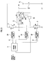
- FIG. 1 shows a typical circuit of a conventional solenoid driving apparatus.
- This solenoid driving apparatus includes a first current switching element 1 , a second current switching element 2 a, a third current switching element 3 , a battery E, a solenoid L, a resistor R, zener diodes ZD 1 and ZD 2 , a diode D 4 , an inverter 4 , and a control circuit 5 .
- the first current switching element 1 has a transistor Q 1 in the form of an N-channel MOSFET, and a diode D 1 connected between the source and drain of the transistor Q 1 .
- the second current switching element 2 a has a transistor Q 2 in the form of an N-channel MOSFET, and a diode D 2 connected between the source and drain of the transistor Q 2 .
- the third current switching element 3 has a transistor Q 3 in the form of an N-channel MOSFET, and a diode D 3 connected between the source and drain of the transistor Q 3 .
- Each of these diodes D 1 to D 3 is a parasitic diode.
- the drain of the transistor Q 1 is connected to the positive terminal of the battery E, and the negative terminal of the battery E is grounded.
- the source of the transistor Q 1 is connected to the source of the transistor Q 2 , and the gate of the transistor Q 1 is connected to the control circuit 5 .
- the drain of the transistor Q 2 is connected to the drain of the transistor Q 3 , and the gate of the transistor Q 2 is connected to the control circuit 5 .
- the source of the transistor Q 3 is grounded, and the gate of the transistor Q 3 is connected to the output end of the inverter 4 .
- the input end of the inverter 4 is connected to the control circuit 5 and the gate of the transistor Q 1 .
- One end of the solenoid L is connected to a junction A of the source of the transistor Q 1 and the source of the transistor Q 2 , and the other end of the solenoid L is grounded.
- a resistor R is connected between the gate and source of the transistor Q 2 .
- the gate of the transistor Q 2 is grounded through a series connection of a zener diode ZD 1 , a zener diode ZD 2 , and a diode D 4 .
- the solenoid driving apparatus when an exciting current is supplied from the battery E to the solenoid L, a control signal S 1 is fed from the control circuit 5 , and in response thereto, the first current switching element 1 is brought into a conductive state and the third current switching element 3 is brought into a non-conductive state. As a result, the flow of the exciting current into the second and the third current switching elements 2 a and 3 is blocked, and the exciting current is supplied to the solenoid L.
- the first current switching element 1 is brought into a non-conductive state and the third current switching element 3 is brought into a conductive state in response to the control signal S 1 , and at the same time, the second current switching element 2 a is brought into a conductive state in response to a control signal S 2 fed from the control circuit 5 .
- the first and the second current switching elements 1 and 2 a are brought into a non-conductive state and the third current switching element 3 is brought into a conductive state in response to the control signals Si and S 2 . Consequently, in the second current switching element 2 a , a constant-voltage operation is made by the zener diodes ZD 1 and ZD 2 as well as the diode D 4 . These are connected in series between the gate of the transistor Q 2 and the ground. The energy stored in the solenoid L is released in a short time by this constant-voltage operation.
- a high-accuracy resistor with a low resistance is generally used as a current detecting resistor.
- this resistor it is quite difficult to incorporate this resistor into a semiconductor chip because of constraints on area efficiency, current capacity, temperature characteristics, and the like. Therefore, when a current detecting circuit is formed in the semiconductor chip, a current detecting element is generally used which is connected in parallel to a current switching element and allows the passage of several hundredths or thousandths of a current passing through the current switching element.
- FIG. 2 shows the circuit of the conventional solenoid diving apparatus in which a current detecting circuit using current detecting elements is employed.
- the solenoid driving apparatus has the circuitry shown in FIG. 1 , and further includes a transistor Q 10 , a transistor Q 20 , a current detecting element r 1 , a current detecting element r 2 , a differential amplifier 10 , a differential amplifier 12 , and comparators 11 and 13 .
- the drain of the transistor Q 10 is connected to the drain of the transistor Q 1 , and the gate of the transistor Q 10 is connected to the gate of the transistor Q 1 .
- the source of the transistor Q 10 is connected to the source of the transistor Q 1 via the current detecting element r 1 .
- the drain of the transistor Q 20 is connected to the drain of the transistor Q 2 , the gate of the transistor Q 20 is connected to the gate of the transistor Q 2 , and the source of the transistor Q 20 is connected to the source of the transistor Q 2 via the current detecting element r 2 .
- Both ends of the current detecting element r 1 are connected to an inverting input terminal and a non-inverting input terminal of the differential amplifier 10 .
- the output end of the differential amplifier 10 is connected to a non-inverting input terminal of the comparator 11 .
- a reference voltage ref 1 is applied, and the output terminal of the comparator 11 is connected to the control circuit 5 .
- both ends of the current detecting element r 2 are connected an inverting input terminal and a non-inverting input terminal of the differential amplifier 12 .
- the output terminal of the differential amplifier 12 is connected to a non-inverting input terminal of the comparator 13 .
- a reference voltage ref 2 is applied to an inverting input terminal of the comparator 13 , and the output terminal of the comparator 13 is connected to the control circuit 5 .
- the control circuit 5 becomes operative in response to a control signal that is inputted externally, and generates and outputs a control signal S 1 for PWM control according to an output of the comparator 11 and an output of the comparator 13 .
- the current value of the exciting current supplied to the solenoid L is detected by the differential amplifier 10 as a voltage applied to the current detecting element r 1 connected to the source of the transistor Q 10 , and when this voltage is determined to reach or exceed the reference voltage ref 1 by the comparator 11 , this information is provided to the control circuit 5 .
- the current value of the loop current caused by the energy stored in the solenoid L is detected by the differential amplifier 12 as a voltage applied to the current detecting element r 2 connected to the source of the transistor Q 20 , and when this voltage is determined to fall down to or below the reference voltage ref 1 by the comparator 13 , this information is provided to the control circuit 5 .
- the control circuit 5 determines the pulse width of the control signal S 1 according to signals outputted from the comparators 11 and 13 .
- the conventional solenoid driving apparatus is configured so that the path used for supplying a current from the battery E to the solenoid L is provided independently of the path over which the loop current caused by the stored energy in the solenoid L passes therethrough as described above. Therefore, as shown in FIG. 2 , it is necessary to provide a current detecting circuit including the current detecting element r 1 , the differential amplifier 10 , and the comparator 11 , and another current detecting circuit including the current detecting element r 2 , the differential amplifier 12 , and the comparator 13 , in relation to the first current switching element 1 and the second current switching element 2 , respectively.
- the size of the current detecting circuit increases, and the amount of time and effort required for adjusting the constant-current value also increases. Furthermore, the measured current value contains errors in the two circuits, which disadvantageously does not lead to an improvement in current detection accuracy.
- the current passing through a solenoid can be controlled very accurately, and an inexpensive solenoid driving apparatus can be provided.
- a solenoid driving apparatus that drives a solenoid by intermittently supplying thereto an exciting current.
- the solenoid driving apparatus comprises: a first current switching element that opens and closes so as to switchably allow and block passage of the exciting current supplied to the solenoid; a loop current circuit that is connected to the first current switching element and passes a loop current caused by stored energy in the solenoid when the supply of the exciting current to the solenoid is stopped by the first current switching element; and a second current switching element that is disposed between the solenoid and a junction of the first current switching element and the loop current circuit, and opens and closes so as to switchably allow and block passage of the exciting current and the loop current.
- the loop current circuit includes a third current switching element that opens and closes exclusively against the first current switching element.
- the solenoid driving apparatus further comprises a control circuit that generates a control signal for controlling opening and closing of the second current switching element, and the second current switching element operates as a current switching element when the control signal is received from the control circuit and operates as a constant-voltage circuit when no control signal is received.
- the solenoid driving apparatus of the first or the second technical aspect comprises: a current detector that detects a value of a current passing through the second current switching element, and a control circuit that generates a control signal for controlling opening and closing of the first current switching element according to the current value detected by the current detector.
- FIG. 1 is an explanatory diagram of a conventional solenoid driving apparatus
- FIG. 2 is an explanatory diagram of another conventional solenoid driving apparatus
- FIG. 3 shows the circuit structure of a solenoid driving apparatus according to a first embodiment of the present invention
- FIG. 4 is a timing chart for explaining operations of the solenoid driving apparatus according to the first embodiment.
- FIG. 5 shows the circuit structure of a solenoid driving apparatus according to a second embodiment of the present invention.
- FIG. 3 shows a circuit structure of a solenoid driving apparatus according to a first embodiment of the present invention.
- the solenoid driving apparatus comprises a first current switching element 1 , a second current switching element 2 , a third current switching element 3 , a battery E, a solenoid L, a resistor R, a zener diode ZD 1 , a zener diode ZD 2 , a diode D 4 , an inverter 4 , a control circuit 5 , a transistor Q 20 , a current detecting element r 1 , a differential amplifier 10 , and gate drive circuits 20 , 21 , and 22 .
- a loop current circuit of the present invention corresponds to the third current switching element 3 .
- a current detector of the present invention comprises the transistor Q 20 , the current detecting element r 1 , and the differential amplifier 10 .
- the first current switching element 1 includes a transistor Q 1 in the form of an N-channel MOSFET, and a diode D 1 connected between the source and drain of the transistor Q 1 .
- the second current switching element 2 includes a transistor Q 2 in the form of an N-channel MOSFET, and a diode D 2 connected between the source and drain of the transistor Q 2 .
- the third current switching element 3 includes a transistor Q 3 in the form of an N-channel MOSFET, and a diode D 3 connected between the source and drain of the transistor Q 3 .
- Each of these diodes D 1 to D 3 is a parasitic diode.
- the drain of the transistor Q 1 is connected to the positive terminal of the battery E, and the negative terminal of the battery E is grounded.
- the source of the transistor Q 1 is connected to a junction A of the drain of the transistor Q 2 and the drain of the transistor Q 3 , and the gate of the transistor Q 1 is connected to the output end of the gate drive circuit 20 .
- the source of the transistor Q 2 is connected to one end of the solenoid L at a junction B, and the gate of the transistor Q 2 is connected to the output end of the gate drive circuit 21 .
- the other end of the solenoid L is grounded.
- the source of the transistor Q 3 is grounded, and the gate of the transistor Q 3 is connected to the output end of the gate drive circuit 22 .
- the gate drive circuit 20 generates a drive signal according to a control signal S 1 being outputted from the control circuit 5 , and sends the drive signal to the gate of the transistor Q 1 .
- the gate drive circuit 21 also generates a drive signal according to a control signal S 2 being outputted from the control circuit 5 , and sends the drive signal to the gate of the transistor Q 2 .
- the gate drive circuit 22 generates a drive signal according to a signal that is obtained by inverting the control signal S 1 being outputted from the control circuit 5 at the inverter 4 , and sends the drive signal to the gate of the transistor Q 3 .
- the resistor R is connected between the gate and source of the transistor Q 2 .
- the zener diode ZD 1 , the zener diode ZD 2 , and the diode D 4 are connected in series between the gate and drain of the transistor Q 2 .
- the drain of the transistor Q 20 is connected to the drain of the transistor Q 2 , the gate of the transistor Q 20 is connected to the gate of the transistor Q 2 , and the source of the transistor Q 20 is connected to the source of the transistor Q 2 via the current detecting element (impedance element) r 1 . Both ends of the current detecting element r 1 are connected to an inverting input terminal and a non-inverting input terminal of the differential amplifier 10 . The output terminal of the differential amplifier 10 is connected to the control circuit 5 .
- the control circuit 5 is activated in response to a control signal that is inputted externally.
- the control circuit 5 generates and outputs the control signal S 2 for turning the second current switching element 2 ON and OFF, and also generates and outputs the control signal S 1 for providing PWM control according to an output of the differential amplifier 10 .
- the control signal S 1 outputted from the control circuit 5 is fed to the gate of the first current switching element 1 via the gate drive circuit 20 , and is fed also to the gate of the third current switching element 3 via the gate drive circuit 22 after inverted by the inverter 4 . Therefore, the first current switching element 1 and the third current switching element 3 are turned ON and OFF in a mutually exclusive manner.
- the second current switching element 2 When the supply of the exciting current to the solenoid L is suspended, the second current switching element 2 remains in a conductive state according to the control signal S 2 , and the first current switching element 1 is brought into a non-conductive state and the third current switching element 3 is brought into a conductive state in response to the control signal S 1 . Therefore, the loop current caused by the energy stored in the solenoid L passes through the third current switching element 3 and the second current switching element 2 . This loop current gradually decreases with the slope determined by an inductance of the solenoid L.
- the magnitude of the exciting current and loop current passing through the second current switching element 2 are detected by a current detecting circuit which includes the transistor Q 20 , the current detecting element r 1 , and the differential amplifier 10 .
- a detection voltage corresponding to the current passing through the current detecting element r 1 is outputted by the differential amplifier 10 to the control circuit 5 .
- the control circuit 5 generates and outputs a control signal S 1 to stop the supply of the exciting current to the solenoid L when the detection voltage of the differential amplifier 10 (error voltage) increases to a first threshold value Vth 1 as shown in FIG. 4( c ).
- the loop current caused by the energy stored in the solenoid L starts to flow.
- the control circuit 5 stops the pass of the loop current when the detection voltage of the differential amplifier 10 decreases to a second threshold value Vth 2 as shown in FIG. 4( c ), and generates and outputs a control signal S 1 to turn on/off the first current switching element 1 .
- the exciting current of the solenoid L gradually increases again with the slope determined by an inductance of the solenoid L.
- the PWM control is performed by the intermittent on/off operations of the first and the third current switching elements 1 and 3 in response to the control signal S 1 , so that the constant-current control for the solenoid L is provided.
- the control signals S 1 and S 2 are fed from the control circuit 5 , and in response, the first and the second current switching elements 1 and 2 are brought into a non-conductive state.
- the second current switching element 2 makes a constant-voltage operation by use of the zener diodes ZD 1 and ZD 2 connected between the drain and gate of the second current switching element 2 .
- the second current switching element 2 is provided at the position where the path used for supplying the exciting current from the battery E to the solenoid L and the path through which the loop current passes due to the stored energy in the solenoid L overlap each other, so that the energy stored in the solenoid L can be released in a short time by the constant-voltage operation, and also the constant-current control can be provided with high accuracy.
- the number of the current detecting circuits of the present invention can be decreased to half, so that the size of the circuitry can be reduced. As a result, it becomes easy to form the solenoid driving apparatus within a semiconductor chip, and therefore an inexpensive solenoid driving apparatus can be provided.
- a solenoid driving apparatus according to a second embodiment of the present invention will be described below.
- the solenoid driving apparatus according to the second embodiment has the simplified configuration of the solenoid driving apparatus according to the first embodiment.
- FIG. 5 shows the circuit structure of the solenoid driving apparatus according to the second embodiment of the present invention.
- the solenoid driving apparatus is characterized such that a diode D 5 is employed instead of the third current switching element 3 which is used as the loop current circuit in the solenoid driving apparatus according to the first embodiment, and also a hysteresis comparator (Schmitt circuit) OP 1 is employed instead of the differential amplifier 10 in order to send an output of the hysteresis comparator OP 1 directly (bypassing the control circuit 5 ) to the gate drive circuit 20 .
- a diode D 5 is employed instead of the third current switching element 3 which is used as the loop current circuit in the solenoid driving apparatus according to the first embodiment
- a hysteresis comparator (Schmitt circuit) OP 1 is employed instead of the differential amplifier 10 in order to send an output of the hysteresis comparator OP 1 directly (bypassing the control circuit 5 ) to the gate drive circuit 20 .
- the exciting current When the exciting current is supplied to the solenoid L, the second current switching element 2 is brought into a conductive state in response to a control signal S 2 as shown in FIG. 4( b ) and the first current switching element 1 is in a conductive state according to a control signal S 1 being fed from the control circuit 5 as shown in FIG. 4( a ). Therefore, voltage is applied to the solenoid L as shown in FIG. 4( d ), and the exciting current is supplied from the battery E to the solenoid L through the first and the second current switching elements 1 and 2 . The exciting current gradually increases with the slope determined by an inductance of the solenoid L as shown in FIG. 4( c ).
- the output of the hysteresis comparator OP 1 indicates L-level which brings the first current switching element 1 into a non-conductive state.
- the solenoid L releases the stored energy by the loop current which gradually decreases with the slope determined by an inductance of the solenoid L.
- the output of the hysteresis comparator OP 1 is inverted and then indicates H-level which brings the first current switching element 1 into a conductive state.
- the above repetitive operations cause the first current switching element 1 to intermittently open and close, and the exciting current passing through the solenoid L is controlled in a current range determined by the first threshold value Vth 1 and the second threshold value Vth 2 .
- the solenoid driving apparatus in the second embodiment only ON/OFF operations of the second current switching element 2 in response to the control signal S 2 fed from the control circuit 5 can start and stop the constant-current control for the solenoid L. Furthermore, the diode 5 is employed for passing the loop current and also the hysteresys comparator OP 1 is employed to directly control the first current switching element 1 , and therefore the circuit of the solenoid driving apparatus is simplified and inexpensive.
- both an exciting current and a loop current pass through the second current switching element, so that the number of current detecting circuits for measuring these exciting current and loop current is reduced to half of the conventional count.
- the loop current circuit comprises the third current switching element that turns ON and OFF exclusively with respect to the first current switching element, so that losses caused by the loop current can be reduced more compared to, for example, the case where a diode is used as loop current circuit.
- heat generation is suppressed in a solenoid driving apparatus formed of semiconductors, thereby leading to a miniaturized semiconductor package.
- the second current switching element operates as a current switching element when a control signal for turning on/off thereof is received, and is also operates as a constant-voltage circuit when no control signal is received. Therefore, the energy stored in the solenoid can be released in a short time when the second current switching element operates as the constant-voltage circuit.
- the value of a current passing through the second current switching element is detected, and a control signal is generated based on this detected current value, so that constant-current control can be provided with high accuracy. Furthermore, the number of current detection circuits can be decreased to half compared to a solenoid driving apparatus to which the conventional current detecting circuits are applied, so that the size of the circuitry can be reduced. As a result, it becomes easy to form a solenoid driving apparatus within a semiconductor chip, and therefore an inexpensive solenoid driving apparatus can be provided.
- the present invention is applicable to a solenoid driving apparatus for driving a solenoid used for various controls of automobiles and the like.
Landscapes
- Engineering & Computer Science (AREA)
- Power Engineering (AREA)
- Electronic Switches (AREA)
Abstract
Description
Claims (9)
Applications Claiming Priority (2)
| Application Number | Priority Date | Filing Date | Title |
|---|---|---|---|
| JP2004-325103 | 2004-11-09 | ||
| JP2004325103A JP4561321B2 (en) | 2004-11-09 | 2004-11-09 | Solenoid drive |
Publications (2)
| Publication Number | Publication Date |
|---|---|
| US20060098376A1 US20060098376A1 (en) | 2006-05-11 |
| US7471496B2 true US7471496B2 (en) | 2008-12-30 |
Family
ID=36316078
Family Applications (1)
| Application Number | Title | Priority Date | Filing Date |
|---|---|---|---|
| US11/265,181 Expired - Fee Related US7471496B2 (en) | 2004-11-09 | 2005-11-03 | Solenoid driving apparatus |
Country Status (3)
| Country | Link |
|---|---|
| US (1) | US7471496B2 (en) |
| JP (1) | JP4561321B2 (en) |
| DE (1) | DE102005053472A1 (en) |
Families Citing this family (5)
| Publication number | Priority date | Publication date | Assignee | Title |
|---|---|---|---|---|
| JP2008028083A (en) * | 2006-07-20 | 2008-02-07 | Shindengen Mechatronics Co Ltd | Solenoid drive control circuit, and solenoid |
| EP2872098B1 (en) * | 2012-07-10 | 2019-03-20 | Koninklijke Philips N.V. | A device for treating skin |
| DE102012107953B3 (en) * | 2012-08-29 | 2014-02-13 | Sma Solar Technology Ag | Circuit arrangement for driving a bistable relay |
| JP7459578B2 (en) * | 2020-03-16 | 2024-04-02 | 株式会社アイシン | Solenoid valve drive circuit |
| US11488798B2 (en) * | 2020-03-17 | 2022-11-01 | Hamilton Sundstrand Corporation | Current source contactor drive with economizers |
Citations (10)
| Publication number | Priority date | Publication date | Assignee | Title |
|---|---|---|---|---|
| JPS5448150A (en) * | 1977-09-26 | 1979-04-16 | Hitachi Ltd | Curernt switch circuit |
| US5267545A (en) * | 1989-05-19 | 1993-12-07 | Orbital Engine Company (Australia) Pty. Limited | Method and apparatus for controlling the operation of a solenoid |
| US5469825A (en) * | 1994-09-19 | 1995-11-28 | Chrysler Corporation | Fuel injector failure detection circuit |
| US5914849A (en) * | 1994-04-26 | 1999-06-22 | Kilovac Corporation | DC actuator control circuit with voltage compensation, current control and fast dropout period |
| US6078204A (en) * | 1996-12-19 | 2000-06-20 | Texas Instruments Incorporated | High current drain-to-gate clamp/gate-to-source clamp for external power MOS transistors |
| US6216678B1 (en) * | 2000-01-19 | 2001-04-17 | Ford Global Technologies, Inc. | Method and apparatus for generating and identifying misfires |
| JP2001117651A (en) | 1999-10-15 | 2001-04-27 | Mitsubishi Electric Corp | Inductive load constant current drive circuit |
| US20020104494A1 (en) * | 2001-02-07 | 2002-08-08 | Honda Giken Kogyo Kabushiki Kaisha | Controller for controlling an electromagnetic actuator |
| US6584961B2 (en) * | 2000-08-04 | 2003-07-01 | Magneti Marelli Powertrain S.P.A. | Method and device for driving an injector in an internal combustion engine |
| US6721158B2 (en) * | 1999-12-24 | 2004-04-13 | Conti Temic Microelectronic Gmbh | Method for providing current by means of an inductive component |
Family Cites Families (7)
| Publication number | Priority date | Publication date | Assignee | Title |
|---|---|---|---|---|
| JP2536949B2 (en) * | 1990-04-26 | 1996-09-25 | 株式会社小松製作所 | Inductance load drive circuit |
| JPH0446231U (en) * | 1990-08-24 | 1992-04-20 | ||
| JPH04354106A (en) * | 1991-05-31 | 1992-12-08 | Hitachi Ltd | Solenoid driving circuit and car-mounted at control equipment |
| JP2815744B2 (en) * | 1991-12-25 | 1998-10-27 | 三菱電機株式会社 | Integrated circuit for driving inductive load constant current |
| JP2000058320A (en) * | 1998-08-05 | 2000-02-25 | Zexel Corp | Solenoid drive circuit |
| JP4055882B2 (en) * | 2000-08-31 | 2008-03-05 | 株式会社小松製作所 | Solenoid drive |
| JP2002319506A (en) * | 2001-04-20 | 2002-10-31 | Sanken Electric Co Ltd | Solenoid drive device |
-
2004
- 2004-11-09 JP JP2004325103A patent/JP4561321B2/en not_active Expired - Fee Related
-
2005
- 2005-11-03 US US11/265,181 patent/US7471496B2/en not_active Expired - Fee Related
- 2005-11-09 DE DE102005053472A patent/DE102005053472A1/en not_active Withdrawn
Patent Citations (10)
| Publication number | Priority date | Publication date | Assignee | Title |
|---|---|---|---|---|
| JPS5448150A (en) * | 1977-09-26 | 1979-04-16 | Hitachi Ltd | Curernt switch circuit |
| US5267545A (en) * | 1989-05-19 | 1993-12-07 | Orbital Engine Company (Australia) Pty. Limited | Method and apparatus for controlling the operation of a solenoid |
| US5914849A (en) * | 1994-04-26 | 1999-06-22 | Kilovac Corporation | DC actuator control circuit with voltage compensation, current control and fast dropout period |
| US5469825A (en) * | 1994-09-19 | 1995-11-28 | Chrysler Corporation | Fuel injector failure detection circuit |
| US6078204A (en) * | 1996-12-19 | 2000-06-20 | Texas Instruments Incorporated | High current drain-to-gate clamp/gate-to-source clamp for external power MOS transistors |
| JP2001117651A (en) | 1999-10-15 | 2001-04-27 | Mitsubishi Electric Corp | Inductive load constant current drive circuit |
| US6721158B2 (en) * | 1999-12-24 | 2004-04-13 | Conti Temic Microelectronic Gmbh | Method for providing current by means of an inductive component |
| US6216678B1 (en) * | 2000-01-19 | 2001-04-17 | Ford Global Technologies, Inc. | Method and apparatus for generating and identifying misfires |
| US6584961B2 (en) * | 2000-08-04 | 2003-07-01 | Magneti Marelli Powertrain S.P.A. | Method and device for driving an injector in an internal combustion engine |
| US20020104494A1 (en) * | 2001-02-07 | 2002-08-08 | Honda Giken Kogyo Kabushiki Kaisha | Controller for controlling an electromagnetic actuator |
Also Published As
| Publication number | Publication date |
|---|---|
| JP2006135242A (en) | 2006-05-25 |
| JP4561321B2 (en) | 2010-10-13 |
| DE102005053472A1 (en) | 2006-06-08 |
| US20060098376A1 (en) | 2006-05-11 |
Similar Documents
| Publication | Publication Date | Title |
|---|---|---|
| US7336085B2 (en) | Current sensing circuit | |
| US9231472B2 (en) | System and method for a switched-mode power supply | |
| US7166993B2 (en) | Step-down switching regulator | |
| JP5526185B2 (en) | Battery charger with common control loop for low dropout voltage regulator and boost regulator | |
| US20050013079A1 (en) | Power supply control apparatus including highly-reliable overcurrent detecting circuit | |
| CN102237798B (en) | Apparatus and method for detecting changes in output voltage of an isolated power converter | |
| US5192906A (en) | Switching regulator with current limiting shutdown | |
| US8040116B2 (en) | Automatically configurable dual regulator type circuits and methods | |
| US7576526B2 (en) | Overcurrent detection circuit | |
| US6785106B2 (en) | Integrate circuit device | |
| JP4630764B2 (en) | Method and apparatus for sensing positive and negative peak inductor current without loss in a high side switch | |
| US10942536B1 (en) | Pre-regulator for an LDO | |
| CN101197534B (en) | Dc/dc converter | |
| CN101820221B (en) | toggle regulator | |
| KR101856694B1 (en) | An Apparatus And A Method For Testing A Low-side Driving IC | |
| US11632033B2 (en) | Switching control circuit and power supply circuit | |
| CN100422751C (en) | Undercurrent sensing apparatus and method | |
| US20060209481A1 (en) | Switching mode power supply and method for performing protection operation thereof | |
| US11936302B2 (en) | Detection circuit, switching control circuit, and power supply circuit | |
| US7471496B2 (en) | Solenoid driving apparatus | |
| US5986441A (en) | Circuit configuration for capturing the load current of a power semiconductor component with a load on the source side | |
| US11616445B2 (en) | Method for driving a switch in a power converter, drive circuit and power converter | |
| US20080197910A1 (en) | Input processing circuit and switch input circuit using the same | |
| US10333452B2 (en) | Control apparatus and method for sensing overcurrent of DC motor of vehicle | |
| US20040164787A1 (en) | Circuit arrangement and method for actuating a semiconductor switch connected in series with an inductive load |
Legal Events
| Date | Code | Title | Description |
|---|---|---|---|
| AS | Assignment |
Owner name: SANKEN ELECTRIC CO., LTD., JAPAN Free format text: ASSIGNMENT OF ASSIGNORS INTEREST;ASSIGNORS:SATOH, KIYOKATSU;KATOH, JUNICHI;REEL/FRAME:017189/0987 Effective date: 20051027 |
|
| STCF | Information on status: patent grant |
Free format text: PATENTED CASE |
|
| FPAY | Fee payment |
Year of fee payment: 4 |
|
| FEPP | Fee payment procedure |
Free format text: PAYOR NUMBER ASSIGNED (ORIGINAL EVENT CODE: ASPN); ENTITY STATUS OF PATENT OWNER: LARGE ENTITY |
|
| FPAY | Fee payment |
Year of fee payment: 8 |
|
| FEPP | Fee payment procedure |
Free format text: MAINTENANCE FEE REMINDER MAILED (ORIGINAL EVENT CODE: REM.); ENTITY STATUS OF PATENT OWNER: LARGE ENTITY |
|
| LAPS | Lapse for failure to pay maintenance fees |
Free format text: PATENT EXPIRED FOR FAILURE TO PAY MAINTENANCE FEES (ORIGINAL EVENT CODE: EXP.); ENTITY STATUS OF PATENT OWNER: LARGE ENTITY |
|
| STCH | Information on status: patent discontinuation |
Free format text: PATENT EXPIRED DUE TO NONPAYMENT OF MAINTENANCE FEES UNDER 37 CFR 1.362 |
|
| FP | Lapsed due to failure to pay maintenance fee |
Effective date: 20201230 |