JP5526185B2 - Battery charger with common control loop for low dropout voltage regulator and boost regulator - Google Patents
Battery charger with common control loop for low dropout voltage regulator and boost regulator Download PDFInfo
- Publication number
- JP5526185B2 JP5526185B2 JP2012105205A JP2012105205A JP5526185B2 JP 5526185 B2 JP5526185 B2 JP 5526185B2 JP 2012105205 A JP2012105205 A JP 2012105205A JP 2012105205 A JP2012105205 A JP 2012105205A JP 5526185 B2 JP5526185 B2 JP 5526185B2
- Authority
- JP
- Japan
- Prior art keywords
- current
- charging
- battery
- voltage
- circuit
- Prior art date
- Legal status (The legal status is an assumption and is not a legal conclusion. Google has not performed a legal analysis and makes no representation as to the accuracy of the status listed.)
- Active
Links
- 230000009977 dual effect Effects 0.000 claims description 31
- 238000000034 method Methods 0.000 claims description 9
- 238000001514 detection method Methods 0.000 claims description 8
- 238000004891 communication Methods 0.000 claims description 4
- 238000010586 diagram Methods 0.000 description 8
- 230000007704 transition Effects 0.000 description 6
- 230000007423 decrease Effects 0.000 description 4
- 238000012986 modification Methods 0.000 description 2
- 230000004048 modification Effects 0.000 description 2
- 238000012544 monitoring process Methods 0.000 description 2
- 230000008569 process Effects 0.000 description 2
- 230000008859 change Effects 0.000 description 1
- 238000011161 development Methods 0.000 description 1
- 238000004146 energy storage Methods 0.000 description 1
- 239000000463 material Substances 0.000 description 1
- 230000000135 prohibitive effect Effects 0.000 description 1
- 239000004065 semiconductor Substances 0.000 description 1
- 230000001960 triggered effect Effects 0.000 description 1
Images


Classifications
-
- H—ELECTRICITY
- H02—GENERATION; CONVERSION OR DISTRIBUTION OF ELECTRIC POWER
- H02J—CIRCUIT ARRANGEMENTS OR SYSTEMS FOR SUPPLYING OR DISTRIBUTING ELECTRIC POWER; SYSTEMS FOR STORING ELECTRIC ENERGY
- H02J7/00—Circuit arrangements for charging or depolarising batteries or for supplying loads from batteries
- H02J7/02—Circuit arrangements for charging or depolarising batteries or for supplying loads from batteries for charging batteries from ac mains by converters
- H02J7/04—Regulation of charging current or voltage
-
- H—ELECTRICITY
- H02—GENERATION; CONVERSION OR DISTRIBUTION OF ELECTRIC POWER
- H02J—CIRCUIT ARRANGEMENTS OR SYSTEMS FOR SUPPLYING OR DISTRIBUTING ELECTRIC POWER; SYSTEMS FOR STORING ELECTRIC ENERGY
- H02J7/00—Circuit arrangements for charging or depolarising batteries or for supplying loads from batteries
- H02J7/007—Regulation of charging or discharging current or voltage
- H02J7/0071—Regulation of charging or discharging current or voltage with a programmable schedule
-
- H—ELECTRICITY
- H01—ELECTRIC ELEMENTS
- H01M—PROCESSES OR MEANS, e.g. BATTERIES, FOR THE DIRECT CONVERSION OF CHEMICAL ENERGY INTO ELECTRICAL ENERGY
- H01M10/00—Secondary cells; Manufacture thereof
- H01M10/42—Methods or arrangements for servicing or maintenance of secondary cells or secondary half-cells
- H01M10/46—Accumulators structurally combined with charging apparatus
-
- H—ELECTRICITY
- H02—GENERATION; CONVERSION OR DISTRIBUTION OF ELECTRIC POWER
- H02J—CIRCUIT ARRANGEMENTS OR SYSTEMS FOR SUPPLYING OR DISTRIBUTING ELECTRIC POWER; SYSTEMS FOR STORING ELECTRIC ENERGY
- H02J7/00—Circuit arrangements for charging or depolarising batteries or for supplying loads from batteries
- H02J7/007—Regulation of charging or discharging current or voltage
- H02J7/00712—Regulation of charging or discharging current or voltage the cycle being controlled or terminated in response to electric parameters
- H02J7/007182—Regulation of charging or discharging current or voltage the cycle being controlled or terminated in response to electric parameters in response to battery voltage
-
- Y—GENERAL TAGGING OF NEW TECHNOLOGICAL DEVELOPMENTS; GENERAL TAGGING OF CROSS-SECTIONAL TECHNOLOGIES SPANNING OVER SEVERAL SECTIONS OF THE IPC; TECHNICAL SUBJECTS COVERED BY FORMER USPC CROSS-REFERENCE ART COLLECTIONS [XRACs] AND DIGESTS
- Y02—TECHNOLOGIES OR APPLICATIONS FOR MITIGATION OR ADAPTATION AGAINST CLIMATE CHANGE
- Y02E—REDUCTION OF GREENHOUSE GAS [GHG] EMISSIONS, RELATED TO ENERGY GENERATION, TRANSMISSION OR DISTRIBUTION
- Y02E60/00—Enabling technologies; Technologies with a potential or indirect contribution to GHG emissions mitigation
- Y02E60/10—Energy storage using batteries
Landscapes
- Engineering & Computer Science (AREA)
- Power Engineering (AREA)
- Manufacturing & Machinery (AREA)
- Chemical & Material Sciences (AREA)
- Chemical Kinetics & Catalysis (AREA)
- Electrochemistry (AREA)
- General Chemical & Material Sciences (AREA)
- Charge And Discharge Circuits For Batteries Or The Like (AREA)
- Secondary Cells (AREA)
Description
本発明はバッテリ充電装置に関し、具体的には、二つの異なる充電モードの間でスムースな移行を提供するバッテリ充電装置に関する。 The present invention relates to battery charging devices, and more particularly to battery charging devices that provide a smooth transition between two different charging modes.
現在、より高い性能の電源回路の必要性が増加しており、これが電圧レギュレータ・デバイスの進展をもたらした。例えば、携帯電話、ページャ、ラップトップ、カメラ・レコーダおよびその他のモバイル・バッテリで動作する機器で使用する場合のように、多くの低電圧応用製品では、低ドロップアウト(LDO)電圧レギュレータを使用することが要求される。 Currently, there is an increasing need for higher performance power circuits, which has led to the development of voltage regulator devices. Many low-voltage applications use low dropout (LDO) voltage regulators, such as when used in mobile phones, pagers, laptops, camera recorders, and other mobile battery-powered devices. Is required.
一般的に、LDO電圧レギュレータは、その入力と出力の電圧差が低く、きちんと規定され、安定したDC電圧を供給することができる。通常、電気回路に所要電力を与えるため、LDO電圧レギュレータを構成する。LDO電圧レギュレータは、典型的には、誤差増幅器と、例えば電力トランジスタのようなパス・デバイスとを持つ。これら二つの構成部品は直列に接続される。誤差増幅器はLDO電圧レギュレータの入力端子に接続され、パス・デバイスはLDO電圧レギュレータの出力端子に接続される。その結果、パス・デバイスは外部負荷を駆動することができる。しかしながら、LDO電圧レギュレータは、充電されるバッテリの電圧が増加するとその効率を失い、LDO電圧レギュレータでの入力−出力電圧差が低下する。 Generally, an LDO voltage regulator has a low voltage difference between its input and output, is well defined, and can supply a stable DC voltage. Normally, an LDO voltage regulator is configured to provide the required power to the electrical circuit. An LDO voltage regulator typically has an error amplifier and a pass device such as a power transistor. These two components are connected in series. The error amplifier is connected to the input terminal of the LDO voltage regulator, and the pass device is connected to the output terminal of the LDO voltage regulator. As a result, the pass device can drive an external load. However, the LDO voltage regulator loses its efficiency when the voltage of the battery to be charged increases, and the input-output voltage difference at the LDO voltage regulator decreases.
電子デバイスにDC電流を供給するために一般的に使用するもう一つのレギュレータはブースト・レギュレータである。それは、少なくとも2個の半導体スイッチと少なくとも1個のエネルギー蓄積素子とを含むスイッチィング・モード電源回路の類である。ブースト・レギュレータは、その入力DC電圧より高い出力DC電圧を供給することができ、充電されるバッテリの電圧がより高い場合、バッテリ充電動作に特に便利である。 Another regulator commonly used to supply DC current to electronic devices is a boost regulator. It is a type of switching mode power supply circuit that includes at least two semiconductor switches and at least one energy storage element. A boost regulator can provide an output DC voltage that is higher than its input DC voltage, and is particularly useful for battery charging operations when the voltage of the battery being charged is higher.
LDO電圧レギュレータとブースト・レギュレータとの性質を組み合わせ、これらの二つの形式のレギュレータ間の同時スムース切替動作で、入力電圧より高い出力電圧を供給できるようなバッテリ充電デバイスを持つことは、望ましいことである。 It would be desirable to have a battery charging device that combines the properties of an LDO voltage regulator and a boost regulator to provide an output voltage higher than the input voltage with simultaneous smooth switching operation between these two types of regulators. is there.
一つの実施形態では、本発明は、二つの異なるモードでバッテリを充電し、充電電流を殆ど一定に保持しながら二つのモード間を移行するという、デュアル・モード充電器である。デュアル・モード充電器には、制御回路、ブースト回路および低ドロップアウト回路を含む。ブースト回路は制御回路と通信し、入力ソースから入力電流を受信する。ブースト回路は、デュアル・モード充電器がブースト・モードで動作できるようにする。低ドロップアウト回路は制御回路およびブースト回路と通信する。低ドロップアウト回路はバッテリに充電電流を出力し、デュアル・モード充電器が低ドロップアウト・モードで動作できるようにする。制御回路は入力電流と充電電流とを監視し、ブースト回路と低ドロップアウト回路とを同時に制御する。また、制御回路は、デュアル・モード充電器が低ドロップアウト・モードからブースト・モードに切替える間、充電電流を一定に保持する。 In one embodiment, the present invention is a dual mode charger that charges the battery in two different modes and transitions between the two modes while keeping the charging current almost constant. The dual mode charger includes a control circuit, a boost circuit and a low dropout circuit. The boost circuit communicates with the control circuit and receives input current from the input source. The boost circuit allows the dual mode charger to operate in boost mode. The low dropout circuit communicates with the control circuit and the boost circuit. The low dropout circuit outputs charge current to the battery, allowing the dual mode charger to operate in low dropout mode. The control circuit monitors the input current and the charging current, and controls the boost circuit and the low dropout circuit simultaneously. The control circuit also keeps the charging current constant while the dual mode charger switches from the low dropout mode to the boost mode.
もう一つの実施形態では、本発明は、制御回路と、制御回路と通信するブースト回路と、制御回路およびブースト回路と通信する低ドロップアウト回路とを備えるデュアル・モード充電器である。低ドロップアウト回路はバッテリに充電電流を出力する。制御回路はブースト回路と低ドロップアウト回路とを同時に制御する。デュアル・モード充電器は、充電電流を一定に保持しながらブースト回路と低ドロップアウト回路との間で充電動作を切替える。 In another embodiment, the present invention is a dual mode charger comprising a control circuit, a boost circuit in communication with the control circuit, and a low dropout circuit in communication with the control circuit and the boost circuit. The low dropout circuit outputs charging current to the battery. The control circuit controls the boost circuit and the low dropout circuit simultaneously. The dual mode charger switches the charging operation between the boost circuit and the low dropout circuit while keeping the charging current constant.
更にもう一つの実施形態では、本発明はデュアル・モード充電器を使用してバッテリを充電する方法である。本方法には、デュアル・モード充電器を低ドロップアウト・モードで動作可能にすることと、バッテリに充電電流を出力することと、バッテリの電圧を充電アダプタの電圧と比較することと、もしバッテリの電圧が充電アダプタの電圧とほぼ等しい場合、充電電流を一定に保持しながら低ドロップアウト・モードからブースト・モードにデュアル・モード充電器を切替えることとを備える。 In yet another embodiment, the present invention is a method of charging a battery using a dual mode charger. The method includes enabling a dual mode charger to operate in a low dropout mode, outputting charge current to the battery, comparing the battery voltage to the voltage of the charge adapter, and Switching the dual mode charger from the low dropout mode to the boost mode while keeping the charging current constant.
本発明の利点は、それらの典型的な実施形態についての以下の詳細な説明から明らかになるであろうが、その説明は、次の添付の図面に関連して考察される。 The advantages of the present invention will become apparent from the following detailed description of these exemplary embodiments, which description is considered in conjunction with the following accompanying drawings.
要求に応じて、本発明の詳細な実施形態について本明細書で開示する。理解されなければならないことであるが、開示する実施形態は、色々の別の形式およびそれらの組合せで実装できる可能性のある本開示の単なる典型的な例である。本明細書で使用するように、単語“典型的な”は、説明、見本、モデルおよびパターンとして役に立つ実施形態を参照するために、拡張して使用される。図は必ずしも拡大縮小される必要はなく、幾つかの特徴は、特別な構成部品の詳細を示すため、誇張されたり、または最小にされたりする可能性がある。他の事例では、周知の構成部品、システム、材料または方法については、本開示を曖昧にすることをさけるため、詳細に説明されていない。従って、本明細書で開示する特定の構造的および機能的詳細は、制限するものとしてではなく、単に、本特許請求範囲のための基礎として、また、当開示を様々に採用するため当事業者に教示する代表的な基礎として、解釈されるべきである。 As required, detailed embodiments of the present invention are disclosed herein. It should be understood that the disclosed embodiments are merely exemplary of the present disclosure that could be implemented in a variety of other forms and combinations thereof. As used herein, the word “typical” is used extensively to refer to embodiments that serve as descriptions, samples, models, and patterns. The figures do not necessarily have to be scaled, and some features may be exaggerated or minimized to show details of particular components. In other instances, well-known components, systems, materials or methods have not been described in detail in order to avoid obscuring the present disclosure. Accordingly, the specific structural and functional details disclosed herein are not intended to be limiting, but merely as a basis for the claims and to employ the disclosure variously. Should be interpreted as a representative basis to teach.
本発明は、バッテリの電圧レベルに依存して、二つの異なるモードでバッテリを充電する、柔軟なデュアル・モード・バッテリ充電器を提供し、これらの二つのモード間でスムースな移行を行い、前記移行の間、充電電流は比較的一定に保持されている。より低いバッテリ・レベルでは、デュアル・モード・バッテリ充電器はLDO充電器としてバッテリを充電し、バッテリ電圧がアダプタ電圧に非常に近い場合は、前記充電器はその動作モードをLDOモードからブースト・モードに移行し、ブースト充電器としてバッテリを充電する。一つはLDO充電器のため、一つはブースト充電器のためというように二つの独立した制御回路を使用する代わりに、この柔軟なバッテリ充電器は、LDO充電器とブースト充電器との動作を制御するため一つの共通の制御回路を使用する。共通制御回路のため、一つの動作モードから他の動作モードへの切替動作はスムースで緩やかである。切替動作は自動的であり、アダプタ電圧とバッテリ電圧間の差でトリガされる。 The present invention provides a flexible dual-mode battery charger that charges the battery in two different modes depending on the voltage level of the battery, provides a smooth transition between these two modes, and During the transition, the charging current is kept relatively constant. At lower battery levels, the dual mode battery charger will charge the battery as an LDO charger, and if the battery voltage is very close to the adapter voltage, the charger will change its operating mode from LDO mode to boost mode. Go to and charge the battery as a boost charger. Instead of using two independent control circuits, one for LDO chargers and one for boost chargers, this flexible battery charger works with LDO and boost chargers. One common control circuit is used to control Because of the common control circuit, the switching operation from one operation mode to another operation mode is smooth and gradual. The switching operation is automatic and is triggered by the difference between the adapter voltage and the battery voltage.
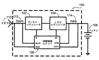
図1は、本発明による、柔軟なバッテリ充電器100のブロック図である。前記バッテリ充電器100は、(ブースト・レギュレータとしても知られている)ブースト充電器102、(LDOレギュレータとしても知られている)LDO充電器104および切替制御ユニット106を持つ。また、バッテリ充電器100には、入力電流を測定するためのアダプタ抵抗112と、充電電流を測定するためのバッテリ抵抗114とを具備していても良い。切替制御ユニット106は、ブースト充電器102とLDO充電器104との両方の動作を制御する。切替制御ユニット106は、アダプタ110であることができる電流ソースからの入力電流と、バッテリ108に流れる充電電流とを監視する。ブースト充電器102は入力電圧を受信し、LDO充電器104はバッテリ108へ充電電流を出力する。バッテリ充電器100は、最初、LDO充電モードでバッテリ108を充電する。バッテリ108の電圧が増加する場合、バッテリ108に供給する充電電流を保持するため、切替制御ユニット106はLDO充電器104の動作を増加させる。バッテリ108の電圧が増加し続けるので、切替制御ユニット106はブースト充電器102をオンにして、ブースト充電モードでバッテリ108を充電する。切替制御ユニット106は、監視ポートichmを通してバッテリ108の電圧と、監視ポートiacpを通してアダプタ110からの電圧とを監視する。
FIG. 1 is a block diagram of a
図2は、本発明の実施形態による、バッテリ充電器100の回路図200である。制御器202は、LDO回路206とブースト回路204との動作を制御する。LDO回路206はLDO充電器104に対応し、ブースト回路204はブースト充電器102に対応する。LDO回路206とブースト回路204とは異なる破線で線引きされ、制御器202は、LDO回路206とブースト回路204の両方により部分的に占められており、二つの充電器が制御器202を共有しているということを象徴している。制御器202は単一チップ・デバイスとして実装されても良く、また、ブースト充電器102およびLDO充電器104と一緒に同じチップに実装されても良い。制御器202はイネーブル・ポイントENを通して有効になり、LDO充電器104とブースト充電器102との動作を同時に制御する。LDO充電器104の電力トランジスタの制御は、電圧Vpbを通して制御器202により行われる。ブースト充電器102の“切替動作”の制御は、切替えポイントLXを通して制御器202によって行われる。
FIG. 2 is a circuit diagram 200 of the
図3は、本発明の一つの実施形態による、バッテリ充電器100の詳細な回路図300である。バッテリ充電器100は、enbポイント302(図2でENとして図示)を通して有効になる。バッテリ充電器100が有効になる前、pbポイント320はiacpポイント318に短絡され、LDO充電器104はOFF条件にとどまり、バッテリ108に流れる充電電流Ichargeは、図4に示すように、ゼロである。
FIG. 3 is a detailed circuit diagram 300 of the
バッテリ充電器100が有効になった後、入力電流が抵抗Rsadp112を通して流れ、電流‘V(iacp、iacm)/Rsadp’は電流検知増幅器304を通過する。電流検知増幅器304から結果として生じる電圧は、誤差増幅器308で、プリセット・アダプタ電流制限値328と比較され、誤差増幅器308からの出力電圧は,図2に示すPMOS FET MP1を制御するVpbを駆動する。
After the
また、電圧Vpb320は誤差増幅器310の出力によっても影響を受ける。Rsbat114が検知する充電電流は電流検知増幅器306を通過し、結果として生じる電圧は、誤差増幅器310でプリセット充電電流制限値330と比較される。図4、5および6から見ることができるように、バッテリ電圧Vichmが充電とともに増加する(図5)ので、電圧Vpbは減少し(図6)、一方、充電電流Icharge(図4)は実質的に一定に保持される。
バッテリがしばらく充電され、バッテリ電圧Vichmがアダプタの電圧Viacpとほぼ同じ電圧に増加した後は、Vpbは連続して減少し、これはバッテリ108を充電するのにもはや効果的でないであろう。この時点で、バッテリ充電器100のブースト・モードが優位に立ち始める。Vpbが、所定のレベル、例えば0.8Vより低いので、比較器314の出力は実効的にパルス幅変調(PWM)信号になり、このPWM信号はNMOS FET326を制御し、これはブースト充電器102に対してスイッチのように働く。比較器314は、入力Vpbおよびランプ信号発生器312が生成したランプ信号を受け取る。
After the battery is charged for a while and the battery voltage Vichm increases to approximately the same voltage as the adapter voltage Viacp, Vpb decreases continuously and this will no longer be effective to charge the
バッテリ電圧Vichmは充電プロセスの間は増加する。バッテリ電圧Vichmが充電電圧のプリセット終点332に達すると、誤差増幅器310の出力はVpb320を増加する。Vpb320が増加するにつれて、充電電流Ichargeは減少する。もしVpb320が、図6に示すように、(0.8Vより高い)ランプ範囲を超えて増加すると、充電プロセスは停止する。
The battery voltage Vichm increases during the charging process. When the battery voltage Vichm reaches the
図7は、本発明の実施形態による、バッテリの充電動作のフローチャート700である。バッテリが本発明のデュアル・モード充電器に接続された後、デュアル・モード充電器はLDOモードでバッテリを充電する(ステップ702)。バッテリがデュアル・モード充電器に接続されている間、バッテリの電圧は常にチェックされている(ステップ704)。バッテリの電圧がアダプタ電圧に非常に近い場合、デュアル・モード充電器はブースト・モードでバッテリを充電し始める(ステップ706)。デュアル・モード充電器の充電モードがLDOモードからブースト・モードに移行する間は、充電電流は一定を保持する。バッテリをブースト・モードで充電する間(ステップ708)、バッテリの電圧は、例えば充電電圧の最終であるプリセット値と比較される(ステップ710)。バッテリの電圧がプリセット値より小さい間は、バッテリはブースト・モードで充電されることを続ける(ステップ708)。バッテリの電圧がプリセット値に達すると、充電動作は停止する(ステップ712)。
FIG. 7 is a
動作では、ユーザは、アダプタ110に接続したバッテリ充電器100を、充電を使い切ったバッテリ108に接続する可能性がある。最初、バッテリ充電器100は、バッテリの電圧がアダプタ110の電圧とほぼ同じ電圧に増加するまで、LDO充電器としてバッテリを充電するであろうが、次に、バッテリ充電器100は、バッテリ108が充電電圧のプリセット終点に達するまでブースト充電器102として動作し始める。本発明である共通制御ループのため、LDO充電器104として動作することからブースト充電器として動作することへの切替えは、スムースであり、緩やかであり、そして自動的である。
In operation, the user may connect the
本方法は何も必要としないし、本特許請求範囲の全ての可能な実施形態を示し教示することは、経済的に禁止的である。それ故に、上記の実施形態は、本開示の原理を明確に理解するために示した実装の単なる典型的な図である。本特許請求項の範囲から逸脱すること無しに、上記で説明した実施形態に変形、修正および組合せを行うことが可能である。そのような変形、修正および組合せは全て、本開示の範囲および以下の特許請求範囲により、本明細書に含まれる。 The method does not require anything, and it is economically prohibitive to show and teach all possible embodiments of the claims. Therefore, the above embodiments are merely exemplary illustrations of implementations shown for a clear understanding of the principles of the present disclosure. Variations, modifications, and combinations may be made to the embodiments described above without departing from the scope of the claims. All such variations, modifications and combinations are included herein by the scope of this disclosure and the following claims.
100 バッテリ充電器
102 ブースト充電器(ブースト・レギュレータ)
104 LDO充電器(LDOレギュレータ)
106 切替制御ユニット
108 バッテリ
110 アダプタ
112 アダプタ抵抗
114 バッテリ抵抗
200 バッテリ充電器の回路図
202 制御器
204 ブースト回路
206 LDO回路
300 バッテリ充電器の詳細な回路図
302 enbポイント
304 電流検知増幅器
306 電流検知増幅器
308 誤差増幅器
310 誤差増幅器
312 ランプ生成器
314 比較器
316 誤差増幅器
318 iacpポイント
320 pbポイント
322 切替えポイント
324 PWM信号
326 NMOS FET
328 プリセット・アダプタ電流制限値
330 プリセット充電電流制限値
332 充電電圧のプリセット終点
700 フローチャート
702 LDOモードでバッテリを充電
704 バッテリの電圧はアダプタ電圧に非常に近いか?
706 充電電流を一定に保持しながら充電モードをブースト・モードに移行
708 ブースト・モードでバッテリを充電
710 バッテリの電圧がプリセット値に達したか?
712 充電動作を停止
100
104 LDO charger (LDO regulator)
106
328 Preset Adapter
706 Transition charge mode to boost mode while keeping charge current constant 708 Charge battery in
712 Stop charging operation
Claims (9)
制御回路と、
制御回路と通信して入力ソースから入力電流を受信するブースト回路と、
制御回路およびブースト回路と通信する低ドロップアウト回路とを備え、
前記ブースト回路はデュアル・モード充電器をブースト・モードで動作させ、
前記低ドロップアウト回路は、充電電流を前記バッテリに出力するとともに、デュアル・モード充電器を低ドロップアウト・モードで動作させ、
制御回路は、前記入力電流と前記充電電流とを監視し、前記入力電流と前記充電電流とに基づいて決定される内部電圧に従ってブースト回路と低ドロップアウト回路とを同時に制御し、デュアル・モード充電器が低ドロップアウト・モードからブースト・モードに切替える間は充電電流を一定に保持し、
前記内部電圧は、第一の端子における電圧であり、前記第一の端子は、前記入力電流を検知するための第一の電流検知増幅器の出力と第一の電流制限値とが入力される第一の誤差増幅器の出力端子と、前記充電電流を検知するための第二の電流検知増幅器の出力と第二の電流制限値とが入力される第二の誤差増幅器の出力端子とに接続されていることを特徴とするデュアル・モード充電器。 A dual mode charger for charging a battery,
A control circuit;
A boost circuit that communicates with the control circuit and receives the input current from the input source;
With a low dropout circuit in communication with the control circuit and boost circuit,
The boost circuit operates the dual mode charger in boost mode,
The low dropout circuit outputs a charging current to the battery and operates the dual mode charger in a low dropout mode;
The control circuit monitors the input current and the charging current, and simultaneously controls the boost circuit and the low dropout circuit according to an internal voltage determined based on the input current and the charging current, and dual mode charging The charging current remains constant while the device switches from low dropout mode to boost mode ,
The internal voltage is a voltage at a first terminal, and the first terminal receives a first current detection amplifier output and a first current limit value for detecting the input current. Connected to an output terminal of one error amplifier and an output terminal of a second error amplifier to which an output of a second current detection amplifier for detecting the charging current and a second current limit value are input. dual-mode charger which is characterized in that there.
ランプ信号を生成するためのランプ信号発生器と、
ランプ信号を前記内部電圧と比較し、比較の結果に基づきパルス幅変調信号を生成するための比較器とを更に備えることを特徴とする請求項1に記載のデュアル・モード充電器。 The control circuit includes a ramp signal generator for generating a ramp signal,
The dual mode charger according to claim 1, further comprising a comparator for comparing a ramp signal with the internal voltage and generating a pulse width modulated signal based on the comparison result.
制御回路と、
制御回路と通信するブースト回路と、
制御回路およびブースト回路と通信する低ドロップアウト回路とを備え、
前記ブースト回路は、入力電流ソースから入力電流を受信し、
前記低ドロップアウト回路は、充電電流をバッテリに出力し、
制御回路は、前記入力電流と前記充電電流とを監視し、前記入力電流と前記充電電流とに基づいて決定される内部電圧に従ってブースト回路と低ドロップアウト回路とを同時に制御し、デュアル・モード充電器は、充電電流を一定に保持しながらブースト回路と低ドロップアウト回路との間で充電動作を切替え、
前記内部電圧は、第一の端子における電圧であり、前記第一の端子は、前記入力電流を検知するための第一の電流検知増幅器の出力と第一の電流制限値とが入力される第一の誤差増幅器の出力端子と、前記充電電流を検知するための第二の電流検知増幅器の出力と第二の電流制限値とが入力される第二の誤差増幅器の出力端子とに接続されていることを特徴とするデュアル・モード充電器。 A dual mode charger for charging a battery,
A control circuit;
A boost circuit communicating with the control circuit;
With a low dropout circuit in communication with the control circuit and boost circuit,
The boost circuit receives input current from an input current source;
The low dropout circuit outputs a charging current to the battery,
The control circuit monitors the input current and the charging current, and simultaneously controls the boost circuit and the low dropout circuit according to an internal voltage determined based on the input current and the charging current, and dual mode charging The device switches the charging operation between the boost circuit and the low dropout circuit while keeping the charging current constant ,
The internal voltage is a voltage at a first terminal, and the first terminal receives a first current detection amplifier output and a first current limit value for detecting the input current. Connected to an output terminal of one error amplifier and an output terminal of a second error amplifier to which an output of a second current detection amplifier for detecting the charging current and a second current limit value are input. dual-mode charger which is characterized in that there.
ことを特徴とする請求項4に記載のデュアル・モード充電器。 5. The dual mode charger according to claim 4 , wherein the control circuit generates a pulse width modulation signal to control the boost circuit.
充電アダプタから入力電流を受信するステップと、
デュアル・モード充電器を低ドロップアウト・モードで動作させるステップと、
充電電流をバッテリに出力するステップと、
バッテリの電圧を充電アダプタの電圧と比較するステップと、
もしバッテリの電圧が充電アダプタの電圧とほぼ同じ電圧であるなら、充電電流を一定に保持しながら、前記入力電流と前記充電電流とに基づいて決定される内部電圧に従ってデュアル・モード充電器を低ドロップアウト・モードからブースト・モードに切替えるステップとを備え、
前記内部電圧は、第一の端子における電圧であり、前記第一の端子は、前記入力電流を検知するための第一の電流検知増幅器の出力と第一の電流制限値とが入力される第一の誤差増幅器の出力端子と、前記充電電流を検知するための第二の電流検知増幅器の出力と第二の電流制限値とが入力される第二の誤差増幅器の出力端子とに接続されていることを特徴とするバッテリを充電する方法。 A method of charging a battery using a dual mode charger, comprising:
Receiving an input current from the charging adapter;
Operating the dual mode charger in low dropout mode;
Outputting charging current to the battery;
Comparing the voltage of the battery with the voltage of the charging adapter;
If the battery voltage is approximately the same as the charging adapter voltage, the dual mode charger is reduced according to the internal voltage determined based on the input current and the charging current while keeping the charging current constant. With a step of switching from dropout mode to boost mode ,
The internal voltage is a voltage at a first terminal, and the first terminal receives a first current detection amplifier output and a first current limit value for detecting the input current. Connected to an output terminal of one error amplifier and an output terminal of a second error amplifier to which an output of a second current detection amplifier for detecting the charging current and a second current limit value are input. method of charging a battery, characterized in that there.
デュアル・モード充電器がバッテリの充電を停止するステップとを更に備えることを特徴とする請求項8に記載のバッテリを充電する方法。 Comparing the battery voltage to the final charge voltage;
9. The method of charging a battery of claim 8 , further comprising the step of the dual mode charger stopping charging the battery.
Applications Claiming Priority (2)
| Application Number | Priority Date | Filing Date | Title |
|---|---|---|---|
| US13/182,765 | 2011-07-14 | ||
| US13/182,765 US8629649B2 (en) | 2011-07-14 | 2011-07-14 | Battery charging apparatus with a common control loop for a low drop-out voltage regulator and a boost regulator |
Publications (2)
| Publication Number | Publication Date |
|---|---|
| JP2013027300A JP2013027300A (en) | 2013-02-04 |
| JP5526185B2 true JP5526185B2 (en) | 2014-06-18 |
Family
ID=46084946
Family Applications (1)
| Application Number | Title | Priority Date | Filing Date |
|---|---|---|---|
| JP2012105205A Active JP5526185B2 (en) | 2011-07-14 | 2012-05-02 | Battery charger with common control loop for low dropout voltage regulator and boost regulator |
Country Status (7)
| Country | Link |
|---|---|
| US (1) | US8629649B2 (en) |
| EP (1) | EP2546949A2 (en) |
| JP (1) | JP5526185B2 (en) |
| KR (1) | KR20130009599A (en) |
| CN (1) | CN102882239B (en) |
| IN (1) | IN2012DE00790A (en) |
| TW (1) | TWI439006B (en) |
Families Citing this family (20)
| Publication number | Priority date | Publication date | Assignee | Title |
|---|---|---|---|---|
| EP2768133B1 (en) | 2013-02-14 | 2015-11-04 | ABB Technology Ltd | Converter cell with reduced power losses, high voltage multilevel converter and associated method |
| US9261934B2 (en) | 2013-03-15 | 2016-02-16 | Intel Corporation | Dynamic response improvement of hybrid power boost technology |
| EP2849020B1 (en) * | 2013-09-13 | 2019-01-23 | Dialog Semiconductor GmbH | A dual mode low dropout voltage regulator |
| KR102231317B1 (en) * | 2013-12-16 | 2021-03-24 | 삼성전자주식회사 | Voltage regulator and power delivering device therewith |
| US9612643B2 (en) | 2014-03-29 | 2017-04-04 | Intel Corporation | Controlling the CPU slew rates based on the battery state of charge |
| TWI544717B (en) | 2014-09-12 | 2016-08-01 | 茂達電子股份有限公司 | Method of setting charging current and charging module |
| JP6144727B2 (en) * | 2015-07-02 | 2017-06-07 | 京セラ株式会社 | Charging apparatus, charging program, and charging method |
| CN107204705B (en) * | 2016-03-18 | 2019-04-19 | 电信科学技术研究院 | The control method of DC-DC adjuster and its soft start, controller |
| CN105871031B (en) * | 2016-05-24 | 2018-08-28 | 无锡中感微电子股份有限公司 | A kind of management of charging and discharging circuit and portable equipment |
| US10476295B2 (en) | 2016-08-22 | 2019-11-12 | Microsoft Technology Licensing, Llc | Charging optimization |
| CN106532831B (en) * | 2016-11-30 | 2018-06-01 | 珠海市魅族科技有限公司 | A kind of charge control method and device |
| CN107482707A (en) * | 2017-07-27 | 2017-12-15 | 太仓华淏信息科技有限公司 | A kind of Portable micro-consumption data collecting system power module |
| US10908218B2 (en) * | 2017-08-01 | 2021-02-02 | Lg Chem, Ltd. | Battery cell management system that detects data misalignment between battery cell voltage values and battery cell overvoltage flags |
| CN108390426B (en) * | 2018-02-07 | 2020-11-20 | 深圳市创新微源半导体有限公司 | Novel lithium battery charging control circuit |
| CN108923649A (en) * | 2018-06-07 | 2018-11-30 | 珠海智融科技有限公司 | A kind of fast charge power supply step-up/step-down circuit and fast charge power supply |
| TWI683502B (en) * | 2018-11-22 | 2020-01-21 | 美律實業股份有限公司 | Charging device and operating method thereof |
| CN110165889A (en) * | 2019-05-21 | 2019-08-23 | 珠海英搏尔电气股份有限公司 | A kind of low dropout voltage regulator device |
| US10996699B2 (en) | 2019-07-30 | 2021-05-04 | Stmicroelectronics Asia Pacific Pte Ltd | Low drop-out (LDO) voltage regulator circuit |
| CN110676913B (en) * | 2019-11-11 | 2023-08-04 | Oppo广东移动通信有限公司 | Charging method, terminal, conversion device and storage medium |
| CN114928128A (en) * | 2022-04-11 | 2022-08-19 | 深圳市道通科技股份有限公司 | Charging circuit and charging device |
Family Cites Families (17)
| Publication number | Priority date | Publication date | Assignee | Title |
|---|---|---|---|---|
| JP4137496B2 (en) * | 2002-04-15 | 2008-08-20 | 富士通株式会社 | Remaining amount prediction method |
| US7459886B1 (en) * | 2004-05-21 | 2008-12-02 | National Semiconductor Corporation | Combined LDO regulator and battery charger |
| DE102004038597B4 (en) * | 2004-08-06 | 2007-10-25 | Texas Instruments Deutschland Gmbh | DC / DC converter with a converter stage and a linear regulator |
| SG124315A1 (en) * | 2005-01-31 | 2006-08-30 | Stl Corp | Battery pack |
| JP2007014163A (en) * | 2005-07-01 | 2007-01-18 | Fujitsu Ltd | Charging ic, charger and electronic apparatus |
| US7880445B2 (en) * | 2006-02-16 | 2011-02-01 | Summit Microelectronics, Inc. | System and method of charging a battery using a switching regulator |
| JP2007323376A (en) | 2006-06-01 | 2007-12-13 | Rohm Co Ltd | Power supply device and electric equipment equipped with the same |
| JP4967526B2 (en) | 2006-08-22 | 2012-07-04 | 富士通セミコンダクター株式会社 | Power supply device control circuit, power supply device and control method therefor |
| CN100559686C (en) * | 2006-09-22 | 2009-11-11 | 立锜科技股份有限公司 | Produce the method and apparatus and the application thereof of pulse width modulating signal |
| JP4308855B2 (en) * | 2007-01-17 | 2009-08-05 | セイコーエプソン株式会社 | Power reception control device, power reception device, and electronic device |
| JP4049333B1 (en) | 2007-01-29 | 2008-02-20 | 株式会社パワーシステム | Charge control device |
| JP5103157B2 (en) | 2007-12-19 | 2012-12-19 | ローム株式会社 | Switching regulator, control circuit thereof, and control method |
| US8217626B2 (en) * | 2008-05-09 | 2012-07-10 | Research In Motion Limited | System and method for dynamic power management of a mobile device |
| US7977921B2 (en) * | 2008-08-15 | 2011-07-12 | National Semiconductor Corporation | AC-to-DC voltage conversion and charging circuitry |
| JP5213621B2 (en) * | 2008-10-02 | 2013-06-19 | ローム株式会社 | Switching regulator control circuit, control method, switching regulator using them, and charging device |
| US8159181B2 (en) * | 2009-02-05 | 2012-04-17 | Infineon Technologies Ag | Combining two or more DC to DC converters to limit external coils |
| US9269993B2 (en) * | 2010-05-04 | 2016-02-23 | Gram Power, Inc. | Rechargeable multipurpose smart power source |
-
2011
- 2011-07-14 US US13/182,765 patent/US8629649B2/en active Active
- 2011-12-23 CN CN201110447201.2A patent/CN102882239B/en active Active
-
2012
- 2012-03-19 IN IN790DE2012 patent/IN2012DE00790A/en unknown
- 2012-04-02 KR KR1020120033895A patent/KR20130009599A/en not_active Application Discontinuation
- 2012-05-02 JP JP2012105205A patent/JP5526185B2/en active Active
- 2012-05-21 EP EP12168691A patent/EP2546949A2/en not_active Withdrawn
- 2012-06-29 TW TW101123563A patent/TWI439006B/en active
Also Published As
| Publication number | Publication date |
|---|---|
| EP2546949A2 (en) | 2013-01-16 |
| US20130015810A1 (en) | 2013-01-17 |
| KR20130009599A (en) | 2013-01-23 |
| TW201304351A (en) | 2013-01-16 |
| CN102882239B (en) | 2014-10-22 |
| IN2012DE00790A (en) | 2015-08-21 |
| JP2013027300A (en) | 2013-02-04 |
| TWI439006B (en) | 2014-05-21 |
| US8629649B2 (en) | 2014-01-14 |
| CN102882239A (en) | 2013-01-16 |
Similar Documents
| Publication | Publication Date | Title |
|---|---|---|
| JP5526185B2 (en) | Battery charger with common control loop for low dropout voltage regulator and boost regulator | |
| US9170591B2 (en) | Low drop-out regulator with a current control circuit | |
| JP5451094B2 (en) | Charging circuit, charging device, electronic device, and charging method | |
| JP4837408B2 (en) | DC-DC converter, control circuit for DC-DC converter, and control method for DC-DC converter | |
| US8129970B2 (en) | Switching regulator with reverse current detection | |
| TWI699068B (en) | Overcurrent protection in a battery charger | |
| JP4324208B2 (en) | Secondary battery charging method and secondary battery protection circuit device | |
| US20110316509A1 (en) | Start-up circuit and method thereof | |
| US20100156518A1 (en) | Dynamic Charge Pump System for Front End Protection Circuit | |
| JP4499966B2 (en) | Secondary battery charging circuit | |
| US10218195B2 (en) | Switching-type charging circuit capable of quickly dropping the voltage at the input end to zero | |
| KR101512535B1 (en) | Battery state monitoring circuit and battery device | |
| US10770894B1 (en) | Fast settlement of supplement converter for power loss protection system | |
| US11239680B2 (en) | Battery charger | |
| KR20060093000A (en) | Current control circuitry and methodology for controlling current from current source | |
| JP5588370B2 (en) | Output circuit, temperature switch IC, and battery pack | |
| US9553461B2 (en) | Charge control circuit, charge circuit, and mobile device | |
| KR101152476B1 (en) | charger and discharer for secondary battery | |
| JP2008061488A (en) | Power supply system equipped with remote control circuit, and method for operating the power supply system | |
| JP4137175B2 (en) | DC-DC converter | |
| US20110254515A1 (en) | Charge control device | |
| WO2016203234A1 (en) | Voltage regulators | |
| US9024574B2 (en) | Battery charger and system method | |
| JP2006020382A (en) | Dc voltage supply | |
| CN113726129B (en) | Power management circuit and electronic equipment |
Legal Events
| Date | Code | Title | Description |
|---|---|---|---|
| A977 | Report on retrieval |
Free format text: JAPANESE INTERMEDIATE CODE: A971007 Effective date: 20130819 |
|
| A131 | Notification of reasons for refusal |
Free format text: JAPANESE INTERMEDIATE CODE: A131 Effective date: 20130827 |
|
| A521 | Request for written amendment filed |
Free format text: JAPANESE INTERMEDIATE CODE: A523 Effective date: 20131101 |
|
| A131 | Notification of reasons for refusal |
Free format text: JAPANESE INTERMEDIATE CODE: A131 Effective date: 20131126 |
|
| A521 | Request for written amendment filed |
Free format text: JAPANESE INTERMEDIATE CODE: A523 Effective date: 20140224 |
|
| TRDD | Decision of grant or rejection written | ||
| A01 | Written decision to grant a patent or to grant a registration (utility model) |
Free format text: JAPANESE INTERMEDIATE CODE: A01 Effective date: 20140317 |
|
| A61 | First payment of annual fees (during grant procedure) |
Free format text: JAPANESE INTERMEDIATE CODE: A61 Effective date: 20140414 |
|
| R150 | Certificate of patent or registration of utility model |
Ref document number: 5526185 Country of ref document: JP Free format text: JAPANESE INTERMEDIATE CODE: R150 |
|
| R250 | Receipt of annual fees |
Free format text: JAPANESE INTERMEDIATE CODE: R250 |
|
| R250 | Receipt of annual fees |
Free format text: JAPANESE INTERMEDIATE CODE: R250 |
|
| R250 | Receipt of annual fees |
Free format text: JAPANESE INTERMEDIATE CODE: R250 |
|
| R250 | Receipt of annual fees |
Free format text: JAPANESE INTERMEDIATE CODE: R250 |
|
| R250 | Receipt of annual fees |
Free format text: JAPANESE INTERMEDIATE CODE: R250 |
|
| R250 | Receipt of annual fees |
Free format text: JAPANESE INTERMEDIATE CODE: R250 |
|
| S111 | Request for change of ownership or part of ownership |
Free format text: JAPANESE INTERMEDIATE CODE: R313113 |
|
| R350 | Written notification of registration of transfer |
Free format text: JAPANESE INTERMEDIATE CODE: R350 |
|
| R250 | Receipt of annual fees |
Free format text: JAPANESE INTERMEDIATE CODE: R250 |
|
| R250 | Receipt of annual fees |
Free format text: JAPANESE INTERMEDIATE CODE: R250 |