US7468636B2 - Radio frequency power amplifier - Google Patents
Radio frequency power amplifier Download PDFInfo
- Publication number
- US7468636B2 US7468636B2 US11/640,866 US64086606A US7468636B2 US 7468636 B2 US7468636 B2 US 7468636B2 US 64086606 A US64086606 A US 64086606A US 7468636 B2 US7468636 B2 US 7468636B2
- Authority
- US
- United States
- Prior art keywords
- radio frequency
- stage transistor
- stage
- frequency power
- former
- Prior art date
- Legal status (The legal status is an assumption and is not a legal conclusion. Google has not performed a legal analysis and makes no representation as to the accuracy of the status listed.)
- Expired - Fee Related, expires
Links
Images


Classifications
-
- H—ELECTRICITY
- H03—ELECTRONIC CIRCUITRY
- H03F—AMPLIFIERS
- H03F1/00—Details of amplifiers with only discharge tubes, only semiconductor devices or only unspecified devices as amplifying elements
- H03F1/56—Modifications of input or output impedances, not otherwise provided for
-
- H—ELECTRICITY
- H03—ELECTRONIC CIRCUITRY
- H03F—AMPLIFIERS
- H03F1/00—Details of amplifiers with only discharge tubes, only semiconductor devices or only unspecified devices as amplifying elements
- H03F1/02—Modifications of amplifiers to raise the efficiency, e.g. gliding Class A stages, use of an auxiliary oscillation
- H03F1/0205—Modifications of amplifiers to raise the efficiency, e.g. gliding Class A stages, use of an auxiliary oscillation in transistor amplifiers
- H03F1/0261—Modifications of amplifiers to raise the efficiency, e.g. gliding Class A stages, use of an auxiliary oscillation in transistor amplifiers with control of the polarisation voltage or current, e.g. gliding Class A
-
- H—ELECTRICITY
- H03—ELECTRONIC CIRCUITRY
- H03F—AMPLIFIERS
- H03F3/00—Amplifiers with only discharge tubes or only semiconductor devices as amplifying elements
- H03F3/60—Amplifiers in which coupling networks have distributed constants, e.g. with waveguide resonators
- H03F3/602—Combinations of several amplifiers
-
- H—ELECTRICITY
- H03—ELECTRONIC CIRCUITRY
- H03H—IMPEDANCE NETWORKS, e.g. RESONANT CIRCUITS; RESONATORS
- H03H7/00—Multiple-port networks comprising only passive electrical elements as network components
- H03H7/38—Impedance-matching networks
- H03H7/383—Impedance-matching networks comprising distributed impedance elements together with lumped impedance elements
-
- H—ELECTRICITY
- H03—ELECTRONIC CIRCUITRY
- H03F—AMPLIFIERS
- H03F2200/00—Indexing scheme relating to amplifiers
- H03F2200/15—Indexing scheme relating to amplifiers the supply or bias voltage or current at the drain side of a FET being continuously controlled by a controlling signal
-
- H—ELECTRICITY
- H03—ELECTRONIC CIRCUITRY
- H03F—AMPLIFIERS
- H03F2200/00—Indexing scheme relating to amplifiers
- H03F2200/168—Two amplifying stages are coupled by means of a filter circuit
-
- H—ELECTRICITY
- H03—ELECTRONIC CIRCUITRY
- H03F—AMPLIFIERS
- H03F2200/00—Indexing scheme relating to amplifiers
- H03F2200/18—Indexing scheme relating to amplifiers the bias of the gate of a FET being controlled by a control signal
-
- H—ELECTRICITY
- H03—ELECTRONIC CIRCUITRY
- H03F—AMPLIFIERS
- H03F2200/00—Indexing scheme relating to amplifiers
- H03F2200/318—A matching circuit being used as coupling element between two amplifying stages
-
- H—ELECTRICITY
- H03—ELECTRONIC CIRCUITRY
- H03F—AMPLIFIERS
- H03F2200/00—Indexing scheme relating to amplifiers
- H03F2200/411—Indexing scheme relating to amplifiers the output amplifying stage of an amplifier comprising two power stages
-
- H—ELECTRICITY
- H03—ELECTRONIC CIRCUITRY
- H03F—AMPLIFIERS
- H03F2200/00—Indexing scheme relating to amplifiers
- H03F2200/451—Indexing scheme relating to amplifiers the amplifier being a radio frequency amplifier
-
- H—ELECTRICITY
- H03—ELECTRONIC CIRCUITRY
- H03F—AMPLIFIERS
- H03F2200/00—Indexing scheme relating to amplifiers
- H03F2200/543—A transmission line being used as coupling element between two amplifying stages
-
- H—ELECTRICITY
- H03—ELECTRONIC CIRCUITRY
- H03F—AMPLIFIERS
- H03F2200/00—Indexing scheme relating to amplifiers
- H03F2200/75—Indexing scheme relating to amplifiers the amplifier stage being a common source configuration MOSFET
Definitions
- the present invention relates to a radio frequency power amplifier suitable for power amplification of a radio frequency signal, which includes a plurality of stages of transistors.
- a radio frequency power amplifier used for wireless communication is desired to be designed to have a low distortion and a high efficiency.
- a quadrature modulation system is used to improve the communication speed, and a communication signal is processed with amplitude modulation in addition to phase modulation in order to suppress frequency dispersion of the modulated signal. Therefore, as a radio frequency power amplifier, a linear amplifier capable of reproducing the amplitude modulation performed on an input signal with high fidelity is used.
- GMSK Global System for Mobile Communications
- a modulated signal is formed by a phase change between two values, i.e., a positive value and a negative value, and so has no amplitude component. Therefore, a radio frequency power amplifier used for the GSM system does not need to reproduce power amplification.
- a radio frequency power amplifier either a linear or a non-linear amplifier is usable. In general, a non-linear amplifier capable of providing a high efficiency is used. In this manner, different types of radio frequency power amplifiers are used for wireless communication in accordance with the modulation system used.
- the efficiency of a radio frequency power amplifier can be improved by increasing the gain compression amount, and can be further improved by matching the harmonic frequency.
- the optimum condition for improving the efficiency effectively varies depending on the control method of an output power of the radio frequency power amplifier or on whether the radio frequency power amplifier is a linear amplifier or a non-linear amplifier.
- non-patent document 1 Inoue, et al., “Analysis of Class-F and Inverse Class-F Amplifiers”, Technical Report of IEICE, ED2000-231, MW2000-180, ICD2000-191 (2001-01)) reports that the efficiency at the time of high gain compression is higher in an inverse class-F amplifier, in which the second harmonic is open and the third harmonic is shortcircuited, than in a class-F amplifier, in which the second harmonic is shortcircuited and the third harmonic is open.
- Non-patent document 2 (“The Efficiency of Class-F and Inverse Class-F Amplifiers”, IEICE Electronic Society (C-10-13) 2004) reports that the efficiency at the time of 1 dB gain compression is higher in an inverse class-F amplifier than in a class-F amplifier when the magnitude of the idle current is large, and is higher in a class-F amplifier than in an inverse class-F amplifier when the magnitude of the idle current is small. In this manner, with radio frequency power amplifiers, the efficiency can be improved by optimally adjusting the matching condition for harmonics in accordance with the communication system.
- a highly efficient non-linear radio frequency power amplifier is used, and two methods are used for controlling the output power thereof.
- the base voltage of the transistor is controlled to vary the power gain and thus to adjust the output power.
- the collector voltage of the transistor is controlled to vary the power gain and thus to adjust the output power.
- the output power is logarithmically varied with respect to the base. voltage. Therefore, the sensitivity of the output power with respect to the base voltage is increased, which makes it difficult to control the output power.
- the output power is varied in a linear function manner with respect to the collector voltage. Therefore, it is easy to control the output power.
- FIG. 9 shows an exemplary basic circuit configuration of a radio frequency power amplifier 101 using the second method.
- the radio frequency power amplifier 101 includes two transistors 102 and 103 connected in a plurality of stages in order to increase the power gain.
- the latter-stage transistor 103 which amplifies a higher level of power, has a larger size. Therefore, the latter-stage transistor 103 has a larger parasitic capacitance or the like than the former-stage transistor 102 , and has a lower impedance than the former-stage transistor 102 .
- an inter-stage matching circuit 104 is provided in order to match the impedance between the collector of the former-stage transistor 102 and the base of the latter-stage transistor 103 .
- the inter-stage matching circuit 104 As a configuration of the inter-stage matching circuit 104 , either a high-pass filter type shown in FIG. 10 which includes a grounded inductor Lp and a capacitor Cs connected thereto in series, or a low-pass filter type shown in FIG. 11 which includes a grounded capacitor Cp and an inductor Ls connected thereto in series, is used. In addition to matching the impedance, the inter-stage matching circuit 104 needs to supply a bias to the collector of the former-stage transistor 102 and to the base of the latter-stage transistor 103 , and also needs to separate the DC components of these bias voltages.
- the inter-stage matching circuit 104 needs to additionally include an impedance conversion device such as a transmission line for supplying a bias, a inductor or the like in order to separate a radio frequency signal and a DC power supply for driving the transistors from each other.
- the inter-stage matching circuit 104 also needs to have a capacitor connected in series in order to separate the collector of the former-stage transistor 102 and the base of the latter-stage transistor 103 from each other. As a result, the circuit scale is enlarged.
- FIG. 12 shows an exemplary conventional radio frequency power amplifier 101 using the high-pass filter type inter-stage matching circuit 104 .
- the inter-stage matching circuit 104 having the high-pass filter type configuration has a characteristic of passing most of the harmonic signal due to a small reflection therein of the harmonic signal.
- the impedance matching of the harmonic signal is not performed by the inter-stage matching circuit 104 .
- the harmonic load impedance characteristic of the former-stage transistor 102 becomes equal to the harmonic load impedance characteristic of the latter-stage transistor 103 .
- the impedance of the harmonic signal is of the low level as the impedance of the latter-stage transistor 103
- the impedance of the fundamental signal is of the high level as the impedance of the former-stage transistor 102 .
- FIG. 13 shows the output power vs. efficiency characteristics of the former-stage transistor 102 in the conventional radio frequency power amplifier 101 using the high-pass filter type inter-stage matching circuit 104 .
- the dashed line represents the relationship between the output power and the efficiency when the base voltage is controlled.
- the solid line represents the relationship between the output power and the efficiency when the collector voltage is controlled.
- the efficiency is gradually reduced when the base voltage is controlled.
- the collector voltage is controlled, there is a region in which the efficiency is rapidly reduced. The cause of this phenomenon will be described with reference to FIG. 14 and FIG. 15 .
- FIG. 14 shows the input power vs. output power characteristics of the conventional radio frequency power amplifier 101 using the high-pass filter type inter-stage matching circuit 104 .
- the horizontal axis represents the input power
- the vertical axis represents the output power.
- a plurality of characteristic lines V 1 through V 6 respectively represent the input vs. output characteristics, which are the characteristics of the output power with respect to the input power to the radio frequency power amplifier, at a plurality of collector voltages.
- the characteristic line V 1 represents the characteristic at the highest collector voltage, and the collector voltage is gradually reduced in the order of the characteristic line V 2 , V 3 , V 4 , V 5 and V 6 .
- the input power of a transmission signal which is input to the radio frequency power amplifier 101 is constant.
- the output power is adjusted along the dashed line by adjusting the collector voltage. It is confirmed that the input vs. output characteristics are in an excessive gain compressed state in a region where the collector voltage is low.
- FIG. 15 shows the input power vs. efficiency characteristics of the former-stage transistor 102 in the conventional radio frequency power amplifier 101 using the high-pass filter type inter-stage matching circuit 104 .
- the horizontal axis represents the input power
- the vertical axis represents the efficiency of the former-stage transistor 102 .
- a plurality of characteristic lines V 1 through V 4 respectively represents the efficiencies with respect to the input power at a plurality of collector voltages.
- the characteristic line V 1 represents the efficiency at the highest collector voltage, and the collector voltage is gradually reduced in the order of the characteristic line V 2 , V 3 and V 4 .
- an object of the present invention is to provide a radio frequency power amplifier capable of adjusting the output power while suppressing the reduction in the efficiency with a system of controlling the collector voltage.
- the present invention is directed to a radio frequency power amplifier including transistors for performing non-linear amplification connected in a plurality of stages.
- the radio frequency power amplifier comprises a former-stage transistor including a base to which a signal is input; a latter-stage transistor including a collector from which the signal is output; and an inter-stage matching circuit for connecting a collector of the former-stage transistor and a base of the latter-stage transistor.
- the inter-stage matching circuit includes a high-pass filter circuit; and an impedance conversion device with which a phase shift of a second harmonic signal is 15 degrees or greater.
- a transmission line, an inductor, or a circuit including an inductor and a capacitor connected in parallel is used.
- the reduction in the power load efficiency of a non-linear transistor for controlling a collector voltage thereof and thus adjusting the output voltage can be suppressed.
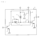
- FIG. 1 shows a schematic configuration of a radio frequency power amplifier 1 according to one embodiment of the present invention
- FIG. 2 shows the input power vs. efficiency characteristics of a former-stage transistor 2 in the radio frequency power amplifier 1 ;
- FIG. 3 shows the output power vs. efficiency characteristics of the former-stage transistor 2 in the radio frequency power amplifier 1 ;
- FIG. 4 shows the relationship between the phase shift of a transmission line m 2 and the reduction in the efficiency
- FIG. 5 through FIG. 8 each show a schematic configuration of a radio frequency power amplifier according to another embodiments of the present invention.
- FIG. 9 shows an exemplary basic circuit configuration of a radio frequency power amplifier 101 ;
- FIG. 10 shows an exemplary configuration of a high-pass filter type inter-stage matching circuit 104 ;
- FIG. 11 shows an exemplary configuration of a low-pass filter type inter-stage matching circuit 104 ;
- FIG. 12 shows an exemplary configuration of the conventional radio frequency power amplifier 101 using the high-pass filter type inter-stage matching circuit 104 ;
- FIG. 13 shows exemplary output power vs. efficiency characteristics of the former-stage transistor 102 in the conventional radio frequency power amplifier 101 ;
- FIG. 14 shows exemplary input power vs. output power characteristics of the former-stage transistor 102 in the conventional radio frequency power amplifier 101 ;
- FIG. 15 shows exemplary input power vs. efficiency characteristics of the former-stage transistor 102 in the conventional radio frequency power amplifier 101 .
- FIG. 1 shows a schematic configuration of a radio frequency power amplifier 1 according to one embodiment of the present invention.
- the radio frequency power amplifier 1 in this embodiment includes a former-stage transistor 2 , a latter-stage transistor 3 , and an inter-stage matching circuit 4 for connecting the former-stagetransistor 2 and the latter-stage transistor 3 .
- the inter-stage matching circuit 4 is a high-pass filter type circuit, and includes transmission lines m 1 and m 2 , and capacitors C 1 and C 2 .
- a radio frequency signal is input to a base, and an amplified radio frequency signal is output from a collector. An emitter of the former-stage transistor 2 is grounded.
- the post-amplification radio frequency signal which is output from the collector of the former-stage transistor 2 is input to a base of the latter-stage transistor 3 via the transmission line m 2 and the capacitor C 2 .
- a connection point of the transmission line m 2 and the capacitor C 2 is supplied with a collector bias via the transmission line m 1 .
- One terminal of the transmission line m 1 which is supplied with the collector bias is grounded via the capacitor C 1 .
- the base of the latter-stage transistor 3 is supplied with a base bias.
- the latter-stage transistor 3 further amplifies the post-amplification radio frequency signal which is input to the base thereof, and then outputs the resultant signal from a collector thereof. An emitter of the latter-stage transistor 3 is grounded.
- a feature of the present invention is that the transmission line m 2 for adjusting the harmonic impedance is provided in the inter-stage matching circuit 4 in order to suppress the reduction in the amplification efficiency.
- the transmission line m 2 has a function of controlling the reflection and passage of a second harmonic signal in the inter-stage matching circuit 4 , and is preferably formed to have a line length with which the phase shift of the second harmonic signal is 15 degrees or greater.
- FIG. 2 shows input power vs. efficiency characteristics of the former-stage transistor 2 in the radio frequency power amplifier 1 when a transmission line m 2 with which the phase is 20 degrees is provided in the inter-stage matching circuit 4 .
- the horizontal axis represents the input power to the former-stage transistor 2
- the vertical axis represents the efficiency of the former-stage transistor 2 .
- a plurality of characteristic lines V 1 through V 4 respectively represent the efficiencies with respect to the input power to the radio frequency power amplifier 1 at a plurality of collector voltages.
- the characteristic line V 1 represents the efficiency at the highest collector voltage, and the collector voltage is gradually reduced in the order of the characteristic line V 2 , V 3 and V 4 .
- FIG. 3 shows the output power vs. efficiency characteristics of the former-stage transistor 2 in the radio frequency power amplifier 1 when the transmission line m 2 with which the phase shift is 20 degrees is provided in the inter-stage matching circuit 4 .
- the dashed line represents the relationship between the output power and the efficiency of the former-stage transistor 2 when the conventional inter-stage matching circuit 104 ( FIG. 12 ) with no transmission line m 2 is used (same as the solid line in FIG. 13 ).
- the solid line represents the relationship between the output power and the efficiency of the former-stage transistor 2 when the inter-stage matching circuit 4 according to the present invention with the transmission line m 2 is used.
- the input power is fixed.
- the efficiency is improved as compared to the conventional case, and there is no region in which the efficiency is rapidly reduced.
- FIG. 4 shows the relationship between the phase shift of the transmission line m 2 and the reduction in the efficiency.
- the horizontal axis represents the phase shift of the second harmonic signal of the transmission line m 2
- the vertical axis represents the ratio between the efficiency at the maximum voltage applied to the collector of the former-stage transistor 2 and the efficiency at half of the maximum voltage applied to the collector of the former-stage transistor 2 .
- the phase shift of the second signal As shown here, as the phase shift of the second signal is increased, the reduction in the efficiency is suppressed. When the phase shift is 15 degrees or greater, the efficiency is kept the same.
- FIG. 5 through FIG. 7 are usable as other exemplary configurations of the inter-stage matching circuit 4 .
- the transmission line m 1 of the inter-stage matching circuit 4 is replaced with an inductor L 1 .
- the transmission lines m 1 and m 2 of the inter-stage matching circuit 4 are respectively replaced with inductors L 1 and L 2 .
- the transmission line m 1 of the inter-stage matching circuit 4 is replaced with an inductor L 1 and the transmission line m 2 is replaced with a parallel circuit of an inductor L 3 and a capacitor C 3 .
- an input circuit 10 may be provided at the base of the former-stage transistor 2 , and an output circuit 20 may be provided at the collector of the latter-stage transistor 3 .
- the input circuit 10 may be a radio frequency power amplifier including at least one stage of transistor.
- the radio frequency power amplifiers 1 shown in the figures are exemplary, and do not limit the present invention. As described above, substantially the same effects are offered by providing an impedance conversion device with which the phase shift of the second harmonic signal is 15 degrees or greater at any position in the inter-stage matching circuit 4 .
Landscapes
- Engineering & Computer Science (AREA)
- Power Engineering (AREA)
- Amplifiers (AREA)
Abstract
Description
Claims (1)
Applications Claiming Priority (2)
| Application Number | Priority Date | Filing Date | Title |
|---|---|---|---|
| JP2005-369503 | 2005-12-22 | ||
| JP2005369503 | 2005-12-22 |
Publications (2)
| Publication Number | Publication Date |
|---|---|
| US20070146077A1 US20070146077A1 (en) | 2007-06-28 |
| US7468636B2 true US7468636B2 (en) | 2008-12-23 |
Family
ID=38192911
Family Applications (1)
| Application Number | Title | Priority Date | Filing Date |
|---|---|---|---|
| US11/640,866 Expired - Fee Related US7468636B2 (en) | 2005-12-22 | 2006-12-19 | Radio frequency power amplifier |
Country Status (1)
| Country | Link |
|---|---|
| US (1) | US7468636B2 (en) |
Cited By (4)
| Publication number | Priority date | Publication date | Assignee | Title |
|---|---|---|---|---|
| US20100277243A1 (en) * | 2009-05-01 | 2010-11-04 | Raytheon Company | Passive spectrum control for pulsed rf power amplifiers |
| US20110081879A1 (en) * | 2009-10-02 | 2011-04-07 | Fujitsu Limited | Amplifier circuit and communication device |
| US10574197B2 (en) * | 2015-12-08 | 2020-02-25 | Mitsubishi Electric Corporation | Multi-stage high frequency amplifier |
| US20210288619A1 (en) * | 2018-07-09 | 2021-09-16 | Sumitomo Electric Industries, Ltd. | Power supply circuit and amplification circuit |
Families Citing this family (3)
| Publication number | Priority date | Publication date | Assignee | Title |
|---|---|---|---|---|
| CN107104684A (en) * | 2017-05-15 | 2017-08-29 | 尚睿微电子(上海)有限公司 | A kind of radio frequency amplification treatment circuit and communication terminal |
| US10530306B2 (en) * | 2018-04-13 | 2020-01-07 | Nxp Usa, Inc. | Hybrid power amplifier circuit or system with combination low-pass and high-pass interstage circuitry and method of operating same |
| CN115606093B (en) * | 2020-06-08 | 2025-08-01 | 三菱电机株式会社 | Amplifying circuit |
Citations (4)
| Publication number | Priority date | Publication date | Assignee | Title |
|---|---|---|---|---|
| US4760348A (en) * | 1987-04-02 | 1988-07-26 | The United States Of America As Represented By The Secretary Of The Navy | Broadband in-line amplifier for submarine antennas |
| JPH0837433A (en) | 1994-05-19 | 1996-02-06 | Matsushita Electric Ind Co Ltd | High frequency power amplifier |
| US5818880A (en) * | 1990-03-30 | 1998-10-06 | Honeywell Inc. | MMIC telemetry transmitter |
| US20020118067A1 (en) * | 2001-02-23 | 2002-08-29 | Nec Corporation | Analog amplifier circuit |
-
2006
- 2006-12-19 US US11/640,866 patent/US7468636B2/en not_active Expired - Fee Related
Patent Citations (4)
| Publication number | Priority date | Publication date | Assignee | Title |
|---|---|---|---|---|
| US4760348A (en) * | 1987-04-02 | 1988-07-26 | The United States Of America As Represented By The Secretary Of The Navy | Broadband in-line amplifier for submarine antennas |
| US5818880A (en) * | 1990-03-30 | 1998-10-06 | Honeywell Inc. | MMIC telemetry transmitter |
| JPH0837433A (en) | 1994-05-19 | 1996-02-06 | Matsushita Electric Ind Co Ltd | High frequency power amplifier |
| US20020118067A1 (en) * | 2001-02-23 | 2002-08-29 | Nec Corporation | Analog amplifier circuit |
Non-Patent Citations (2)
| Title |
|---|
| Akira Inoue, et al., "Analysis of Class-F and Inverse Class-F Amplifiers," Technical Report of IEICE, 2001, pp. 29-35, IEICE. |
| Akira Inoue, et al., "The Efficiency of Class-F and Inverse Class-F Amplifiers," IEICE Electronic Society, 2004, pp. 61. |
Cited By (6)
| Publication number | Priority date | Publication date | Assignee | Title |
|---|---|---|---|---|
| US20100277243A1 (en) * | 2009-05-01 | 2010-11-04 | Raytheon Company | Passive spectrum control for pulsed rf power amplifiers |
| US7868703B2 (en) * | 2009-05-01 | 2011-01-11 | Raytheon Company | Passive spectrum control for pulsed RF power amplifiers |
| US20110081879A1 (en) * | 2009-10-02 | 2011-04-07 | Fujitsu Limited | Amplifier circuit and communication device |
| US8437723B2 (en) * | 2009-10-02 | 2013-05-07 | Fujitsu Limited | Amplifier circuit and communication device |
| US10574197B2 (en) * | 2015-12-08 | 2020-02-25 | Mitsubishi Electric Corporation | Multi-stage high frequency amplifier |
| US20210288619A1 (en) * | 2018-07-09 | 2021-09-16 | Sumitomo Electric Industries, Ltd. | Power supply circuit and amplification circuit |
Also Published As
| Publication number | Publication date |
|---|---|
| US20070146077A1 (en) | 2007-06-28 |
Similar Documents
| Publication | Publication Date | Title |
|---|---|---|
| JP6680235B2 (en) | Power amplifier circuit and high frequency module | |
| CN1934784B (en) | Adaptive bias current circuit of amplifier and current generation method thereof | |
| US6917244B2 (en) | Power control for a switching mode power amplifier | |
| JP5958483B2 (en) | Power amplification module | |
| CN100517960C (en) | Amplifiers, and transmitters and communication devices using the amplifiers | |
| CN101702618A (en) | Gain control of radio frequency linear power amplifier | |
| US9813088B2 (en) | Supply modulators with voltage and frequency partitioning | |
| CN210327513U (en) | Power amplifying circuit | |
| JP4168327B2 (en) | Linear class C amplifier using dynamic bias method | |
| US9024689B2 (en) | Electronic system—radio frequency power amplifier and method for self-adjusting bias point | |
| US7468636B2 (en) | Radio frequency power amplifier | |
| JP2689011B2 (en) | Linear transmitter | |
| JP4714184B2 (en) | Wireless signal amplifier | |
| US7425873B2 (en) | Radio frequency amplification apparatus | |
| US20030201827A1 (en) | High frequency power amplifier module | |
| JP2006501743A (en) | Power amplifier and power amplification method | |
| CN107786170B (en) | Power amplifying circuit | |
| JP2019205006A (en) | Power amplifier circuit | |
| JP2008271172A (en) | High efficiency amplifier | |
| JP5389567B2 (en) | High frequency amplifier and high efficiency method | |
| KR100418180B1 (en) | Power amplifier by using linearizing capacitor | |
| JP2006093857A (en) | Distortion compensation circuit | |
| JP2007195158A (en) | High frequency power amplifier | |
| JP2010148057A (en) | Power amplifier, integrated circuit, and communication apparatus | |
| US9479119B2 (en) | Amplifier circuit and operation method thereof |
Legal Events
| Date | Code | Title | Description |
|---|---|---|---|
| AS | Assignment |
Owner name: MATSUSHITA ELECTRIC INDUSTRIAL CO., LTD., JAPAN Free format text: ASSIGNMENT OF ASSIGNORS INTEREST;ASSIGNORS:MATSUDA, SHINGO;TATEOKA, KAZUKI;MAKIHARA, HIROKAZU;REEL/FRAME:019507/0140 Effective date: 20061205 |
|
| AS | Assignment |
Owner name: PANASONIC CORPORATION, JAPAN Free format text: CHANGE OF NAME;ASSIGNOR:MATSUSHITA ELECTRIC INDUSTRIAL CO., LTD.;REEL/FRAME:021897/0689 Effective date: 20081001 Owner name: PANASONIC CORPORATION,JAPAN Free format text: CHANGE OF NAME;ASSIGNOR:MATSUSHITA ELECTRIC INDUSTRIAL CO., LTD.;REEL/FRAME:021897/0689 Effective date: 20081001 |
|
| FEPP | Fee payment procedure |
Free format text: PAYOR NUMBER ASSIGNED (ORIGINAL EVENT CODE: ASPN); ENTITY STATUS OF PATENT OWNER: LARGE ENTITY |
|
| FPAY | Fee payment |
Year of fee payment: 4 |
|
| AS | Assignment |
Owner name: PANASONIC CORPORATION, JAPAN Free format text: LIEN;ASSIGNOR:COLLABO INNOVATIONS, INC.;REEL/FRAME:031997/0445 Effective date: 20131213 |
|
| AS | Assignment |
Owner name: COLLABO INNOVATIONS, INC., CANADA Free format text: ASSIGNMENT OF ASSIGNORS INTEREST;ASSIGNOR:PANASONIC CORPORATION;REEL/FRAME:033021/0806 Effective date: 20131212 |
|
| REMI | Maintenance fee reminder mailed | ||
| LAPS | Lapse for failure to pay maintenance fees | ||
| STCH | Information on status: patent discontinuation |
Free format text: PATENT EXPIRED DUE TO NONPAYMENT OF MAINTENANCE FEES UNDER 37 CFR 1.362 |
|
| STCH | Information on status: patent discontinuation |
Free format text: PATENT EXPIRED DUE TO NONPAYMENT OF MAINTENANCE FEES UNDER 37 CFR 1.362 |
|
| FP | Lapsed due to failure to pay maintenance fee |
Effective date: 20161223 |