US7463054B1 - Data bus charge-sharing technique for integrated circuit devices - Google Patents
Data bus charge-sharing technique for integrated circuit devices Download PDFInfo
- Publication number
- US7463054B1 US7463054B1 US11/854,422 US85442207A US7463054B1 US 7463054 B1 US7463054 B1 US 7463054B1 US 85442207 A US85442207 A US 85442207A US 7463054 B1 US7463054 B1 US 7463054B1
- Authority
- US
- United States
- Prior art keywords
- voltage
- coupled
- veq
- integrated circuit
- voltage level
- Prior art date
- Legal status (The legal status is an assumption and is not a legal conclusion. Google has not performed a legal analysis and makes no representation as to the accuracy of the status listed.)
- Expired - Fee Related
Links
Images


Classifications
-
- H—ELECTRICITY
- H03—ELECTRONIC CIRCUITRY
- H03K—PULSE TECHNIQUE
- H03K19/00—Logic circuits, i.e. having at least two inputs acting on one output; Inverting circuits
- H03K19/0008—Arrangements for reducing power consumption
Definitions
- the present invention is related to U.S. patent application Ser. No. 11/625,728 filed Jan. 22, 2007 by Michael C. Parris, Douglas B. Butler and Kim C. Hardee for: “Switched Capacitor Charge-Sharing Technique for Integrated Circuit Devices Enabling Signal Generation of Disparate Selected Signal Values”, and U.S. patent application Ser. No. 11/759,823 filed Jun. 7, 2007 by Michael C. Parris and Kim C. Hardee for: “Optimized Charge Sharing for Data Bus Skew Applications”, both of which are assigned to United Memories, Inc., Colorado Springs, Colo. and Sony Corporation, Tokyo, Japan.
- the present invention relates, in general, to the field of semiconductor integrated circuit devices. More particularly, the present invention relates to a data bus charge-sharing technique for integrated circuit devices.
- An integrated circuit device having a large number of internal data buses can have high power dissipation due to the data buses switching at high frequency.
- One way to reduce this power is to reduce the voltage swing on the data buses to a fraction of the power supply voltage, VCC. There are various ways to do this.
- a novel and efficacious charge-sharing technique is disclosed in the aforementioned patent application. Utilizing this technique, charge is shared between two sets of small signal differential precharged data buses. One set of data buses switches between VCC and approximately 0.9 times VCC and the other set of data buses switches between 0.1 times VCC and 0V. In this case the lowest voltage level of one set of data buses is not set equal to the highest voltage level of the second set of data buses. Therefore, new methods of charge-sharing must be utilized.
- a switched capacitor circuit is disclosed as one means for providing the charge-sharing function.
- charge used to drive data lines from VCC to 0.9 times VCC in one set of data buses is also used to drive data lines from 0V to 0.1 times VCC in the second set of data buses. This charge is transferred, in the preferred embodiment, through the switched capacitors.
- the internal voltage levels are determined by the relative capacitances on the two sets of data buses and the switched capacitor. Since this may possibly lead to some uncertainty in establishing these voltage levels, it could also result in increased power and/or insufficient signal levels. Moreover, this particular technique is most particularly applicable for differential precharged data buses and additional circuitry may be required to ensure reliable low frequency operation.
- the charge-sharing technique of the present invention is an alternative to the switched capacitor method disclosed in U.S. patent application Ser. No. 11/625,728.
- two voltage regulators are used to generate constant voltages VEQ 1 and VEQ 2 , which are in the particular exemplary implementation disclosed, approximately 0.9 times VCC and 0.1 times VCC, respectively.
- One set of signals switches between VCC and VEQ 1
- a second set of signals switches between VEQ 2 and 0V. Charge-sharing between the two sets of signals is accomplished by the unique configuration of the voltage regulators.
- an integrated circuit device comprising at least one first signal line capable of switching between a first voltage level and a higher second voltage level, at least one second signal line capable of switching between a differing third voltage level and a lower fourth voltage level and an asynchronous charge-sharing circuit coupled between a source of the first voltage level and a source of the third voltage level.
- Also particularly disclosed herein is a method for operating an integrated circuit device comprising switching at least one first signal line between a first voltage level and a higher second voltage level, switching at least one second signal line between a differing third voltage level and a lower fourth voltage level and sharing charge between a source of the first voltage level and the third voltage level.
- an integrated circuit device including a charge-sharing circuit coupled to first and second signal lines.
- the charge-sharing circuit comprises first and second voltage regulators configured to supply first and second voltage levels at respective outputs thereof.
- a first switching element has an input thereof coupled to the output of the first voltage regulator, with the first switching element being coupled between the first and second signal lines.
- a second switching element has an input thereof coupled to the output of the second voltage regulator, with the second switching element also being coupled between the first and second signal lines.
- an integrated circuit device including a charge-sharing circuit coupled to first and second signal lines.
- the charge sharing circuit comprises first and second voltage regulators configured to supply first and second voltage levels at respective outputs thereof, a switching device coupled between the first and second signal lines and having a control terminal thereof and a logic gate coupled to the outputs of the first and second voltage regulators and having an output thereof coupled to the control terminal of the switching device.
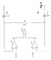
- FIG. 1A is a schematic illustration of a circuit implementing a conventional technique providing small signal swing on two sets of signals without utilizing charge-sharing;
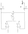
- FIG. 1B is a follow-on schematic illustration of how the VEQ 1 and VEQ 2 generators of the preceding figure might be implemented;
- FIG. 2A is a schematic illustration of a circuit for implementing the data bus charge-sharing technique of the present invention wherein the current flow in the second data state is effectuated between a charge-sharing circuit coupling VEQ 1 and VEQ 2 ;
- FIG. 2B is a schematic illustration of another circuit implementation of the data bus charge-sharing technique of the present invention for use with two sets of differential data buses;
- FIG. 2C is a further schematic illustration of the circuit implementation of the preceding figure but wherein the differential data buses are precharged;
- FIG. 3 is a schematic illustration of a circuit for implementing the charge-sharing technique of the present invention.
- FIG. 4 is a follow-on schematic illustration of a possible circuit implementation for the VEQ 1 and VEQ 2 regulators of the preceding figure;
- FIG. 5 is another schematic illustration of a further possible circuit implementation of the charge-sharing technique of the present invention constituting a modification to the circuit of FIG. 3 ;
- FIG. 6 is a further schematic illustration of still another possible circuit implementation of the charge-sharing technique of the present invention constituting a modification to the circuit of FIG. 4 ;
- FIG. 7 is a schematic illustration of a variation of the circuit of the preceding figure utilizing an N-channel transistor instead of a P-channel device and wherein the inputs to the VEQ 2 comparator are swapped;
- FIG. 8 is a schematic illustration of a variation of the circuit of the preceding figure wherein the lower transistor is removed and the single N-channel transistor is driven by the output of a two-input NOR gate;
- FIG. 9 is a schematic illustration of a variation of the circuit of the preceding figure wherein the single N-channel transistor is replaced with a P-channel device and the NOR gate is replaced with a two-input NAND gate.
- FIG. 1A a schematic illustration of a circuit implementing a conventional technique for providing small signal swing on two sets of signals without utilizing charge-sharing is shown.
- the circuit is initially illustrated in a first data state 100 on the leftmost side of the figure and comprises series connected P-channel transistors 102 and 104 coupled between a source of supply voltage VCC and the output of a VEQ 1 generator 106 .
- the VEQ 1 generator 106 is coupled between VCC and a reference voltage VSS, or circuit ground and provides an output voltage of 0.9 ⁇ VCC.
- a signal transitioning between VCC and 0V is applied to node N 1 at the gate of transistor 102 while a signal substantially simultaneously transitioning between 0V and VCC is applied to node N 2 at the gate of transistor 104 .
- a current I 1 then flows through transistor 102 to a DATA 1 output node intermediate transistors 102 and 104 providing a signal transitioning between a VEQ 1 level of 0.9 ⁇ VCC and VCC as shown.
- the circuit further comprises a VEQ 2 generator 108 coupled between VCC and VSS for providing a VEQ 2 output voltage of 0.1 ⁇ VCC to series connected N-channel transistors 110 and 112 coupled between VEQ 2 and circuit ground. Also as indicated, a signal transitioning between VCC and 0V is applied to node N 3 at the gate of transistor 110 while a signal substantially simultaneously transitioning between 0V and VCC is applied to node N 4 at the gate of transistor 112 . A current I 2 then flows through transistor 112 from a DATA 2 output node intermediate transistors 110 and 112 providing a signal on the DATA 2 output node transitioning between a VEQ 2 level of 0.1 ⁇ VCC and 0V as shown.
- the circuit is also shown in a second data state 120 .
- a signal transitioning from 0V to VCC is applied to node N 1 while a signal transitioning from VCC to 0V is applied to node N 2 .
- a signal transitioning from 0V to VCC is applied to node N 3 while a signal transitioning from VCC to 0V is applied to node N 4 .
- a current I 3 flows from the DATA 1 output through transistor 104 and the VEQ 1 generator 106 to VSS causing an output signal level transitioning from VCC to 0.9 ⁇ VCC as indicated.
- a current I 4 then flows through the VEQ 2 generator 108 and transistor 110 to the DATA 2 output node causing an output signal transitioning from 0V to 0.1 ⁇ VCC.
- the technique illustrated in FIG. 1 implements the provision of small signal swing on two sets of signals, but without charge-sharing.
- the DATA 1 node is representative of a data line in the first set of signals that switch between VCC and VEQ 1 , which is approximately 0.9 times VCC.
- the DATA 2 node is representative of a data line in the second set of signals that switch between 0V and VEQ 2 , which is approximately 0.1 times VCC.
- the first data state 100 shows the DATA 1 node being driven from VEQ 1 to VCC by current I 1 flowing from VCC to DATA 1 through transistor 102 .
- the DATA 2 node is driven from VEQ 2 to 0V by current I 2 flowing from DATA 2 through transistor 112 to VSS.
- the second data state 120 shows the DATA 1 node being driven from VCC to VEQ 1 by current I 3 flowing from DATA 1 to VEQ 1 through transistor 104 .
- the DATA 2 node is driven from 0V to VEQ 2 by current I 4 flowing from VCC to DATA 2 through transistor 110 .
- VEQ 1 and VEQ 2 generators 106 , 108 of the preceding figure might be implemented.
- the VEQ 1 generator 106 comprises a VEQ 1 voltage regulator 122 with an output stage comprising series coupled P-channel transistor 124 and N-channel transistor 126 coupled as a CMOS inverter between VCC and circuit ground.
- a voltage level VEQ 1 of 0.9 ⁇ VCC is provided at the output thereof having a filter capacitor 128 .
- the VEQ 2 generator 108 comprises a VEQ 2 voltage regulator 130 with an output stage comprising series coupled P-channel transistor 132 and N-channel transistor 134 coupled as a CMOS inverter between VCC and circuit ground.
- a voltage level VEQ 2 of 0.1 ⁇ VCC is provided at the output thereof also having a filter capacitor 136 .
- the VEQ 1 regulator 122 senses the level of VEQ 1 and turns on either transistor 124 or 126 to keep the level of VEQ 1 at 0.9 times VCC. Additionally, the VEQ 2 regulator 130 senses the level of VEQ 2 and turns on either transistor 132 or 134 to keep the level of VEQ 2 at 0.1 times VCC. No charge-sharing is provided in this circuit since all of the charge used to hold VEQ 1 and VEQ 2 at the desired levels flows out of the VCC supply and into VSS (circuit ground).
- FIG. 2A a schematic illustration of a circuit for implementing the data bus charge-sharing technique of the present invention is shown wherein the current flow in the second data state is effectuated between a charge-sharing circuit coupling VEQ 1 and VEQ 2 .
- the circuit is initially illustrated in a first data state 200 on the leftmost side of the figure and comprises series connected P-channel transistors 202 and 204 coupled between a source of supply voltage VCC and a VEQ 1 level of 0.9 ⁇ VCC received at one terminal of a charge-sharing circuit 206 .
- the charge-sharing circuit is preferably asynchronous, that is, non-clocked by a clocking signal although one or more enable inputs may still be provided.
- a signal transitioning between VCC and 0V is applied to node N 1 at the gate of transistor 202 while a signal substantially simultaneously transitioning between 0V and VCC is applied to node N 2 at the gate of transistor 204 .
- a current I 1 then flows through transistor 202 to a DATA 1 output node intermediate transistors 202 and 204 providing a signal transitioning between a VEQ 1 level of 0.9 ⁇ VCC and VCC as shown.
- the charge-sharing circuit 206 also has another terminal coupled to a VEQ 2 voltage of 0.1 ⁇ VCC which is provided to series connected N-channel transistors 208 and 210 coupled between VEQ 2 and circuit ground. Also as indicated, a signal transitioning between VCC and 0V is applied to node N 3 at the gate of transistor 208 while a signal substantially simultaneously transitioning between 0V and VCC is applied to node N 4 at the gate of transistor 210 . A current I 2 then flows through transistor 210 from a DATA 2 output node intermediate transistors 208 and 210 providing a signal on the DATA 2 output node transitioning between a VEQ 2 level of 0.1 ⁇ VCC and 0V as shown.
- the circuit is also shown in a second data state 220 .
- a signal transitioning from 0V to VCC is applied to node N 1 while a signal transitioning from VCC to 0V is applied to node N 2 .
- a signal transitioning from 0V to VCC is applied to node N 3 while a signal transitioning from VCC to 0V is applied to node N 4 .
- a current including a shared charge flows from the DATA 1 output node through transistor 204 , the charge-sharing circuit 206 and transistor 208 to the DATA 2 output node.
- the DATA 1 node transitions from VCC to 0.9 ⁇ VCC
- the DATA 2 node transitions from 0V to 0.1 ⁇ VCC.
- This figure illustrates the basic operation of an embodiment of a circuit for implementing the technique of the present invention.
- the current flow is the substantially the same as shown in the preceding figures.
- the current used to drive the DATA 1 node from VCC to VEQ 1 is used to drive the DATA 2 from 0V to VEQ 2 . This is accomplished through the charge-sharing circuit 206 connected between VEQ 1 and VEQ 2 .
- This implementation of the present invention allows, in this particular example, for charge-sharing between sets of single-ended (non-differential) signals.
- the amount of charge-sharing is dependent on the data patterns on one set/of signals with respect to the other set of signals. Ideally the data pattern on one set of signals would be the complement of the other set.
- An application in which this occurs is one in which one set of signals is pipelined and inverted to generate the second set of signals, for example, local data lines and global data lines.
- Another example might be control and address signals that are routed across an integrated circuit chip and then pipelined and re-routed to minimize the total delay.
- FIG. 2B a schematic illustration of another circuit implementation of the data bus charge-sharing technique of the present invention is shown for use with two sets of differential data buses.
- the circuit 230 comprises series coupled P-channel transistors 232 and 234 coupled between VCC and a VEQ 1 level of 0.9 ⁇ VCC received at one terminal of a charge-sharing circuit 240 . As indicated, a signal transitioning between VCC and 0V and back to VCC is applied to node N 1 at the gate of transistor 232 while a signal substantially simultaneously transitioning between 0V and VCC and back to 0V is applied to node N 2 at the gate of transistor 234 .
- the circuit 230 further comprises series coupled P-channel transistors 236 and 238 coupled between VCC and VEQ 1 .
- a signal transitioning between VCC and 0V and back to VCC is applied to node N 3 at the gate of transistor 236 while a signal substantially simultaneously transitioning between 0V and VCC and back to 0V is applied to node N 4 at the gate of transistor 238 .
- the circuit 230 further comprises a VEQ 2 source of 0.1 ⁇ VCC coupled to another terminal of the charge-sharing circuit 240 for providing a VEQ 2 voltage to series coupled N-channel transistors 242 and 244 coupled between VEQ 2 and circuit ground.
- Series coupled N-channel transistors 246 and 248 are also coupled between VEQ 2 and circuit ground.
- a signal transitioning between 0V and VCC and back to 0V is applied to Node N 7 at the gate of transistor 246 while a signal transitioning between VCC to 0V and back to VCC is applied to Node N 8 at the gate of transistor 248 .
- DATA 1 is the complement of DATA 1 B
- DATA 2 is the complement of DATA 2 B.
- the DATA 1 bus transitions between VEQ 1 and VCC and back to VEQ 1 while the DATA 1 B bus transitions between VCC and VEQ 1 and back to VCC.
- the DATA 2 bus transitions between VEQ 2 and 0V and back to VEQ 2 while the DATA 2 B bus transitions between 0V and VEQ 2 and back to 0V.
- FIG. 2C a further schematic illustration of the circuit implementation of the preceding figure is shown wherein the differential data buses are precharged.
- the circuit 250 comprises like structure to that previously described and illustrated and the foregoing description thereof shall suffice herefor.
- the signals input to the nodes N 1 through N 8 are as indicated to provide the output signals on the differential data buses as shown.
- the two sets of differential data buses (DATA 1 /DATA 1 B and DATA 2 /DATA 2 B) are precharged with DATA 1 and DATA 1 B being precharged to VCC, and DATA 2 and DATA 2 B being precharged to VSS.
- the advantage of this particular implementation is that efficient charge-sharing occurs independently of the data patterns of the data buses. Ideally the capacitance on one set of data buses would be substantially equal to the capacitance on the other set of data buses.
- the circuit 300 comprises a VEQ 1 voltage regulator 302 with an output stage comprising P-channel transistor 304 and series coupled N-channel transistor 306 .
- the source terminal of transistor 306 is coupled to the VEQ 2 node.
- the source terminal of transistor 304 is coupled to VCC while the drain terminals of transistors 304 and 306 are coupled to a VEQ 1 node providing an output voltage of substantially 0.9 ⁇ VCC.
- a filter capacitor 308 couples the VEQ 1 node to circuit ground.
- the circuit 300 further comprises a VEQ 2 voltage regulator 310 with an output stage comprising P-channel transistor 312 and series coupled N-channel transistor 314 .
- the source terminal of transistor 312 is coupled to the VEQ 1 node while the drain terminals of transistors 312 and 314 are coupled to a VEQ 2 node providing an output voltage of substantially 0.1 ⁇ VCC.
- the source terminal of transistor 314 is coupled to VSS.
- a filter capacitor 316 couples the VEQ 2 node to circuit ground.
- transistors 306 and 312 effectively implement the charge-sharing operation of the present invention with the source of transistor 306 being coupled to node VEQ 2 instead of VSS, and the source of transistor 312 being coupled to node VEQ 1 instead of VCC. Since charge flows into node VEQ 1 due to DATA 1 switching to VEQ 1 , as shown in FIG. 2A , the voltage of VEQ 1 will tend to rise. If VEQ 1 rises above 0.9 ⁇ VCC, then the VEQ 1 regulator 302 will cause node N 1 ( FIG. 3 ) to go “high”, turning on transistor 306 . Current will then flow from VEQ 1 to VEQ 2 , helping to keep VEQ 1 at 0.9 times VCC.
- VEQ 2 Since charge flows out of node VEQ 2 due to DATA 2 switching to VEQ 2 , then VEQ 2 will tend to fall. If VEQ 2 falls below 0.1 ⁇ VCC, then the VEQ 2 regular 310 will cause node N 2 ( FIG. 3 ) to go “low”, turning on transistor 312 . Current will then flow from node VEQ 1 to VEQ 2 , helping to keep node VEQ 2 at 0.1 ⁇ VCC. In this way, the charge required to drive data line DATA 1 “low” (to VEQ 1 ) is used to drive signal DATA 2 “high” (to VEQ 2 ).
- VEQ 1 goes lower than 0.9 ⁇ VCC
- the VEQ 1 regulator 302 will cause node N 1 ( FIG. 3 ) to go “low”, turning on transistor 304 , which will cause current to flow from VCC to VEQ 1 , raising the level of VEQ 1 .
- VEQ 2 goes higher than 0.1 ⁇ VCC
- the VEQ 2 regulator 310 will cause node N 2 ( FIG. 3 ) to go “high”, turning on transistor 314 , which will cause current to flow from VEQ 2 to VSS, lowering the level of VEQ 2 .
- FIG. 4 a follow-on schematic illustration of a possible circuit implementation for the VEQ 1 and VEQ 2 regulators 302 , 310 of the charge-sharing circuit 300 of the preceding figure is shown.
- the transistors 404 , 406 , 412 and 414 are directly analogous to the transistors 304 , 306 , 312 and 314 of FIG. 3 .
- the filter capacitors 408 and 416 also correspond to the filter capacitors 308 and 316 .
- a voltage comparator 402 with its positive input connected to VEQ 1 and its negative input connected to 0.9 ⁇ VCC is utilized for the VEQ 1 regulator. If the level of VEQ 1 drifts below 0.9 ⁇ VCC then node N 1 goes “low”. If VEQ 1 drifts above 0.9 ⁇ VCC, then node N 1 goes “high”.
- a voltage comparator 410 with its positive input connected to 0.1 ⁇ VCC and its negative input connected to VEQ 2 is utilized for the VEQ 2 regulator. If the level of VEQ 2 drifts above 0.1 ⁇ VCC, then node N 2 goes “high”.
- VEQ 2 drifts below 0.1 ⁇ VCC, then node N 2 goes “low”. It should be noted that any ratio (or fraction) of VEQ 1 and VEQ 2 can be compared to the appropriate ratio (or fraction) of VCC to provide the equivalent functionality.
- FIG. 5 another schematic illustration of a further possible circuit implementation of the charge-sharing technique of the present invention is shown constituting a further modification to the circuit of FIG. 3 .
- the transistors 504 , 506 , 512 and 514 are also directly analogous to the transistors 304 , 306 , 312 and 314 of FIG. 3 .
- the filter capacitors 508 and 516 also correspond to the filter capacitors 308 and 316 .
- the gates of transistors 504 and 506 are connected to difference nodes, N 1 and N 2 .
- Nodes N 1 and N 2 respond slightly differently to the level of VEQ 1 to avoid through-current in the output driver comprising transistors 504 and 506 .
- transistors 512 and 514 are respectively coupled to nodes N 3 and N 4 .
- node N 3 goes “high” before node N 4 goes “high” thereby turning “off” transistor 512 before transistor 514 turns “on”.
- node N 4 goes “low” before node N 3 goes “low” thereby turning “off” transistor 514 before transistor 512 turns “on”.
- FIG. 6 yet another schematic illustration of a further possible circuit implementation of the charge-sharing technique of the present invention is shown constituting a modification to the circuit of FIG. 4 .
- a voltage comparator 602 has the VEQ 1 output level at its positive input and 0.9 ⁇ VCC at its negative input. Output of the comparator 602 on node N 1 is coupled to the gate of an N-channel transistor 604 having its drain terminal coupled to VEQ 1 and its source terminal coupled to VEQ 2 .
- a filter capacitor 606 couples VEQ 1 to circuit ground.
- another voltage comparator 608 has the VEQ 2 output level at its positive input and 0.1 ⁇ VCC at its negative input. Output of the comparator 608 on node N 2 is coupled to the gate of a P-channel transistor 610 having its source terminal coupled to VEQ 1 and its drain terminal coupled to VEQ 2 . A filter capacitor 612 couples VEQ 2 to circuit ground.
- VEQ 1 and VEQ 2 there is no pull-up transistor on VEQ 1 and no pull-down transistor on VEQ 2 .
- the voltage levels on VEQ 1 and VEQ 2 are determined by the relative capacitances on DATA 1 and DATA 2 (e.g. FIG. 2A ).
- the advantage of this configuration is more efficient charge-sharing while a possible downside is the relative uncertainty of the voltage levels of VEQ 1 and VEQ 2 .
- FIG. 7 a schematic illustration of a variation of the circuit of the preceding figure is shown utilizing an N-channel transistor 710 instead of a P-channel device ( 610 , FIG. 6 ) and wherein the inputs to the VEQ 2 comparator are swapped.
- comparator 702 corresponds to comparator 602 , transistor 704 to transistor 604 , capacitor 706 to capacitor 606 , comparator 708 to comparator 608 and capacitor 712 to capacitor 612 .
- the circuit 700 shown is the fundamentally the same as the circuit 600 of FIG. 6 except that P-channel transistor 610 is replaced with N-channel transistor 710 . Also, the inputs of the VEQ 2 comparator 708 are swapped. This circuit provides improved transfer of charge between VEQ 1 and VEQ 2 due to inherently higher transconductance of N-channel transistors compared to P-channel devices.
- the circuit 800 comprises a voltage comparator 802 with its negative input coupled to VEQ 1 and its positive input coupled to 0.9 ⁇ VCC. Output of the comparator 802 on node N 1 is supplied as one input to a two-input NOR gate 804 which has its output coupled to the gate terminal of an N-channel transistor 806 coupled between VEQ 1 and VEQ 2 .
- Another voltage comparator 810 has its positive input coupled to VEQ 2 wand its negative input coupled to 0.1 ⁇ VCC. Its output at node N 2 is coupled to the other input of the NOR gate 804 .
- Filter capacitors 808 and 812 respectively couple the VEQ 1 and VEQ 2 lines to circuit ground.
- circuit 800 transistor 710 ( FIG. 7 ) has been omitted and the gate of transistor 806 is coupled to the output of NOR gate 804 with its inputs connected to nodes N 1 and N 2 .
- the outputs of the VEQ 1 and VEQ 2 comparators 802 , 810 are combined to turn transistor 806 “on” and “off”.
- the configuration of circuit 800 comprises a simplification of the circuit illustrated and described with respect to FIG. 7 .
- FIG. 9 a schematic illustration of a variation of the circuit of the preceding figure is shown wherein the single N-channel transistor ( 806 , FIG. 8 ) is replaced with a P-channel device and the NOR gate is replaced with a two-input NAND gate.
- the circuit 900 comprises a voltage comparator 902 with its positive input coupled to VEQ 1 and its negative input coupled to 0.9 ⁇ VCC. Output of the comparator 902 on node N 1 is supplied as one input to a two-input NAND gate 904 which has its output coupled to the gate terminal of a P-channel transistor 906 coupled between VEQ 1 and VEQ 2 . Another voltage comparator 910 has its negative input coupled to VEQ 2 wand its positive input coupled to 0.1 ⁇ VCC. Its output at node N 2 is coupled to the other input of the NAND gate 904 . Filter capacitors 908 and 912 respectively couple the VEQ 1 and VEQ 2 lines to circuit ground.
- the circuit 900 is similar to the circuit 800 in FIG. 8 . except transistor 906 is now a P-channel device and the NOR gate 804 ( FIG. 8 ) is now replaced with a NAND gate 904 . Also as can be seen, the inputs to the comparators 902 and 910 have been swapped.
- the terms “comprises”, “comprising”, or any other variation thereof, are intended to cover a non-exclusive inclusion, such that a process, method, article, or apparatus that comprises a recitation of certain elements does not necessarily include only those elements but may include other elements not expressly recited or inherent to such process, method, article or apparatus. None of the description in the present application should be read as implying that any particular element, step, or function is an essential element which must be included in the claim scope and THE SCOPE OF THE PATENTED SUBJECT MATTER IS DEFINED ONLY BY THE CLAIMS AS ALLOWED. Moreover, none of the appended claims are intended to invoke paragraph six of 35 U.S.C. Sect. 112 unless the exact phrase “means for” is employed and is followed by a participle.
Landscapes
- Physics & Mathematics (AREA)
- Engineering & Computer Science (AREA)
- Computer Hardware Design (AREA)
- Computing Systems (AREA)
- General Engineering & Computer Science (AREA)
- Mathematical Physics (AREA)
- Logic Circuits (AREA)
Abstract
Description
Claims (24)
Priority Applications (2)
| Application Number | Priority Date | Filing Date | Title |
|---|---|---|---|
| US11/854,422 US7463054B1 (en) | 2007-09-12 | 2007-09-12 | Data bus charge-sharing technique for integrated circuit devices |
| JP2007333605A JP4674305B2 (en) | 2007-09-12 | 2007-12-26 | Data bus charge sharing technology for integrated circuit devices |
Applications Claiming Priority (1)
| Application Number | Priority Date | Filing Date | Title |
|---|---|---|---|
| US11/854,422 US7463054B1 (en) | 2007-09-12 | 2007-09-12 | Data bus charge-sharing technique for integrated circuit devices |
Publications (1)
| Publication Number | Publication Date |
|---|---|
| US7463054B1 true US7463054B1 (en) | 2008-12-09 |
Family
ID=40090578
Family Applications (1)
| Application Number | Title | Priority Date | Filing Date |
|---|---|---|---|
| US11/854,422 Expired - Fee Related US7463054B1 (en) | 2007-09-12 | 2007-09-12 | Data bus charge-sharing technique for integrated circuit devices |
Country Status (2)
| Country | Link |
|---|---|
| US (1) | US7463054B1 (en) |
| JP (1) | JP4674305B2 (en) |
Cited By (4)
| Publication number | Priority date | Publication date | Assignee | Title |
|---|---|---|---|---|
| US20130027283A1 (en) * | 2011-07-29 | 2013-01-31 | Stmicroelectronics S.R.L | Charge-sharing path control device for a scan driver of an lcd panel |
| US20150109051A1 (en) * | 2007-12-31 | 2015-04-23 | Son H. Lam | Supply voltage control based at least in part on power state of integrated circuit |
| WO2015105984A1 (en) * | 2014-01-09 | 2015-07-16 | Qualcomm Incorporated | Charge sharing linear voltage regulator |
| US20220321123A1 (en) * | 2020-10-09 | 2022-10-06 | Metis Microsystems | Circuits and Methods to harvest energy from transient on-chip data |
Families Citing this family (1)
| Publication number | Priority date | Publication date | Assignee | Title |
|---|---|---|---|---|
| US7649406B2 (en) * | 2007-09-13 | 2010-01-19 | United Memories, Inc. | Short-circuit charge-sharing technique for integrated circuit devices |
Citations (8)
| Publication number | Priority date | Publication date | Assignee | Title |
|---|---|---|---|---|
| US6115316A (en) * | 1998-06-29 | 2000-09-05 | Fujitsu Limited | Semiconductor memory device with overdriven sense amplifier and stabilized power-supply circuit of source follower type |
| US6259322B1 (en) * | 1999-10-28 | 2001-07-10 | Texas Instruments Incorporated | Current efficient, ultra low noise differential gain amplifier architecture |
| US6347058B1 (en) * | 2000-05-19 | 2002-02-12 | International Business Machines Corporation | Sense amplifier with overdrive and regulated bitline voltage |
| US6487133B2 (en) * | 2000-07-05 | 2002-11-26 | Kabushiki Kaisha Toshiba | Semiconductor device |
| US6754122B2 (en) * | 2002-02-05 | 2004-06-22 | Kabushiki Kaisha Toshiba | Semiconductor memory device having overdriven bit-line sense amplifiers |
| US6949954B2 (en) * | 2001-10-11 | 2005-09-27 | California Institute Of Technology | Method and apparatus for an asynchronous pulse logic circuit |
| US20070040580A1 (en) * | 2005-08-18 | 2007-02-22 | Texas Instruments Incorporated | Reference buffer with improved drift |
| US20070279100A1 (en) * | 2006-05-31 | 2007-12-06 | Fujitsu Limited | Recycling Charge to Reduce Energy Consumption During Mode Transition in Muiltithreshold Complementary Metal-Oxide-Semiconductor (MTCMOS) Circuits |
Family Cites Families (2)
| Publication number | Priority date | Publication date | Assignee | Title |
|---|---|---|---|---|
| US6476642B1 (en) * | 2000-07-17 | 2002-11-05 | Agere Systems Guardian Corp. | Differential current driver circuit |
| US7085950B2 (en) * | 2001-09-28 | 2006-08-01 | Koninklijke Philips Electronics N.V. | Parallel data communication realignment of data sent in multiple groups |
-
2007
- 2007-09-12 US US11/854,422 patent/US7463054B1/en not_active Expired - Fee Related
- 2007-12-26 JP JP2007333605A patent/JP4674305B2/en not_active Expired - Fee Related
Patent Citations (8)
| Publication number | Priority date | Publication date | Assignee | Title |
|---|---|---|---|---|
| US6115316A (en) * | 1998-06-29 | 2000-09-05 | Fujitsu Limited | Semiconductor memory device with overdriven sense amplifier and stabilized power-supply circuit of source follower type |
| US6259322B1 (en) * | 1999-10-28 | 2001-07-10 | Texas Instruments Incorporated | Current efficient, ultra low noise differential gain amplifier architecture |
| US6347058B1 (en) * | 2000-05-19 | 2002-02-12 | International Business Machines Corporation | Sense amplifier with overdrive and regulated bitline voltage |
| US6487133B2 (en) * | 2000-07-05 | 2002-11-26 | Kabushiki Kaisha Toshiba | Semiconductor device |
| US6949954B2 (en) * | 2001-10-11 | 2005-09-27 | California Institute Of Technology | Method and apparatus for an asynchronous pulse logic circuit |
| US6754122B2 (en) * | 2002-02-05 | 2004-06-22 | Kabushiki Kaisha Toshiba | Semiconductor memory device having overdriven bit-line sense amplifiers |
| US20070040580A1 (en) * | 2005-08-18 | 2007-02-22 | Texas Instruments Incorporated | Reference buffer with improved drift |
| US20070279100A1 (en) * | 2006-05-31 | 2007-12-06 | Fujitsu Limited | Recycling Charge to Reduce Energy Consumption During Mode Transition in Muiltithreshold Complementary Metal-Oxide-Semiconductor (MTCMOS) Circuits |
Non-Patent Citations (2)
| Title |
|---|
| Rajapandian, Saravanan, Shepard, Kenneth L., Hazucha, Peter, Karnik, Tanay, High-Voltage Power Delivery Through Charge Recycling, IEEE Journal of Solid-State Circuits, vol. 41, No. 6, Jun. 2006, pp. 1400-1410. |
| Yamauchi, Hiroyuki, Akamatsu, Hironori, Fujita, Tsutomu, An Asymptotically Zero Power Charge-Recycling Bus Architecture for Battery-Operated Ultrahigh Data Rate ULSI's, IEEE Journal of Solid-State Circuits, vol. 30, No. 4, Apr. 1995, pp. 423-431. |
Cited By (13)
| Publication number | Priority date | Publication date | Assignee | Title |
|---|---|---|---|---|
| US9342126B2 (en) * | 2007-12-31 | 2016-05-17 | Intel Corporation | Supply voltage control based at least in part on power state of integrated circuit |
| US20150109051A1 (en) * | 2007-12-31 | 2015-04-23 | Son H. Lam | Supply voltage control based at least in part on power state of integrated circuit |
| US8878758B2 (en) * | 2011-07-29 | 2014-11-04 | Stmicroelectronics S.R.L. | Charge-sharing path control device for a scan driver of an LCD panel |
| US20130027283A1 (en) * | 2011-07-29 | 2013-01-31 | Stmicroelectronics S.R.L | Charge-sharing path control device for a scan driver of an lcd panel |
| US9645591B2 (en) | 2014-01-09 | 2017-05-09 | Qualcomm Incorporated | Charge sharing linear voltage regulator |
| CN105900036A (en) * | 2014-01-09 | 2016-08-24 | 高通股份有限公司 | Charge sharing linear voltage regulator |
| WO2015105984A1 (en) * | 2014-01-09 | 2015-07-16 | Qualcomm Incorporated | Charge sharing linear voltage regulator |
| CN105900036B (en) * | 2014-01-09 | 2018-05-29 | 高通股份有限公司 | charge sharing linear voltage regulator |
| US20220321123A1 (en) * | 2020-10-09 | 2022-10-06 | Metis Microsystems | Circuits and Methods to harvest energy from transient on-chip data |
| US20230112781A1 (en) * | 2020-10-09 | 2023-04-13 | Metis Microsystems | Circuits and Methods to use energy harvested from transient on-chip data |
| US20230268923A1 (en) * | 2020-10-09 | 2023-08-24 | Metis Microsystems, Llc | Circuits & methods to harvest energy from transient data |
| US11984887B2 (en) * | 2020-10-09 | 2024-05-14 | Metis Microsystems, Llc | Circuits and methods to use energy harvested from transient on-chip data |
| US11984888B2 (en) * | 2020-10-09 | 2024-05-14 | Metis Microsystems, Llc | Circuits and methods to harvest energy from transient on-chip data |
Also Published As
| Publication number | Publication date |
|---|---|
| JP4674305B2 (en) | 2011-04-20 |
| JP2009071798A (en) | 2009-04-02 |
Similar Documents
| Publication | Publication Date | Title |
|---|---|---|
| US7248075B2 (en) | Level shifter with low leakage current | |
| US8154323B2 (en) | Output driver operable over wide range of voltages | |
| US7317335B2 (en) | Level shifter with low leakage current | |
| US6677797B2 (en) | Semiconductor integrated circuit | |
| KR100419816B1 (en) | Signal potential conversion circuit | |
| JP2001284535A (en) | Semiconductor integrated circuit | |
| US5696722A (en) | Level-shifter, semiconductor integrated circuit, and control methods thereof | |
| CA2201853A1 (en) | High voltage level shifter for switching high voltage in non-volatile memory integrated circuits | |
| US20070176650A1 (en) | High-speed, low-power input buffer for integrated circuit devices | |
| US20100194453A1 (en) | Semiconductor device | |
| US7463054B1 (en) | Data bus charge-sharing technique for integrated circuit devices | |
| KR100211758B1 (en) | Multi-power data buffer | |
| JPH10163826A (en) | Driving method of CMOS inverter and Schmitt trigger circuit | |
| KR100567497B1 (en) | Bus interface circuit and receiver circuit | |
| US6466054B2 (en) | Level converter circuit | |
| JP2009509449A (en) | Single threshold, single conductivity type logic circuit | |
| US6563351B2 (en) | Semiconductor integrated circuit having output buffer | |
| US6707703B2 (en) | Negative voltage generating circuit | |
| US7924086B2 (en) | Boosting circuit | |
| US7609570B2 (en) | Switched capacitor charge sharing technique for integrated circuit devices enabling signal generation of disparate selected signal values | |
| CN114420175A (en) | Power supply circuit and non-volatile memory chip | |
| KR100210734B1 (en) | Logic and lever converter and semiconductor device | |
| US7570106B2 (en) | Substrate voltage generating circuit with improved level shift circuit | |
| JPS63111720A (en) | Output buffer circuit | |
| JP2007149207A (en) | Semiconductor integrated circuit device |
Legal Events
| Date | Code | Title | Description |
|---|---|---|---|
| AS | Assignment |
Owner name: UNITED MEMORIES, INC., COLORADO Free format text: ASSIGNMENT OF ASSIGNORS INTEREST;ASSIGNORS:HARDEE, KIM C.;PARRIS, MICHAEL C.;REEL/FRAME:019819/0101 Effective date: 20070911 Owner name: SONY CORPORATION, JAPAN Free format text: ASSIGNMENT OF ASSIGNORS INTEREST;ASSIGNORS:HARDEE, KIM C.;PARRIS, MICHAEL C.;REEL/FRAME:019819/0101 Effective date: 20070911 |
|
| AS | Assignment |
Owner name: SONY CORPORATION, JAPAN Free format text: CORRECTIVE ASSIGNMENT TO CORRECT THE ASSIGNEE ADDRESS, PREVIOUSLY RECORDED ON REEL 019819 FRAME 0101;ASSIGNORS:HARDEE, KIM C.;PARRIS, MICHAEL C.;REEL/FRAME:020357/0683 Effective date: 20070911 Owner name: UNITED MEMORIES, INC., COLORADO Free format text: CORRECTIVE ASSIGNMENT TO CORRECT THE ASSIGNEE ADDRESS, PREVIOUSLY RECORDED ON REEL 019819 FRAME 0101;ASSIGNORS:HARDEE, KIM C.;PARRIS, MICHAEL C.;REEL/FRAME:020357/0683 Effective date: 20070911 |
|
| STCF | Information on status: patent grant |
Free format text: PATENTED CASE |
|
| FEPP | Fee payment procedure |
Free format text: PAYOR NUMBER ASSIGNED (ORIGINAL EVENT CODE: ASPN); ENTITY STATUS OF PATENT OWNER: LARGE ENTITY |
|
| CC | Certificate of correction | ||
| FPAY | Fee payment |
Year of fee payment: 4 |
|
| AS | Assignment |
Owner name: SONY CORPORATION, JAPAN Free format text: ASSIGNMENT OF ASSIGNORS INTEREST;ASSIGNOR:UNITED MEMORIES INC.;REEL/FRAME:030967/0231 Effective date: 20100128 |
|
| FPAY | Fee payment |
Year of fee payment: 8 |
|
| FEPP | Fee payment procedure |
Free format text: MAINTENANCE FEE REMINDER MAILED (ORIGINAL EVENT CODE: REM.); ENTITY STATUS OF PATENT OWNER: LARGE ENTITY |
|
| LAPS | Lapse for failure to pay maintenance fees |
Free format text: PATENT EXPIRED FOR FAILURE TO PAY MAINTENANCE FEES (ORIGINAL EVENT CODE: EXP.); ENTITY STATUS OF PATENT OWNER: LARGE ENTITY |
|
| STCH | Information on status: patent discontinuation |
Free format text: PATENT EXPIRED DUE TO NONPAYMENT OF MAINTENANCE FEES UNDER 37 CFR 1.362 |
|
| FP | Lapsed due to failure to pay maintenance fee |
Effective date: 20201209 |