US7450348B2 - Electronic device, magnetoresistance effect element; magnetic head, recording/reproducing apparatus, memory element and manufacturing method for electronic device - Google Patents
Electronic device, magnetoresistance effect element; magnetic head, recording/reproducing apparatus, memory element and manufacturing method for electronic device Download PDFInfo
- Publication number
- US7450348B2 US7450348B2 US10/875,838 US87583804A US7450348B2 US 7450348 B2 US7450348 B2 US 7450348B2 US 87583804 A US87583804 A US 87583804A US 7450348 B2 US7450348 B2 US 7450348B2
- Authority
- US
- United States
- Prior art keywords
- electrode
- metal conductor
- magnetoresistance effect
- effect element
- magnetization
- Prior art date
- Legal status (The legal status is an assumption and is not a legal conclusion. Google has not performed a legal analysis and makes no representation as to the accuracy of the status listed.)
- Expired - Fee Related, expires
Links
Images


Classifications
-
- G—PHYSICS
- G11—INFORMATION STORAGE
- G11B—INFORMATION STORAGE BASED ON RELATIVE MOVEMENT BETWEEN RECORD CARRIER AND TRANSDUCER
- G11B5/00—Recording by magnetisation or demagnetisation of a record carrier; Reproducing by magnetic means; Record carriers therefor
- G11B5/127—Structure or manufacture of heads, e.g. inductive
- G11B5/33—Structure or manufacture of flux-sensitive heads, i.e. for reproduction only; Combination of such heads with means for recording or erasing only
- G11B5/39—Structure or manufacture of flux-sensitive heads, i.e. for reproduction only; Combination of such heads with means for recording or erasing only using magneto-resistive devices or effects
- G11B5/3903—Structure or manufacture of flux-sensitive heads, i.e. for reproduction only; Combination of such heads with means for recording or erasing only using magneto-resistive devices or effects using magnetic thin film layers or their effects, the films being part of integrated structures
-
- B—PERFORMING OPERATIONS; TRANSPORTING
- B82—NANOTECHNOLOGY
- B82Y—SPECIFIC USES OR APPLICATIONS OF NANOSTRUCTURES; MEASUREMENT OR ANALYSIS OF NANOSTRUCTURES; MANUFACTURE OR TREATMENT OF NANOSTRUCTURES
- B82Y10/00—Nanotechnology for information processing, storage or transmission, e.g. quantum computing or single electron logic
-
- B—PERFORMING OPERATIONS; TRANSPORTING
- B82—NANOTECHNOLOGY
- B82Y—SPECIFIC USES OR APPLICATIONS OF NANOSTRUCTURES; MEASUREMENT OR ANALYSIS OF NANOSTRUCTURES; MANUFACTURE OR TREATMENT OF NANOSTRUCTURES
- B82Y30/00—Nanotechnology for materials or surface science, e.g. nanocomposites
-
- G—PHYSICS
- G11—INFORMATION STORAGE
- G11B—INFORMATION STORAGE BASED ON RELATIVE MOVEMENT BETWEEN RECORD CARRIER AND TRANSDUCER
- G11B5/00—Recording by magnetisation or demagnetisation of a record carrier; Reproducing by magnetic means; Record carriers therefor
- G11B5/127—Structure or manufacture of heads, e.g. inductive
- G11B5/33—Structure or manufacture of flux-sensitive heads, i.e. for reproduction only; Combination of such heads with means for recording or erasing only
- G11B5/39—Structure or manufacture of flux-sensitive heads, i.e. for reproduction only; Combination of such heads with means for recording or erasing only using magneto-resistive devices or effects
- G11B5/3903—Structure or manufacture of flux-sensitive heads, i.e. for reproduction only; Combination of such heads with means for recording or erasing only using magneto-resistive devices or effects using magnetic thin film layers or their effects, the films being part of integrated structures
- G11B5/3906—Details related to the use of magnetic thin film layers or to their effects
-
- G—PHYSICS
- G11—INFORMATION STORAGE
- G11C—STATIC STORES
- G11C11/00—Digital stores characterised by the use of particular electric or magnetic storage elements; Storage elements therefor
- G11C11/02—Digital stores characterised by the use of particular electric or magnetic storage elements; Storage elements therefor using magnetic elements
- G11C11/14—Digital stores characterised by the use of particular electric or magnetic storage elements; Storage elements therefor using magnetic elements using thin-film elements
- G11C11/15—Digital stores characterised by the use of particular electric or magnetic storage elements; Storage elements therefor using magnetic elements using thin-film elements using multiple magnetic layers
-
- H—ELECTRICITY
- H10—SEMICONDUCTOR DEVICES; ELECTRIC SOLID-STATE DEVICES NOT OTHERWISE PROVIDED FOR
- H10N—ELECTRIC SOLID-STATE DEVICES NOT OTHERWISE PROVIDED FOR
- H10N50/00—Galvanomagnetic devices
- H10N50/01—Manufacture or treatment
-
- H—ELECTRICITY
- H10—SEMICONDUCTOR DEVICES; ELECTRIC SOLID-STATE DEVICES NOT OTHERWISE PROVIDED FOR
- H10N—ELECTRIC SOLID-STATE DEVICES NOT OTHERWISE PROVIDED FOR
- H10N50/00—Galvanomagnetic devices
- H10N50/10—Magnetoresistive devices
-
- H—ELECTRICITY
- H10—SEMICONDUCTOR DEVICES; ELECTRIC SOLID-STATE DEVICES NOT OTHERWISE PROVIDED FOR
- H10N—ELECTRIC SOLID-STATE DEVICES NOT OTHERWISE PROVIDED FOR
- H10N99/00—Subject matter not provided for in other groups of this subclass
- H10N99/05—Devices based on quantum mechanical effects, e.g. quantum interference devices or metal single-electron transistors
Definitions
- the present invention relates to an electronic device having a fine shape controlled in the nanometer order, a magnetoresistance effect element having a fine shape controlled in the nanometer order; a magnetic head, a recording/reproducing apparatus, a memory element and a memory array using the magnetoresistance effect element; a method for manufacturing the electronic device; and a method for manufacturing the magnetoresistance effect element.
- a nanotechnology for controlling the structure of a material on the order of nanometers has been valued as a basic technology of information and communication, etc., and research and development have been carried out actively.
- magnetic devices and electronic devices having a fine shape controlled on the order of nanometers have been proposed.
- the resistance of the TMR element is inversely proportional to the square of the TMR element width, which is proportional to the track width of an information recording medium. Since the width of the TMR element becomes narrower as the recording density is higher and the track width is narrower, the resistance of the TMR element becomes extremely high. Therefore, it is difficult to apply the element to the fine structured magnetic head.
- MRAM magnetic resistance memory
- TMR film a magnetic resistance memory (MRAM) using a TMR film
- the MR ratio of the magnetic resistance memory using the TMR film is about 50%, which is insufficient as a memory element.
- the MR ratio is reported to be 100,000% at room temperature (see Physical Review B67, 2003, p60401, which hereinafter will be referred to as non-patent document 5)
- the conductivity of the carbon nano-tube differs depending upon the chirality, so that it is difficult to control the formed carbon nano-tube becoming an arm-chair type exhibiting a property of metal property or a zigzag type exhibiting a property of a semiconductor or a chiral type exhibiting a property of an insulator.
- a nano-contact portion formed of plating has a structure that cannot be controlled. Therefore, it is not possible to use it practically.
- an object of the present invention to provide an electronic device having a fine shape controlled on the order of nanometers, a magnetoresistance effect element; a magnetic head, a recording/reproducing apparatus, a memory element and a memory array using the magnetoresistance effect element; a method for manufacturing the electronic device; and a method for manufacturing the magnetoresistance effect element.
- the first electronic device of the present invention includes a first electrode and a second electrode; and a metal conductor thin film electrically connected to the first electrode and the second electrode.
- the metal conductor thin film comprises a metal conductor portion that bridges a gap between the first electrode and the second electrode seen from the direction perpendicular to the bottom surfaces of the first electrode and the second electrode; a bridge length L of the metal conductor portion is not more than a mean free path ⁇ of electron in the metal conductor portion at the operation temperature of the electronic device.
- the electronic device is manufactured by: forming the first electrode and the second electrode on a substrate with a gap having the bridge length L; forming a support that includes at least one selected from the group consisting of a nano-tube and a nano-wire and bridges a gap between the first electrode and the second electrode seen from the direction perpendicular to the bottom surfaces; and forming the metal conductor portion by a method of depositing the metal conductor thin film on the support and on the first electrode and the second electrode.
- the phrase “mean free path ⁇ of electron” denotes a distance in which electron can travel without being scattered.
- the phrase “bridge length L of a metal conductor portion” denotes a length along the central axis from a point P 1 in which a cross-sectional area along the central axis of the electronic device rapidly is decreased to a point P 2 in which a cross-sectional area of the electronic device rapidly is increased.
- the method for measuring the bridge length L of the metal conductor portion will be explained in detail in the embodiments.
- the first electronic device according to the present invention is manufactured by forming the first electrode and the second electrode on the substrate with a gap having the bridge length L that is not more than a mean free path ⁇ of electron in the metal conductor portion at the operation temperature of the electronic device; forming a support that includes at least one selected from the group consisting of a nano-tube and a nano-wire and bridges a gap between the first electrode and the second electrode seen from the direction perpendicular to the bottom surfaces; and forming the metal conductor portion by a method of depositing the metal conductor thin film on the support, on the first electrode and the second electrode, it is possible to form the metal conductor portion having the bridge length L that is not more than the mean free path ⁇ of electron on the support including at least one selected from the group consisting of a nano-tube and a nano-wire.
- the metal conductor portion of the present invention is formed of metal, unlike the carbon nano-tube described in non-patent document 4 that is not capable of controlling the conductivity, the metal conductor portion of the present invention has a stable conductivity. Furthermore, the contact resistance to the first electrode and the second electrode becomes extremely small. Therefore, the electric property becomes stable.
- the electronic device is manufactured by a process of depositing the metal conductor thin film and then removing the support. By removing the support that is not capable of controlling the conductivity, the electric property of the electronic device is more stable.
- the electronic device may be manufactured by a process of depositing the metal conductor thin film and then removing the substrate.
- the CNT is used for the substrate, since the CNT of the substrate shows three kinds of properties of a conductor, a semiconductor and an insulator, by removing the substrate composed of CNT, the electric property of the electronic device becomes more stable.
- the first electrode and the second electrode comprise a magnetic substance. It is advantageous because the electronic device can be used as a magnetoresistance effect element and a memory element.
- the first electrode and the second electrode comprise at least one element selected from the group consisting of Fe, Co and Ni. It is advantageous because it is possible to obtain a magnetoresistance effect element and a memory element having an excellent magnetic property.
- the metal conductor thin film comprises a magnetic substance. Since a magnetic domain wall can be pinned to the metal conductor portion, it is possible to obtain a magnetoresistance effect element that operates in accordance with either the presence or absence of the magnetic domain wall.
- the metal conductor thin film comprises at least one element selected from the group consisting of Fe, Co and Ni.
- the magnetic domain wall can be pinned on the metal conductor portion securely.
- the cross-sectional area Si of the first electrode, the cross-sectional area S 2 of the second electrode and the cross-sectional area S 3 of the metal conductor portion satisfy the following relationship: S 3 ⁇ S 1 and S 3 ⁇ S 2 .
- the magnetic domain wall can be pinned on the metal conductor portion securely.
- the cross-sectional area S 3 of the metal conductor portion is 1 nm 2 or more and 1.0 ⁇ 10 6 nm 2 or less.
- the cross-sectional area S 3 is less than 1 nm 2 , it tends to be difficult to form the metal conductor portion controlled on the order of nanometers with high reproducibility.
- the cross-sectional area S 3 is more than 1.0 ⁇ 10 6 nm 2 , it tends to be difficult to realize the quantum conductance.
- the support comprises a carbon nano-tube.
- a carbon nano-tube it is possible to control a fine shape of the support easily. Furthermore, it is possible to precisely control the shape of the metal conductor portion in a desirable manner. Since the carbon nano-tube has high thermal resistance as compared with a material such as protein nano-wire, etc. containing an organic substance and has high mechanical strength, it can be manufactured easily.
- the step of forming the support comprises providing a catalyst for promoting the formation reaction of the carbon nano-tube on the first electrode and the second electrode; and forming the support comprising the carbon nano-tube by a chemical vapor deposition (CVD) method.
- the carbon nano-tube can be produced easily.
- the step of forming the support comprises forming the support comprising the carbon nano-tube while applying different voltages to the first electrode and the second electrode, respectively. It is advantageous because an electric field is provided between the first electrode and the second electrode, thus making it possible to form the carbon-nano tube easily.
- the first electrode and the second electrode comprise a magnetic substance; and the catalyst comprises at least one element selected from the group consisting of Fe, Co and Ni. Since Fe, Co and Ni are magnetic substances, if the magnetic substances remain in the first and second electrodes after the electronic device is manufactured, the electric property and the magnetic property are not deteriorated.
- the support may comprise at least one of a self-organizable protein nano-wire and silicon nano-wire.
- a fine shape of the support can be controlled precisely.
- a fine shape of the metal conductor portion can be controlled to a desirable shape precisely.
- the step for forming the metal conductor portion comprises depositing the metal conductor thin film by a physical vapor deposition (PVD) method.
- PVD physical vapor deposition
- an operation temperature of the electronic device is 4.2 K or more and 523 K or less. If the operation temperature is less than 4.2 K, a system for cooling the electronic device tends to be complicated, and the cost tends to rise greatly because of using an expensive cooling medium such as liquid He. If the operation temperature is more than 523 K, peripheral equipment (peripheral equipment such as semiconductor element, magnetic medium, etc. used in combination of the electronic device) that can be used at an operation temperature of more than 523 K is extremely limited. Therefore, peripheral equipment that is excellent in weather resistance (thermal resistance, etc.) must be used.
- the operation temperature is 4.2 K or more and 523 K or less
- the cross-sectional area of the metal conductor portion by controlling the cross-sectional area of the metal conductor portion by the use of the quantum conductance, while using an advantage of the present invention, that is, it is possible to avoid the variation in conductivity that occurred when the conductivity with respect to the cross sectional area of the metal conductor portion shows continuous values, the performance of the other peripheral equipment can be ensured. Thus, a desirable performance of the apparatus as a whole can be obtained.
- the second electronic device of the present invention includes a first electrode and a second electrode; and a metal conductor that bridges a gap between the first electrode and the second electrode.
- the bridge length L of the metal conductor portion is not more than a mean free path ⁇ of electron in the metal conductor at the operation temperature of the electronic device.
- the electronic device is manufactured by: forming the first electrode and the second electrode on a substrate with a gap having the bridge length L; forming a support that includes at least one selected from the group consisting of a nano-tube and a nano-wire and bridges a gap between the first electrode and the second electrode; and depositing the metal conductor on the support.
- the first electrode and the second electrode are formed on the substrate with a gap having the bridge length L; the support that includes at least one selected from the group consisting of a nano-tube and a nano-wire and bridges a gap between the first electrode and the second electrode is formed; and the metal conductor is deposited on the support. It is possible to form the metal conductor that has the bridge length L that is not more than the mean free path ⁇ of electron and directly bridges the first electrode and the second electrode on the support that includes at least one selected from the group consisting of the nano-tube and the nano-wire and directly bridges between the first electrode and the second electrode.
- the metal conductor in the metal conductor, a phenomenon called quantum conductance appears.
- the metal conductor is different from the carbon nano-tube described in the non-patent document 4 and has a stable conductivity. Furthermore, the contact resistance to the first electrode and the second electrode is reduced. Therefore, by using the quantum conductance, by controlling the cross sectional area of the metal conductor portion, an electronic device free from variation in conductivity can be obtained.
- the third electronic device of the present invention includes a first electrode film; an insulating film formed on the first electrode film; a second electrode film formed on the insulating film; and a metal conductor penetrating the insulating film and electrically connecting the first electrode film and the second electrode film.
- the length L of the metal conductor is not more than a mean free path ⁇ of electron in the metal conductor at the operation temperature of the electronic device.
- the electronic device is manufactured by: forming the first electrode film on the substrate; forming the insulating film on the first electrode film to the thickness that is the length L of the metal conductor; providing the insulating film with a through hole reaching the first electrode thin film by irradiating the insulating film with a field emission electron beam from a probe of a scanning tunneling microscope (STM) that includes at least one selected from the group consisting of a nano-tube and a nano-wire; filling the inside of the through hole with the metal conductor; and forming the second electrode film on the insulating film and the metal conductor.
- STM scanning tunneling microscope
- the electronic device is manufactured by forming the first electrode film on the substrate; forming the insulating film on the first electrode film to the thickness that is the length L of the metal conductor; providing the insulating film with the through hole reaching the first electrode thin film by irradiating the insulating film with the field emission electron beam from the probe of the scanning tunneling microscope (STM) that includes at least one selected from the group consisting of the nano-tube and the nano-wire; filling the inside of the through hole with the metal conductor; and forming the second electrode film on the insulating film and the metal conductor film.
- STM scanning tunneling microscope
- the through hole formed by irradiating with field emission beams from the probe of STM including at least one selected from the group consisting of the nano-tube and the nano-wire it is possible to manufacture a metal conductor having the length L of not more than the mean free path ⁇ of electron.
- a phenomenon occurs called quantum conductance in which the conductivity (conductance) with respect to the cross-sectional area changes stepwise, and a phenomenon occurs called ballistic conduction in which an electron passes through the metal conductor without being scattered appear.
- the metal conductor of the present invention is formed of metal, unlike the carbon nano-tube described in the non-patent document 4 that is not capable of controlling the conductivity, it has stable conductivity. Furthermore, the contact resistance to the first electrode film and the second electrode film is greatly reduced. Therefore, the electric property becomes stable.
- the cross-sectional area of the metal conductor by using the quantum conductance, it is possible to obtain an electronic device capable of avoiding the variation of the conductivity occurred when the conductivity with respect to the cross-sectional area is linearly changed. Furthermore, by controlling the magnetization directions of the first electrode film and the second electrode film, the magnetoresistance effect element having an extremely high MR ratio may be obtained owing to the ballistic conduction.
- the fourth electronic device includes a first electrode and a second electrode; and an insulating film formed in contact with the first electrode and the second electrode between the first electrode and the second electrode.
- the insulating film is provided with a groove that reaches from the first electrode to the second electrode; the groove is filled with the metal conductor that is brought into contact with the first electrode and the second electrode; and the length L of the metal conductor is not more than a mean free path ⁇ of electron in the metal conductor at the operation temperature of the electronic device.
- the electronic device is manufactured by forming the first electrode and the second electrode on a substrate arranged with a gap having the length L. The insulating film is in brought into contact with the first electrode and the second electrode between the first electrode and the second electrode on the substrate.
- the insulating film is provided with the groove reaching from the first electrode to the second electrode by irradiating the insulating film with a field emission electron beam from a probe of the scanning tunneling microscope (STM) that includes at least one selected from the group consisting of a nano-tube and a nano-wire; and filling the groove with the metal conductor.
- STM scanning tunneling microscope
- the fourth electronic device of the present invention is manufactured by forming the first electrode and the second electrode on the substrate arranged with a gap having the bridge length L.
- the insulating film is brought into contact with the first electrode and the second electrode between the first electrode and the second electrode on the substrate.
- the insulating film is provided with the groove reaching from the first electrode thin film to the second electrode thin film by irradiating the insulating film with a field emission electron beam from the probe of the scanning tunneling microscope STM that includes at least one selected from the group consisting of the nano-tube and the nano-wire; and filling the groove with the metal conductor.
- the groove formed by irradiating with field emission beams from the probe of STM including at least one selected from the group consisting of the nano-tube and the nano-wire it is possible to manufacture a metal conductor having the length L of not more than the mean free path ⁇ of electron.
- a phenomenon occurs called quantum conductance in which the conductivity (conductance) with respect to the cross-sectional area changes stepwise, and a phenomenon occurs called ballistic conduction in which an electron passes through the metal conductor without being scattered appear.
- the metal conductor of the present invention is formed of metal, unlike the carbon nano-tube described in the non-patent document 4 that is not capable of controlling the conductivity, it has stable conductivity. Furthermore, the contact resistance to the first electrode film and the second electrode film is extremely reduced. Therefore, the electric property becomes stable.
- the cross-sectional area of the metal conductor by using the quantum conductance, it is possible to obtain an electronic device capable of avoiding the variation of the conductivity that occurrs when the conductivity with respect to the cross-sectional area is linearly changed. Furthermore, by controlling the magnetization directions of the first electrode and the second electrode, the magnetoresistance effect element having an extremely high MR ratio may be obtained owing to the ballistic conduction.
- the first electrode and the second electrode comprise a magnetic substance; and the metal conductor is provided with a concave portion.
- a magnetic domain wall can be pinned to the site of the concave portion of the metal conductor securely.
- a portion in which the cross-sectional area rapidly is decreased can be formed in the metal conductor portion, and the position of the magnetic domain wall can be fixed to this site.
- the magnetoresistance effect element includes a first electrode and a second electrode comprising a magnetic substance; and a metal conductor thin film electrically connected to the first electrode and the second electrode.
- the metal conductor thin film comprises a metal conductor portion that bridges a gap between the first electrode and the second electrode seen from the direction perpendicular to the bottom surfaces of the first electrode and the second electrode.
- the bridge length L of the metal conductor portion is not more than a value that is a larger value of the value of the length of electron spin diffusion in the metal conductor portion at the operation temperature of the magnetoresistance effect element and the value of mean free path ⁇ of electron in the metal conductor portion at the operation temperature of the magnetoresistance effect element.
- the cross-sectional area S 1 of the first electrode, the cross-sectional area S 2 of the second electrode and the cross-sectional area S 3 of the metal conductor portion satisfy the following relationship: S 3 ⁇ S 1 and S 3 ⁇ S 2 .
- the magnetoresistance effect element is manufactured by: forming the first electrode and the second electrode on the substrate with a gap having the bridge length L; forming a support that includes at least one selected from a group consisting of a nano-tube and a nano-wire and bridges a gap between the first electrode and the second electrode seen from the direction perpendicular to the bottom surfaces; and forming the metal conductor portion by a method of depositing the metal conductor thin film on the support, on the first electrode and the second electrode.
- the “length of electron spin diffusion” in the present invention is the distance in which an electron can travel with the magnetization state (up spin state or down spin state) maintained.
- the electronic device is manufactured by forming the first electrode and the second electrode on the substrate with a gap having the bridge length L, which is not more than a value that is the larger of the value of the length of electron spin diffusion in the metal conductor portion at the operation temperature of the magnetoresistance effect element and the value of mean free path ⁇ of electron in the metal conductor portion at the operation temperature of the magnetoresistance effect element; forming the support that includes at least one selected from the group consisting of the nano-tube and the nano-wire and bridges the gap between the first electrode and the second electrode seen from the direction perpendicular to the bottom surfaces; and forming the metal conductor portion by the method of depositing the metal conductor thin film on the support, on the first electrode and the second electrode.
- the metal conductor portion of the present invention is formed of metal, it has a stable conductivity unlike the carbon nano-tube described in the non-patent document 3 that is not capable of controlling the conductivity. Furthermore, the contact resistance between the first electrode and the second electrode becomes extremely small. Therefore, the electric property becomes stable.
- the magnetoresistance effect element having an extremely high MR ratio can be obtained owing to the ballistic conduction.
- the magnetoresistance effect element is manufactured by depositing the metal conductor thin film and then removing the support. By removing the support that is not capable of controlling the conductivity, the electric property can be more stable. Furthermore, it is possible to reduce the contact resistance between the first electrode and the metal conductor portion and the contact resistance between the second electrode and the metal conductor portion can be reduced further.
- the magnetoresistance effect element can be manufactured by a step of removing the substrate after depositing the metal conductor thin film.
- the CNT of the substrate shows three kinds of properties of a conductor, a semiconductor and an insulator, and by removing the substrate composed of CNT, the electric property of the magnetoresistance effect element becomes more stable.
- the first electrode comprises a free layer in which the magnetization is rotated easily with respect to an external magnetic field
- the second electrode comprises a pinned layer in which the magnetization is not rotated easily with respect to an external magnetic field
- the magnetization easy axis of the free layer is perpendicular to the direction of the external magnetic field to be detected.
- the magnetization is rotated easily with respect to an external magnetic field
- the magnetization is not rotated easily with respect to an external magnetic field denote respectively that the free layer is magnetization-rotated with respect to the external magnetic field applied to the magnetoresistance effect element but the pinned layer is not magnetization-rotated.
- the pinned layer comprises an antiferromagnetic film; and a magnetic layer is formed on the antiferromagnetic film and pinned by the antiferromagnetic film, wherein the magnetic film is electrically connected to the metal conductor portion.
- the property (MR ratio) of the magnetoresistance effect element is thermally stable.
- the support includes a carbon nano-tube.
- the carbon nano-tube it is possible to control a fine shape of the support easily. Furthermore, a fine shape of the metal conductor portion can be controlled to a desirable shape precisely. Since the carbon nano-tube has high thermal resistance and high mechanical strength as compared with, for example, a protein nano-wire, etc. that is a material including an organic material, it can be manufactured easily.
- the step of forming the support comprises providing a catalyst for promoting the formation reaction of the carbon nano-tube to the first electrode and the second electrode, and forming the support comprising the carbon nano-tube by a chemical vapor deposition (CVD) method. It is possible to form a carbon nano-tube easily.
- CVD chemical vapor deposition
- the step for forming the support comprises forming the support comprising the carbon nano-tube while applying different voltages to the first electrode and the second electrode, respectively. It is possible to form a carbon nano-tube easily by forming an electric field between the first electrode and the second electrode.
- the catalyst comprises at least one element selected from the group consisting of Fe, Co and Ni. Since Fe, Co and Ni are magnetic substances, even if the magnetic substance remains in the first and second electrodes after being manufactured, the electric property and magnetic property cannot be deteriorated.
- the support may comprise at least one of a self-organizable protein nano-wire and silicon nano-wire.
- a self-organizable protein nano-wire By controlling DNA of the protein nano-wire, the fine shape of the support can be controlled precisely. Furthermore, a fine shape of the metal conductor portion can be controlled to a desirable shape precisely.
- the step for forming the metal conductor portion comprises depositing the metal conductor thin film by a physical vapor deposition (PVD) method.
- PVD physical vapor deposition
- the metal conductor thin film comprises at least one selected from the group consisting of Fe, Co and Ni.
- a magnetic domain wall can be pinned to the metal conductor portion securely.
- the first electrode and the second electrode comprise at least one element selected from the group consisting of Fe, Co and Ni.
- a magnetoresistance effect element having an excellent magnetic property can be obtained.
- an operation temperature of the magnetoresistance effect element is 4.2 K or more and 523 K or less. If the operation temperature is less than 4.2K, a system for cooling the electronic device tends to be complicated, and the cost tends to rise greatly because of using an expensive cooling medium such as liquid He. If the operation temperature is more than 523 K, peripheral equipment (peripheral equipment such as semiconductor element, magnetic medium, etc. used in combination of the electronic device) that can be used at an operation temperature of more than 523 K is extremely limited. Therefore, peripheral equipment that is excellent in weather resistance (thermal resistance, etc.) must be used.
- the operation temperature is 4.2 K or more and 523 K or less
- an advantage of the present invention that is, it is possible to obtain high MR ratio easily and securely, the performance of the other peripheral equipment can be ensured.
- a desirable performance of the apparatus as a whole can be ensured.
- the magnetic head according to the present invention includes a magnetoresistance effect element according to the present invention; a first lead wire electrically connected to the first electrode of the magnetoresistance effect element; and a second lead wire electrically connected to the second electrode of the magnetoresistance effect element.
- the magnetic head according to the present invention is provided with a magnetoresistance effect element according to the present invention having a high MR ratio of 100% or more. Therefore, it is possible to obtain an extremely high sensitivity and an extremely high output.
- the recording/reproducing apparatus includes a recording head for recording information in a magnetic media; and a reproducing head for reproducing information recorded on the magnetic media.
- the reproducing head is a magnetic head of the present invention.
- the magnetoresistance effect element of the present invention having an extremely high MR ratio of 100% or more is provided as the reproducing head. Therefore, it is possible to carry out high output with the recording head and to reproduce information recorded in the magnetic medium with high recording density of 100 Gb/inch 2 or more easily and precisely.
- the first memory element of the present invention includes a magnetoresistance effect element according to the present invention.
- the first electrode of the magnetoresistance effect element comprises a free layer in which the magnetization is rotated easily with respect to an external magnetic field
- the second electrode comprises a pinned layer in which the magnetization is not rotated easily with respect to the external magnetic field.
- the memory element further comprises a word line generating an external magnetic field that changes the magnetization directions of the free layer and the pinned layer in parallel or in anti-parallel, based on an electric current; and an electric current supplier for supplying the word line with the electric current.
- the magnetoresistance effect element is a magnetoresistance effect element of the present invention, an extremely high MR ratio can be realized as compared with a conventional magnetoresistance effect element having the MR ratio of about 60%.
- the second memory element of the present invention includes a magnetoresistance effect element according to the present invention, and an electric current supplier for supplying either an electric current flowing in the metal conductor portion from the first electrode toward the second electrode, or an electric current flowing in the metal conductor portion from the second electrode toward the first electrode.
- an electric current supplier for supplying either an electric current flowing in the metal conductor portion from the first electrode toward the second electrode, or an electric current flowing in the metal conductor portion from the second electrode toward the first electrode.
- the magnetoresistance effect element is a magnetoresistance effect element of the present invention, an extremely high MR ratio can be realized as compared with a conventional magnetoresistance effect element having the MR ratio of about 60%.
- the second memory element does not require a word line as a component element as in the first memory element of the present invention, a configuration can be made to be small and simple.
- a memory element that has a simple and small-sized configuration in which the cell area is small, the space for installing the memory is small and the recording density is high.
- the current density of the electric current supplied to the magnetoresistance effect element by the electric current supplier is 1.0 ⁇ 10 5 A/cm 2 or more.
- the current density of the electric current supplied to the magnetoresistance effect element is 1.0 ⁇ 10 5 A/cm 2 or more, information can be written in the magnetoresistance effect element easily and securely.
- the current density is less than 1.0 ⁇ 10 5 A/cm 2 , information cannot written securely.
- the memory array of the present invention includes magnetoresistance effect elements according to the present invention arranged in a matrix; wiring for writing information in magnetoresistance effect elements independently and reading out the information; a write unit for writing information in the magnetoresistance effect element independently via the wiring by inverting the direction of the electric current flowing in the metal conductor portion of the magnetoresistance effect element so as to change the magnetization directions of the first electrode and the second electrode in parallel or in anti parallel; and a read unit for reading out independently the information written in the magnetoresistance effect element via the wiring by measuring the resistance value of the magnetoresistance effect element that is different depending upon the magnetization directions of the first electrode and the second electrode.
- the memory array of the present invention a plurality of magnetoresistance effect elements of the second memory element of the present invention are provided. Like the second memory element of the present invention, the memory array does not need a word line. Therefore, it is possible to realize a memory element that has a simple and small-sized configuration in which the cell area is small, the space for installing the memory is small and the recording density is high.
- the method for manufacturing an electronic device of the present invention includes forming a first electrode and a second electrode on a substrate with a gap L therebetween; forming a support that includes at least one selected from a nano-tube and a nano-wire and that bridges a gap between the first electrode and the second electrode seen from the direction perpendicular to the bottom surfaces of the first electrode and the second electrode; and forming a metal conductor portion that bridges a gap between the first electrode and the second electrode seen from the direction perpendicular to the bottom surface by a method of depositing a metal conductor thin film on the support, on the first electrode and the second electrode.
- the gap L is not more than the mean free path ⁇ of electron in the metal conductor portion at the operation temperature of the electronic device.
- a phenomenon occurs called a quantum conductance in which the conductivity (conductance) changes stepwise with respect to the cross sectional area of the metal conductor portion is observed.
- the metal conductor portion of the present invention is formed of metal, unlike the carbon nano-tube described in the non-patent document 4 that is not capable of controlling the conductivity, it has stable conductivity. Furthermore, the contact resistance between the first electrode and the second electrode is extremely reduced. Therefore, the electric property becomes stable.
- the method for manufacturing the magnetoresistance effect element of the present invention includes forming a first electrode and a second electrode comprising a magnetic substance on a substrate with a gap L therebetween; forming a support that comprises at least one selected from the group consisting of a nano-tube and a nano-wire and that bridges a gap between the first electrode and the second electrode seen from the direction perpendicular to the bottom surfaces of the first electrode and the second electrode; and forming a metal conductor portion that bridges a gap to the first electrode and the second electrode seen from the direction perpendicular to the bottom surfaces of the first electrode and the second electrode by a method of depositing a metal conductor thin film on the support, on the first electrode and the second electrode.
- the gap L is not more than a value that is the larger of the value of the length of electron spin diffusion in the metal conductor portion at the operation temperature of the magnetoresistance effect element and the value of mean free path ⁇ of electron in the metal conductor portion at the operation temperature of the magnetoresistance effect element.
- the cross-sectional area S 1 of the first electrode, the cross-sectional area S 2 of the second electrode and the cross-sectional area S 3 of the metal conductor portion satisfy the following relationship: S 3 ⁇ S 1 and S 3 ⁇ S 2 .
- the metal conductor portion having a bridge length L that is the larger of the value of the length of electron spin diffusion and the value of mean free path ⁇ of electron is formed on the support having at least one selected from the group consisting of the nano-tube and the nano-wire.
- the metal conductor portion of the present invention is formed of metal, it has a stable conductivity unlike a carbon nano-tube described in the non-patent document 3 that is not capable of controlling the conductivity. Furthermore, the contact resistance to the first electrode and the second electrode becomes extremely small. Thus, the electric property becomes stable.
- an electronic device having a fine shape controlled on the order of nanometers, a magnetoresistance effect element; a magnetic head, a recording/reproducing apparatus, a memory element and a memory array using the magnetoresistance effect element; a method for manufacturing the electronic device; and a method for manufacturing the magnetoresistance effect element.
- FIG. 1A is a plan view showing an electronic device according to Embodiment 1.
- FIG. 1B is a cross-sectional view taken along a line 1 B- 1 B of FIG. 1A .
- FIG. 1C is a cross-sectional view taken along a line 1 C- 1 C of FIG. 1B .
- FIG. 1D is a cross-sectional view to explain a method for manufacturing the electronic device according to Embodiment 1.
- FIG. 1E is a cross-sectional view to explain a method for manufacturing the electronic device according to Embodiment 1.
- FIG. 2A is a cross-sectional view showing an electronic device to explain a method for measuring the bridge length L of a metal conductor portion according to Embodiment 1.
- FIG. 2B is a front view to explain a method for measuring the bridge length L according to Embodiment 1.
- FIG. 2C is a graph for measuring the bridge length L according to Embodiment 1.
- FIG. 2D is a cross-sectional view showing an electronic device to explain a method for measuring the bridge length L of a metal conductor portion according to Embodiment 1.
- FIG. 2E is a front view showing another electronic device to explain a method for measuring the bridge length L according to Embodiment 1.
- FIG. 2F is another graph for measuring the bridge length L according to Embodiment 1.
- FIG. 2G is a further graph for measuring the bridge length L according to Embodiment 1.
- FIG. 2H is a yet further graph for measuring the bridge length L according to Embodiment 1.
- FIGS. 2I to 2U are views showing various cross sectional shapes and central axes of the metal conductor portion of the electronic device according to Embodiment 1.
- FIG. 3A is a plan view showing a further electronic device according to Embodiment 1.
- FIG. 3B is a cross-sectional view taken along a line 3 B- 3 B of FIG. 3A .
- FIG. 3C is a cross-sectional view taken along a line 3 C- 3 C of FIG. 3B .
- FIG. 3D is a plan view showing a further electronic device according to Embodiment 1.
- FIG. 3E is a front view showing a further electronic device according to Embodiment 1.
- FIG. 3F is a cross-sectional view taken along a line 3 F- 3 F of FIG. 3E .
- FIG. 3G is a plan view showing a yet further electronic device according to Embodiment 1.
- FIG. 3H is a front view showing a yet further electronic device according to Embodiment 1.
- FIG. 3I is a cross-sectional view taken along a line 3 I- 3 I of FIG. 3H .
- FIG. 3J is a plan view showing a further electronic device according to Embodiment 1.
- FIG. 3K is a cross-sectional view taken along a line 3 K- 3 K of FIG. 3J .
- FIG. 3L is a cross-sectional view taken along a line 3 L- 3 L of FIG. 3K
- FIG. 4A is a plan view showing a magnetoresistance effect element according to Embodiment 2.
- FIG. 4B is a front view showing a magnetoresistance effect element according to Embodiment 2.
- FIG. 4C is a cross-sectional view taken along a line 4 C- 4 C of FIG. 4B .
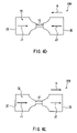
- FIG. 4D is a plan view to explain an operation of the magnetoresistance effect element according to Embodiment 2.
- FIG. 4E is a plan view to explain an operation of the magnetoresistance effect element according to Embodiment 2.
- FIG. 5A is a plan view showing a magnetic head according to Embodiment 3.
- FIG. 5B is a front view showing a magnetic head according to Embodiment 3.
- FIG. 6 is a front view showing a recording/reproducing apparatus according to Embodiment 4.
- FIG. 7A is a plan view showing a first memory element according to Embodiment 5.
- FIG. 7B is a front view showing a first memory element according to Embodiment 5.
- FIG. 7C is a plan view to explain an operation of the first memory element according to Embodiment 5.
- FIG. 8A is a plan view showing a second memory element according to Embodiment 5.
- FIG. 8B is a plan view to explain an operation of the second memory element according to Embodiment 5.
- FIG. 9 is a perspective view showing a memory array according to Embodiment 5.
- FIG. 10 is a perspective view showing a magnetoresistance effect element according to Embodiment 6.
- FIG. 11 is a perspective view to explain a method for manufacturing a magnetoresistance effect element according to Embodiment 6.
- FIG. 12A is a perspective view to explain an electronic device according to Embodiment 6.
- FIG. 12B is a perspective view to explain a method for manufacturing an electronic device according to Embodiment 6.
- FIG. 13A is a plan view to explain a method for manufacturing another electronic device according to Embodiment 6.
- FIG. 13B is a plan view to explain a method for manufacturing another electronic device according to Embodiment 6.
- FIG. 13C is a plan view to explain a method for manufacturing another electronic device according to Embodiment 6.
- FIG. 1A is a plan view showing an electronic device 100 according to Embodiment 1 ;
- FIG. 1B is a cross-sectional view taken along a line 1 B- 1 B in FIG. 1A ; and
- FIG. 1C is a cross-sectional view taken along a line 1 C- 1 C in FIG. 1B .
- the electronic device 100 has rectangular parallelepiped shaped electrodes 2 and 3 formed on a substrate 8 .
- the electrodes 2 and 3 have opposing surfaces 5 and 6 that are opposed to each other, respectively.
- Materials for the electrodes 2 and 3 are desirably metal or alloy.
- the electronic device 100 is provided with a cylindrical support 4 including a carbon nano-tube for bridging the opposing surface 5 of the electrode 2 and the opposing surface 6 of the electrode 3 .
- the carbon nano-tube may be a single layer carbon nano-tube (SWCNT) or may be a multiple layer carbon nano-tube (MWCNT).
- the electronic device 100 has a metal conductor thin film 7 that is electrically connected to the electrodes 2 and 3 .
- the metal conductor thin film 7 includes a metal conductor portion 1 .
- the metal conductor portion 1 bridges a gap between the electrodes 2 and 3 along the support 4 .
- the bridge length L of the metal conductor portion 1 is not more than a mean free path ⁇ of electrons in the metal conductor portion 1 at the operation temperature of the electronic device 100 .
- the value of the mean free path ⁇ of electrons in the metal conductor portion 1 is different depending upon the operation temperature of the electronic device 100 and the materials of the metal conductor portion 1 that is actually used for the electronic device.
- the value of the mean free path ⁇ of electrons is 100 nm or more.
- the value is on the order of about 10 nm.
- the material of the metal conductor portion 1 includes impurities, the value of the mean free path ⁇ of electrons in the metal conductor portion 1 is shorter than that of the mean free path for pure materials. Therefore, the bridge length L of the metal conductor portion 1 is in the range from, for example, 1 nm to 1000 nm in accordance with the chemical composition of the metal conductor portion 1 .
- the operation temperature of the electronic device 100 is 4.2 K or more and 523 K or less. Furthermore, from the viewpoint that a coolant for the electronic device 100 can be liquid N 2 instead of liquid He and that the manufacturing cost and running cost can be reduced, the operation temperature is preferably 77 K or more and 523 K or less. Furthermore, when an apparatus combining the electronic device 100 according to this Embodiment and other electronic devices (for example, semiconductor device, magnetic medium, etc.), if it is necessary to consider the operation temperature of the electronic devices other than the electronic device 100 of the Embodiment, the operation temperature may be 273 K or more and 523 K or less.
- FIGS. 1D and 1E are cross sectional views to explain the method for manufacturing the electronic device 100 .
- the electrodes 2 and 3 are formed on the substrate 8 with a gap having the bridge length L therebetween.
- a catalyst 9 for promoting a formation reaction of a carbon nano-tube is provided on the electrodes 2 and 3 .
- the carbon nano-tube is allowed to grow from each catalyst 9 by, for example, a chemical vapor deposition method so as to bridge between the electrodes 2 and 3 , and thus a support 4 is formed.
- a metal conductor thin film 7 is deposited by, for example, a vapor deposition method, and thereby the metal conductive portion 1 is formed along the support 4 so as to complete an electronic device 100 shown in FIGS. 1A to 1C .
- the electronic device 100 provided with a metal conductor portion 1 having not more than the bridge length L of the mean free path ⁇ of electron can be manufactured.
- the metal conductor portion 1 is responsible for electrical conduction between the electrodes 2 and 3 .
- This metal conductor portion 1 is formed of metal. Therefore, unlike the carbon nano-tube of non-patent document 4 that is not capable of controlling the conductivity, the metal conductor portion 1 has a stable conductivity.
- the metal conductor thin film 7 including a metal conductor portion 1 is formed of metal, unlike the carbon nano-tube of non-patent document 4, contact resistance between the electrodes 2 and 3 becomes extremely small. Therefore, the electric property is stable, and a problem of a large contact resistance generated between the carbon nano-tube and the electrodes can be solved.
- FIG. 2A is a cross-sectional view showing an electronic device 100 to explain a method for measuring the bridge length L of the metal conductor portion
- FIG. 2B is a front view to explain a method for measuring the bridge length L
- FIG. 2C is a graph for measuring a bridge length L.
- bridge length L of a metal conductor portion denotes a length along the central axis from a point P 1 in which a cross-sectional area along the central axis of the electronic device rapidly is decreased to a point P 2 in which a cross-sectional area of the electronic device rapidly is increased.
- a plurality of electronic devices 100 of the same standard that are manufactured under the same conditions and have the same shape and size are prepared. It can be confirmed whether or not the shape and size of the metal conductor portions 1 of the plurality of electronic devices 100 are the same by an analysis technology such as photography by using TEM (transmission electron microscope).
- the electronic device 100 is cut by using a STM (Scanning Tunneling Microscope) or a three-dimensional TEM so that a cross section simultaneously containing a metal conductor portion 1 and a metal conductor thin film 7 on the electrodes 2 and 3 can be obtained.
- FIG. 2A shows one example of the cross sectional shape obtained by this cutting.
- a central axis X of the metal conductor portion 1 is determined.
- the central axis X is determined in accordance with the cross sectional shape of the metal conductor portion 1 .
- a cross sectional shape of the metal conductor portion 1 is rectangular, and the central axis X is a straight line connecting the middle point of the side of the rectangular at the side of the electrode 2 and the middle point of the side at the side of the electrode 3 .
- a cross sectional area S of the electronic device 100 along the cross section perpendicular to the central axis X is determined along the central axis X.
- the electronic device 100 is cut by using, for example SIM.
- the shape is analyzed by photomicrography such as STM, three dimensional TEM, and the like, or by analyzing technology of image data, etc., the cross sectional area S of the cross section obtained by cutting.
- data of the cross sectional area S is determined along the central axis X and forms a graph shown in FIG. 2C in which a central axis X is shown in a lateral axis and a cross sectional area S is shown in a longitudinal axis.
- a point P 1 in which a cross sectional area S rapidly is decreased along a central axis X and a point P 2 in which a cross sectional area S rapidly is increased are determined.
- the sectional area of electrode 2 is not included in sectional area S, resulting in that sectional area S decreases rapidly at a point P 1 .
- the sectional area of electrode 3 is included in sectional area S, resulting in that sectional area S increases rapidly at a point P 2 .
- the length between the point P 1 and the point P 2 along the central axis X is defined as a bridge length of the metal conductor portion 1 .
- FIG. 2D is a cross-sectional view showing another electronic device 100 P to explain a method for measuring a bridge length L of a metal conductor portion;
- FIG. 2E is a front view thereof, and
- FIG. 2F is another graph for measuring a bridge length L.
- a contour of the electrodes 2 P and 3 P of the electronic device 100 P, a metal conductor thin film 7 P and a metal conductor portion 1 P includes a curved line unlike the example shown in FIGS. 2A to 2C .
- a central axis X is determined; a cross sectional area S is determined along the central axis X; and a graph of a cross sectional area S shown in FIG. 2F is formed. Then, a point P 1 in which a cross sectional area S is decreased rapidly along the central axis X and a point P 2 in which a cross sectional area S is increased rapidly are determined.
- the length between the point P 1 and the point P 2 along the central axis X is defined as a bridge length L of the metal conductor portion 1 .
- a contour of the cross section of the metal conductor portion 1 P and the metal conductor thin film 7 P includes a curved line, however, since a point P 1 in which a cross sectional area S is decreased rapidly and a point P 2 in which a cross sectional area S is increased rapidly appear in a graph similar to the example shown in FIG. 2A to 2C , the bridge length L between the point P 1 and the point P 2 along the central axis X can be measured.
- FIGS. 2I to 2U are views showing various cross sectional shapes and central axes X of the metal conductor portion 1 .
- the cross section of the metal conductor portion 1 can be formed in various shapes as shown in FIGS. 2I to 2U .
- the central axis X is defined in accordance with the cross sectional shape of the metal conductor portion as mentioned above.
- a left side of the paper shows the side of the electrode 2 and a right side of the paper shows the side of the electrode 3 .
- the metal conductor portion has a shape having two bottom surfaces and a cylindrical side surface formed between these two bottom surfaces. Then, the cross sectional shape of the metal conductor portion in this Embodiment can satisfy any of the following conditions [a] to [g].
- lines (two lines in the longitudinal direction) showing the periphery of the metal conductor portion is any of the following [a] to [g].
- FIGS. 2I to 2U show examples of cross sectional shapes showing only the metal conductor portion 1 satisfying the above-mentioned conditions [a] to [g].
- the cross sectional shape of the metal conductor portion 1 shown in FIG. 2I corresponds to the cross sectional shape of the metal conductor portion 1 mentioned with reference to FIGS. 1A to 1C and satisfies the condition [a].
- the cross sectional shape shown in FIG. 2J corresponds to the cross sectional shape of the metal conductor portion 1 P mentioned with reference to FIGS. 2D and 2E and satisfies the condition [d].
- the cross sectional shape shown in FIG. 2K satisfies the condition [g].
- the cross sectional shape shown in FIG. 2L satisfies the condition [d].
- FIG. 2M satisfies the condition [f].
- FIGS. 2N and 20 satisfy the condition [c].
- FIGS. 2P and 2Q satisfy the condition [f].
- FIG. 2R satisfies the condition [c].
- FIGS. 2S and 2T satisfy the condition [d].
- FIG. 2U satisfies the condition [g].
- the shape of the bottom surface of the metal conductor portion in the Embodiment is not particularly limited. Furthermore, the shapes and the size of the two bottom surfaces (the surfaces at the side of the electrode 2 and the side of the electrode 3 ) may be the same as each other or may be different from each other. Furthermore, the side surface formed between the two bottom surfaces may be a flat or curved surface or combination of a flat surface and a curved surface.
- a cylindrical metal conductor portion in the embodiment has a shape satisfying all of the following conditions [h] to [l] simultaneously.
- a central axis of the metal conductor portion is a straight line
- Examples of the cylindrical metal conductor portion having the shape that satisfies the conditions [h] to [ 1 ] at the same time may include the metal conductor portions having the cross sectional shapes shown in FIGS. 2I and 2L .
- the central axis X of the metal conductor portion 1 is one straight line in general. However, the central axis X of the metal conductor portion 1 having the cross sectional shape shown in FIG. 2P is defined by the combination of two straight lines; and the central axis X of the metal conductor portion 1 having the cross sectional shape shown in FIG. 2R is defined by the combination of a straight line and a curved line.
- the central axes X of the metal conductor portion 1 having the cross sectional shape shown in FIGS. 2O , 2 S and 2 T are defined by a curved surface.
- At least one of a concave portion and a convex portion may be formed by a processing technique such as STM.
- STM processing technique
- the cross sectional shape of the metal conductor portion before the concave portion and the convex portion are formed (or a metal conductor portion provided that the concave portion and convex portion are not formed) has any of the above-mentioned shapes [a] to [g].
- the shape of the support 4 is not particularly limited as long as the above-mentioned metal conductor portion 1 can be formed.
- the bridge length L of the metal conductor portion 1 that is responsible for electrical conduction is not more than the mean free path ⁇ of electrons in the metal conductor portion 1 at the operation temperature of the electronic device. Therefore, a phenomenon occurs called a ballistic conduction capable of allowing electrons to pass through the metal conductor portion 1 without being scattered and a phenomenon occurs called a quantum conductance in which the conductivity (conductance) changes stepwise with respect to the cross sectional area of the metal conductor portion 1 .
- the size of the metal conductor portion is on the order of nanometers because the metal conductor portion is formed on the carbon nano-tube, and the ballistic conduction and the quantum conductance can be observed also at relatively high temperatures.
- a gate portion is provided in the vicinity of the metal conductor portion 1 and the electrodes 2 and 3 formed of a magnetic film are served as a source and a drain. Thereby, a spin transistor can be achieved. Furthermore, if the metal conductor portion 1 and the support 4 are separated from the electrodes 2 and 3 , a single electron transistor using the coulomb brocade phenomenon can be achieved.
- the bridge length L of the metal conductor portion 1 is a value that is not more than the larger of the value of the length of electron spin diffusion in the metal conductor portion at the operation temperature of the magnetoresistance effect element and the value of mean free path ⁇ of electron in the metal conductor portion at the operation temperature of the magnetoresistance effect element.
- the value of the length of electron spin diffusion is larger than the mean free path ⁇ of electron.
- the length of electron spin diffusion is about 50 nm and the mean free path ⁇ of electron is 5 nm. Therefore, the bridge length L of the metal conductor portion 1 generally may be set to the length of electron spin diffusion or less.
- the bridge length L may be set to not more than a mean free path ⁇ of electron. Note here that when a length of electron spin diffusion and a mean free path ⁇ of electron are equal to each other, the bridge length L may be set to the equal value or less.
- the catalyst 9 uses metal/alloy particles or film containing at least one atom selected from the group consisting of Fe, Co and Ni. It is thought that these catalysts promote the reaction in which carbon (C) generated by decomposing CH 4 , etc. grows into a carbon nano-tube when the carbon nano-tube is formed by a CVD method, etc.
- the support 4 made of carbon nano-tube may be removed.
- the support 4 may be selectively removed by oxygen asher.
- the support 4 may be removed by irradiating the support 4 with laser.
- the support 4 may remain.
- the substrate 8 may be removed.
- the CNT of the substrate 8 shows three kinds of properties of a conductor, a semiconductor and an insulator, by removing the substrate 8 composed of CNT, the electric property of the electronic device becomes more stable.
- FIG. 3A is a plan view showing a further electronic device 100 A according to Embodiment 1;
- FIG. 3B is a cross-sectional view taken along a line 3 B- 3 B of FIG. 3A ; and
- FIG. 3C is a cross-sectional view taken along a line 3 C- 3 C of FIG. 3B .
- the same components mentioned with reference to FIGS. 1A to 1E are denoted with the same reference numerals, and the repeated description may be omitted.
- the support may be formed on the surface of the both electrodes.
- the support 4 A of the electronic device 100 A is formed on the surface of the electrode 2 and on the surface of the electrode 3 . When seen from the direction perpendicular to the bottom surface of the electrodes 2 and 3 , the support 4 A bridges a gap between the electrodes 2 and 3 .
- the metal conductor thin film 7 A of the electronic device 100 A is formed on the electrodes 2 and 3 . When seen from the direction perpendicular to the bottom surface of the electrodes 2 and 3 , the metal conductor portion 7 A includes a metal conductor portion 1 A that bridges a gap between the electrodes 2 and 3 along the support 4 A.
- the bridge length L of the metal conductor portion 1 A is not longer than the mean free path ⁇ of electron in the metal conductor portion 1 A at the operation temperature of the electronic device 100 A.
- the thus configured electronic device 100 A has the same effect as that of the above-mentioned electronic device 100 .
- FIG. 3D is a plan view showing a further electronic device 100 B according to Embodiment 1;
- FIG. 3E is a cross-sectional view taken along a line 3 E- 3 E of FIG. 3D ; and
- FIG. 3F is a cross-sectional view taken along a line 3 F- 3 F of FIG. 3E .
- the same components mentioned with reference to FIGS. 1A to 1E are denoted with the same reference numerals, and the repeated description may be omitted.
- the electrode may have a triangular prism shape.
- the electronic device 100 B is provided with triangular prismatic electrodes 2 B and 3 B.
- the electrodes 2 B and 3 B are formed at the positions respectively so that apex of the surfaces thereof are opposed to each other when seen from the direction perpendicular to the bottom surface.
- the support 4 B of the electronic device 100 B bridges a gap between the triangular prismatic shaped electrodes 2 B and 3 B.
- the metal conductor thin film 7 B of the electronic device 100 B includes a metal conductor potion 1 B that bridges a gap between the electrodes 2 B and 3 B along the support 4 B seen from the direction perpendicular to the bottom surfaces.
- the length of the bridge of the metal conductor portion 1 B is not more than the mean free path of electron in the metal conductor portion 1 B.
- the thus configured electronic device 100 B also has the same effect as that of the above-mentioned electronic device 100 .
- FIG. 3G is a plan view showing a yet further electronic device 100 C according to Embodiment 1;
- FIG. 3H is a cross-sectional view taken along a line 3 H- 3 H of FIG. 3G ; and
- FIG. 3I is a cross-sectional view taken along a line 3 I- 3 I of FIG. 3H .
- the electrode may have a cylindrical shape.
- the electronic device 100 C has cylindrical shaped electrodes 2 C and 3 C.
- the support 4 C of the electronic device 100 C bridges a gap between the electrodes 2 C and 3 C.
- the electronic device 100 C has the metal conductor thin film 7 C including the metal conductor portion 1 C.
- the bridge length L of the metal conductor portion 1 C is not more than the mean free path ⁇ of electron in the metal conductor portion 1 C.
- the thus configured electronic device 100 C also has the same effect as that of the above-mentioned electronic device 100 .
- FIG. 3J is a plan view showing a further electronic device 100 D according to Embodiment 1;
- FIG. 3K is a cross-sectional view taken along a line 3 K- 3 K of FIG. 3J ; and
- FIG. 3L is a cross-sectional view taken along a line 3 L- 3 L of FIG. 3K
- the metal conductor for directly bridging the opposing surfaces of both electrodes may be formed.
- the electronic device 100 D includes a cylindrical support 4 made of carbon nano-tube that bridges between the opposing surface 5 of the electrode 2 and the opposing surface 6 of the electrode 3 ; and the metal conductor 1 D that directly bridges between the opposing surface 5 of the electrode 2 and the opposing surface 6 of the electrode 3 along the support 4 .
- a metal conductor thin film 7 D is formed separately from the metal conductor 1 D.
- the bridge length L of the metal conductor 1 D is not more than the mean free path ⁇ of electron in the metal conductor portion 1 D.
- the thus configured electronic device 100 D has the same effect as that of the above-mentioned electronic device 100 .
- FIG. 4A is a plan view showing a magnetoresistance effect element 200 according to Embodiment 2 ;
- FIG. 4B is a front view thereof, and
- FIG. 4C is a cross-sectional view taken along a line 4 C- 4 C of FIG. 4B .
- the same components as those mentioned in Embodiment 1 are denoted with the same reference numerals, and the repeated description may be omitted.
- the magnetoresistance effect element 200 includes electrodes 2 E and 3 E made of a magnetic substance.
- the electrodes 2 E and 3 E respectively have the opposing surfaces 5 E and 6 E opposing each other.
- the electrodes 2 E and 3 E include a curved portion having a width D that is reduced to the width d respectively toward the opposing surfaces 5 E and 6 E.
- the magnetoresistance effect element 200 is provided with a cylindrical support 4 E made of a carbon nano-tube that bridges the opposing surface 5 E of the electrode 2 E and the opposing surface 6 E of the electrode 3 E.
- the magnetoresistance effect element 200 has a metal conductor thin film 7 E electrically connected to the electrodes 2 E and 3 E. It is preferable that the metal conductor thin film 7 E includes a magnetic substance.
- the metal conductor thin film 7 E includes the metal conductor portion 1 E.
- the metal conductor portion 1 E bridges a gap between the electrodes 2 E and 3 E along the support 4 E seen from the direction perpendicular to the bottom surface of the electrodes 2 E and 3 E.
- the bridge length L of the metal conductor portion 1 E is not more than a value that is the larger of the value of the length of electron spin diffusion in the metal conductor portion 1 E at the operation temperature of the magnetoresistance effect element 200 and the value of mean free path ⁇ of electron in the metal conductor portion 1 E at the operation temperature of the magnetoresistance effect element 200 .
- the cross sectional area S 1 of the electrode 2 E, the cross sectional area S 2 of the electrode 3 E and the cross sectional area S 3 of the metal conductor portion 1 E satisfy the relationship: S 3 ⁇ S 1 and S 3 ⁇ S 2 .
- the cross sectional area S 3 of the metal conductor portion is set to be smaller than the cross sectional areas Si and S 2 of the electrodes, when the metal conductor portion 1 E is made of a magnetic substance, a magnetic domain wall can be pinned in the metal conductor portion 1 E easily. Furthermore, also in the case where the metal conductor portion 1 E is not made of a magnetic substance, when the cross sectional area S 3 of the metal conductor portion is set to be smaller than the cross sectional areas S 1 and S 2 of the electrode, a main portion of the resistance of the magnetic resistance element is allowed to be carried out by the metal conductor portion 1 E.
- the cross-sectional areas S 1 , S 2 and S 3 are cross-sectional areas along the cross section that is perpendicular to the central axis of the metal conductor portion used for determining the bridge length L mentioned in Embodiment 1.
- electrodes 2 E and 3 E including a magnetic substance are formed on a substrate 8 with a gap having the bridge length L therebetween.
- a catalyst for promoting a formation reaction of a carbon nano-tube is provided on the electrodes 2 E and 3 E.
- the carbon nano-tube is allowed to grow from each catalyst 9 by, for example, a chemical vapor deposition (CVD) method so as to bridge between the electrodes 2 E and 3 E, and thus a support 4 E is formed.
- CVD chemical vapor deposition
- a metal conductor thin film 7 E is deposited by, for example, a vapor deposition method, and thereby forms the metal conductive portion 1 E so as to complete an magnetoresistance effect element 200 .
- the metal conductor thin film 7 E By depositing the metal conductor thin film 7 E on the support 4 E of the carbon nano-tube, it is possible to form the metal conductor portion 1 E having the bridge length L that is not more than a value that is the larger of the value of the length of electron spin diffusion and the value of mean free path ⁇ of electron.
- This metal conductor portion 1 E is responsible for electrical conduction between the electrodes 2 E and 3 E.
- This metal conductor portion 1 E is made of metal. Therefore, unlike the carbon nano-tube of non-patent document 1 that is not capable of controlling the conductivity, the metal conductor portion 1 E has a stable conductivity. Furthermore, since the metal conductor thin film 7 including a metal conductor portion 1 E is formed of metal, unlike the carbon nano-tube of non-patent document 4, contact resistance between the electrodes 2 E and 3 E becomes extremely small. Therefore, the electric property is stable, and a problem of a large contact resistance generated between the carbon nano-tube and the electrodes can be solved.
- a phenomenon called a ballistic conduction capable of allowing electrons to pass through the metal conductor portion 1 E without being scattered is observed.
- the magnetization direction of the electrodes 2 E and 3 E can be controlled, and a magnetoresistance effect element having an extremely high MR ratio can be obtained owing to the ballistic conduction.
- FIGS. 4D and 4E are plan views to explain an operation of the magnetoresistance effect element 200 when a magnetic substance is used for the metal conductor portion 1 E.
- FIG. 4D when the magnetization direction J 2 of the electrode 3 E is in anti-parallel to the magnetization direction J 1 of the electrode 2 E due to the external magnetic field H, since the magnetic domain wall is pined to the metal conductor portion 1 E, electrons are scattered by the magnetic domain wall and resistance becomes high.
- FIG. 4D when the magnetization direction J 2 of the electrode 3 E is in anti-parallel to the magnetization direction J 1 of the electrode 2 E due to the external magnetic field H, since the magnetic domain wall is pined to the metal conductor portion 1 E, electrons are scattered by the magnetic domain wall and resistance becomes high.
- FIG. 4D when the magnetization direction J 2 of the electrode 3 E is in anti-parallel to the magnetization direction J 1 of the electrode 2 E due to the external magnetic field H, since the magnetic domain wall is pined to the metal conductor portion 1 E,
- the metal conductor portion 1 E having the length of a bridge that is not more than the larger of the length of electron spin diffusion and the mean free path ⁇ of electrons since a ballistic conduction capable of allowing electrons to pass through the metal conductor portion 1 E without being scattered occurs, the difference between the resistance between the electrodes 2 E and 3 E in an anti-parallel state shown in FIG. 4D and the resistance between the electrodes 2 E and 3 E in a parallel state in FIG. 4E becomes extremely large.
- a magnetoresistance effect element having a MR ratio of 100% or more, that is, a much larger MR ratio than that of a conventional GMR element can be realized.
- a large MR tatio can be obtained by forming a concave portion in a metal conductor portion 1 E so as to trap a magnetic domain wall and to keep the resistance high and then by allowing electric current that shows a certain threshold value or more to flow from one of the electrodes 2 E and 3 E so as extinguish the magnetic domain wall and to lower the resistance.
- magnetic substances used for the electrodes 2 E and 3 E and the metal conductor portion 1 E are composed of a material containing at least one element selected from the group consisting of Fe, Co and Ni or a semi-metal magnetic material having a large spin polarizability.
- the catalyst contains at least one element selected from the group consisting of Fe, Co and Ni.
- FIG. 5A is a plan view showing a magnetic head 300 according to Embodiment 3 ; and FIG. 5B is a front view thereof.
- the same components mentioned in Embodiments 1 and 2 are denoted with the same reference numerals, and the repeated description may be omitted.
- the magnetic head 300 includes a magnetoresistance effect element 200 A.
- the magnetoresistance effect element 200 A includes the electrodes 2 F and 3 F composed of a magnetic substance.
- the electrodes 2 F and 3 F have the opposing surfaces 5 F and 6 F, respectively.
- the electrodes 2 F and 3 F include a curved portion having a width D that decreases toward the width d of the opposing surfaces 5 F and 6 F, respectively.
- the magnetoresistance effect element 200 A is provided with a cylindrical support 4 F made of carbon nano-tube that bridges between the opposing surface 5 F of the electrodes 2 F and the opposing surface 6 F of the electrodes 3 F
- the magnetoresistance effect element 200 A has a metal conductor thin film 7 F electrically connected to the electrodes 2 F and 3 F.
- the metal conductor thin film 7 F includes a metal conductor portion 1 F.
- the metal conductor portion 1 F bridges a gap between the electrodes 2 and 3 along the support 4 A seen from the direction perpendicular to the bottom surface of the electrodes 2 F and 3 F.
- the bridge length L of the metal conductor portion 1 F is not more than a value that is the larger of the value of the length of electron spin diffusion and the value of mean free path ⁇ of electron, in the metal conductor portion 1 F at the operation temperature of the magnetoresistance effect element 200 A.
- the magnetic head 300 includes lead wires 10 that are electrically connected to the electrodes 2 F and 3 F of the magnetoresistance effect element 200 A and applies voltage to both electrodes
- the electrode 3 F includes an insulating film 15 , a base film 16 that is made of Ta, etc. and formed on the insulating film 15 , and a free layer 11 that is formed on the base film 16 and has a magnetization direction J 2 rotating easily when the external magnetic field H is applied.
- the electrode 2 F includes an insulating film 33 , a base film 34 that is made of Ta, etc. and formed on the insulating film 34 , and a pinned layer 12 that is formed on the base film 34 and has a magnetization direction J 1 that does not easily rotate even if the external magnetic field H is applied.
- the pinned layer 12 includes an antiferromagnetic film 14 formed on the base film 34 and a magnetic film formed on the antiferromagnetic film 14 and pinned by the antiferromagnetic film 14 .
- electrodes 2 F and 3 F are formed on a substrate 8 with a gap having a length of bridge L therebetween.
- a lead wire 10 is connected to the electrodes 2 F and 3 F, respectively.
- a catalyst for promoting a formation reaction of a carbon nano-tube is provided on the electrodes 2 F and 3 F.
- the carbon nano-tube is allowed to grow from each catalyst by, for example, a chemical vapor deposition (CVD) method so as to bridge between the electrodes 2 F and 3 F, and thus a support 4 F is formed.
- CVD chemical vapor deposition
- a metal conductor thin film 7 F is deposited by, for example, a vapor deposition method, and thus the metal conductor portion 1 F is formed along the support 4 F.
- the metal conductor thin film 7 F By depositing the metal conductor thin film 7 F on the support 4 F of the carbon nano-tube, it is possible to form the metal conductor portion 1 F having the bridge length L having a value that is larger value one the value of the length of electron spin diffusion and the value of mean free path ⁇ of electron.
- This metal conductor portion 1 F is in charge of electrical conduction between the electrodes 2 F and 3 F.
- This metal conductor portion 1 F is made of metal. Therefore, unlike the carbon nano-tube of non-patent document 4 that is not capable of controlling the conductivity, the metal conductor portion 1 F has a stable conductivity. Furthermore, since the metal conductor thin film 7 F including a metal conductor portion IF is formed of metal, unlike the carbon nano-tube of non-patent document 4, contact resistance between the electrodes 2 F and 3 F becomes extremely small. Therefore, the electric property is stable, and a problem of a large contact resistance generated between the carbon nano-tube and the electrodes can be solved.
- a phenomenon called a ballistic conduction capable of allowing electrons to pass through the metal conductor portion 1 F without being scattered is observed.
- a magnetoresistance effect element having an extremely high MR ratio can be obtained.
- the pinned layer 12 is composed of the antiferromagnetic film 14 and a magnetic film pinned by the antiferromagnetic film 14 , a magnetic head having a thermally stable property can be obtained.
- the magnetic film is pinned with the antiferromagnetic film 14 in the example shown in FIG. 5B but it may contain a hard magnetic film having a large coercive force or a composite film of a hard magnetic film having a large magnetic force and a magnetic force. In this case, the antiferromagnetic film 14 is not necessary.
- the magnetization direction of the magnetic layer provided in the pinned layer 12 must be fixed in one direction.
- the size of the element is extremely fine, so that the magnetization direction of the magnetic layer is affected by thermal fluctuation and it becomes difficult to fix the magnetization direction. Therefore, in this Embodiment, by the use of the antiferromagnetic film 14 , the pinning of the magnetic film is carried out, and even if the size of element becomes fine, the magnetization direction of the magnetic layer is not affected by the thermal fluctuation.
- a magnetization easy axis 30 of the free layer 11 is arranged so as to be perpendicular to the direction of the external magnetic field H to be detected.
- linearity of the signal output of the magnetoresistance effect element 200 A is improved.
- One method for achieving this is providing permanent magnets on both sides of the free layer 11 and fixing the magnetization easy axis 30 of the free layer 11 so as to be perpendicular to the direction of the external magnetic field H to be detected by the bias magnetic field thereof.
- Another method for achieving this is pinning a part of the both ends of the free layer 11 by an antiferromagnetic film provided separately from the antiferromagnetic film 14 so that the magnetization easy axis 30 of the free layer 11 is made to be perpendicular to the direction of magnetic field H.
- the free layer 11 is composed of two magnetic films that are exchange-bonded in anti-parallel to each other with a non-magnetic film interposed therebetween.
- M 1 and M 2 the magnetizations of the two magnetic layers
- t 1 and t 2 the film thickness are denoted by t 1 and t 2 .
- magnetic film also may be composed of two magnetic films that are exchange bonded in anti-parallel to each other with a non-magnetic film interposed therebetween, thus improving the stability with respect to the thermal fluctuation.
- (M 1 X ⁇ t 1 X ⁇ M 2 X ⁇ t 2 X) may be zero wherein M 1 X and M 2 X represent magnetization of the two respective magnetic films; and t 1 X and t 2 X represent the film thickness.
- materials of the free layer 11 and the magnetic film 13 are metal/alloy containing Fe, Co and Ni as a main component. Specific examples of the materials include NiFe, CoFe and CoFeNi, etc.
- an alloy film containing at least one element selected from the group consisting of Pt, Pd and Ir, and Mn element as a main component, for example, PtMn, IrMn and PtPdMn, are desirably used.
- the insulating films 15 and 33 may be composed of, for example, SiO 2 .
- the insulating films 15 and 33 need not be formed. However, in the case where the insulating films 15 and 33 are formed, CNT can be grown smoothly.
- FIG. 6 is a front view showing a recording/reproducing apparatus 400 according to Embodiment 4.
- the recording/reproducing apparatus 400 includes a recording head portion 17 and a reproducing head portion 18 .
- the recording head portion 17 has a winding portion 31 .
- When electric current flows to the winding portion 31 a magnetic field is leaked from a recording gap G 1 , and with this leaked magnetic field, information is recorded in a magnetic recording medium 19 .
- the reproducing head portion 18 has two shield portions 32 including a magnetic substance, and a magnetic head 300 according to Embodiment 3 provided between the shield portions 32 .
- a reading gap G 2 between the shields portion 32 is set so as to be narrower than two times the bit length BL recorded in a magnetic recording medium 19 .
- the information recorded in the magnetic recording medium 19 is detected by the magnetoresistance effect element 200 A of the magnetic head 300 of Embodiment 3 and read out via lead wires 10 (see FIG. 5A ).
- the magnetic head 300 of the reproducing head portion 18 of Embodiment 4 includes a magnetoresistance effect element 200 A of Embodiment 3.
- the magnetoresistance effect element 200 A includes a metal conductor portion 1 F (see FIGS.5A and 5B ). Since the bridge length L of the metal conductor portion 1 F is a value that is no more than the larger of the value of the length of electron spin diffusion and the value of mean free path ⁇ of electron in the metal conductor portion, the ballistic conduction can be realized at the metal conductor portion 1 F.
- the magnetic head 300 of the reproducing head portion 18 since the MR ratio of 100% that is higher as compared with a conventional GMR element or TMR element, a recording/reproducing apparatus with super high density of more than 100 Gb/inch 2 can be realized.
- FIG. 7A is a plan view showing a first memory element 500 according to Embodiment 5 ;
- FIG. 7B is a front view thereof, and
- FIG. 7C is a plan view to explain an operation of the first memory element 500 according to Embodiment 5.
- the same components as those mentioned in Embodiments 1 to 4 are denoted with the same reference numerals, and the repeated description may be omitted.
- the memory element 500 includes a magnetoresistance effect element 200 A mentioned in Embodiment 3 with reference to FIGS. 5A and 5B .
- the magnetoresistance effect element 200 A includes an electrode 3 F including a free layer 11 in which the magnetization is rotated easily with respect to the external magnetic field H; an electrode 2 F including a pinned layer 12 in which the magnetization is not rotated easily with respect to the external magnetic field H; and a metal conductor thin film 7 F including a metal conductor portion 1 F.
- the pinned layer 12 , the free layer 11 and the metal conductor portion 1 F are composed of a magnetic substance.
- a phenomenon called a ballistic conduction capable of allowing electrons to pass through the metal conductor portion 1 F without being scattered is observed.
- a magnetoresistance effect element having an extremely high MR ratio can be obtained.
- the memory element 500 further includes a word line 20 for generating an external magnetic field H 1 or H 2 that inverts the magnetization direction J 2 of the free layer 11 based on any of the electric currents 21 A and 21 B; and a current supplier 22 for supplying the word line 20 with any of the electric currents 21 A and 21 B.
- the word line 20 when the current supplier 22 supplies the word line 20 with an electric current 21 A, the word line 20 generates an external magnetic field H 1 .
- the magnetization direction J 1 of the pinned layer 12 is not magnetization-rotated in the direction of the external magnetic field H 1 , but the magnetization direction J 2 of the free layer 11 is magnetization-rotated in the direction of the external magnetic field H 1 . Therefore, the magnetization direction J 2 of the free layer 11 is in anti-parallel to the magnetization direction J 1 of the pinned layer 12 .
- the word line 20 when the electric current supplier 22 supplies the word line 20 with an electric current 21 B flowing in the opposite direction to the electric current 21 A, the word line 20 generates an external magnetic field H 2 in the opposite direction to the external magnetic field H 1 . Then, the magnetization direction J 2 of the free layer 11 is rotated in the direction of the external magnetic field H 2 . Therefore, the magnetization direction J 2 of the free layer 11 becomes in parallel to the magnetization direction J 1 of the pinned layer 12 .
- the metal conductor portion 1 F When the metal conductor portion 1 F is composed of a non-magnetic substance, a magnetic domain wall is not generated in the metal conductor portion 1 F. However, when the magnetization directions of the electrodes 2 F and 3 F are in parallel to each other, the metal conductor portion 1 F shows the ballistic conduction; and when the magnetization directions of the electrodes 2 F and 3 F are in anti-parallel to each other, spin scattering occurred. Therefore, in accordance with whether the magnetization directions of the electrodes 2 F and 3 F are in parallel or anti-parallel to each other, the change in the magnetic resistance that is larger than that of the conventional GMR element can be obtained.
- the metal conductor portion 1 F having a bridge length L that is a value not more than a value that is the larger of the value of the length of electron spin diffusion and the value of mean free path ⁇ of electron a phenomenon called a ballistic conduction capable of allowing electrons to pass through the metal conductor portion 1 F without being scattered can be realized. Therefore, the difference between the resistance in anti-parallel state shown in FIG. 7A and the resistance in parallel state shown in FIG. 7C becomes extremely large. Therefore, an extremely high MR ratio as compared with the MR ratio of a conventional magnetoresistance effect element having a maximum MR ratio of about 60% can be realized.
- FIG. 8A is a plan view showing a second memory element 600 according to Embodiment 5.
- FIG. 8B is a plan view to explain an operation of the second memory element 600 .
- the memory element 600 includes a magnetoresistance effect element 200 A.
- a ballistic conduction capable of allowing electrons to pass through the metal conductor portion 1 F without being scattered is observed.
- a magnetoresistance effect element having an extremely high MR ratio can be obtained as compared with a conventional GMR element and TMR element.
- the memory element 600 is provided with an electric current supplier 25 .
- the electric current supplier 25 supplies the magnetoresistance effect element 200 A with an electric current 23 flowing from the electrode 2 F to the electrode 3 F in the metal conductor portion 1 F and an electric current 24 flowing from the electrode 3 F to the electrode 2 F in the metal conductor portion 1 E.
- the basic configuration in this embodiment is the same as in the memory element 500 shown in FIGS. 7A to 7C except that a word line is not provided.
- the metal conductor portion 1 F is a non-magnetic conductor
- the magnetization direction J 2 of the free layer of the electrode 3 F is in anti-parallel to the magnetization direction J 1 of the pinned layer of the electrode 2 F.
- FIG. 8B by allowing an electric current 24 to flow from the side of the electrode 3 F including the free layer, the magnetization direction J 2 of the free layer of the electrode 3 F is inversed and in the anti-parallel state with respect to the magnetization direction J 1 of the pinned layer of the electrode 2 F.
- the metal conductor portion 1 F is a magnetic substance
- by allowing an electric current to flow from the electrode 3 F or the electrode 2 F it is possible to pin the magnetic domain wall with respect to the metal conductor portion 1 F or to remove the magnetic domain wall from the metal conductor portion 1 F.
- the current density of the current 23 and 24 is at least 1 ⁇ 10 5 A/cm 2 or more and desirably 1 ⁇ 10 6 A/cm 2 or more for a stable operation.
- the metal conductor portion is formed on the CNT, it is possible to reduce the width of the metal conductor portion to be 1 to 10 nm easily. Therefore, it is possible to realize the above-mentioned current density even without allowing a large current to flow. It is preferable that the current density of the electric current 23 and 24 is 1 ⁇ 10 8 A/cm 2 or less. If the current density is more than the upper limit, the memory element may be destroyed during operation.
- the memory element 600 shown in FIGS. 8A and 8B do not need the word line, unlike the memory element 500 shown in FIGS. 7A to 7C .
- electric current of the word line necessary to the magnetization reversal was increased when the memory element became small, which was a serious problem.
- This memory element 600 is free from such a problem.
- the memory element 600 does not need a word line as mentioned above, it has a configuration that is simple and has a small size. Thus, it is possible to realize a memory element that has a simple and small-sized configuration in which cell area is small, space for installing the memory is small and recording density is high. According to the memory element 600 , an extremely high MR ratio as compared with the MR ratio of a conventional magnetoresistance effect element, in which the maximum MR ratio is about 60%.
- the pinned layer 11 of the memory element shown in FIGS. 7A to 7C , 8 A and 8 B may be pinned by using an antiferromagnetic film provided below or above the pinned layer 11 .
- this antiferromagnetic film contains at least one element selected from the group consisting of Pt, Pd and Ir and an alloy film containing Mn element as a main component, for example PtMn, IrMn and PtPdMn.
- FIG. 9 is a perspective view showing a memory array 700 according to Embodiment 5.
- the memory elements of this embodiment mentioned with reference to FIGS. 8A and 8B are arranged in a matrix so as to make a memory element having a configuration capable of recording information on individual memory elements and reading out information from the individual memory elements.
- a memory array whose density is higher than 1 Gb.
- the magnetoresistance effect elements 200 A are arranged in a matrix (m row ⁇ n column).
- M conductor lines X 1 , X 2 , . . . , X (m ⁇ 1), Xm are provided.
- Connecting lines CL (i, j) (1 ⁇ i ⁇ m and 1 ⁇ j ⁇ n) for connecting the electrode 3 F of each magnetoresistance effect element 200 A and m conductive lines X 1 , X 2 , . . . , X (m ⁇ 1), Xm are provided in a matrix.
- n conductive lines Y 1 , Y 2 , . . . , Y (n ⁇ 1), Yn connected to the electrodes 2 F of the magnetoresistance effect elements 200 A arranged in the direction of row are provided.
- the memory array 700 includes a write unit 35 .
- the write unit 35 writes information independently on the magnetoresistance effect element 200 A via the conductive line and the connecting line by inversing the direction of the electric current flowing in the metal conductor portion 1 F of the magnetoresistance effect element 200 A so as to change the magnetization direction of the electrodes 2 F and 3 F in parallel or in anti-parallel.
- the memory array 700 includes a read unit 36 .
- the read unit 36 reads information written in the magnetoresistance effect element 200 A independently by measuring the resistance value between the electrodes 2 F and 3 F of the magnetoresistance effect element 200 A that are different in accordance with the magnetization direction of the electrodes 2 F and 3 F.
- Information recording can be carried out by allowing a relatively large current to flow to the conductive line Xi, the connecting line CL (i, j), and the conductive line Yj. At this time, depending upon whether the direction in which the electric current is allowed to flow is from the side of the conductive line Xi or from the side of the conductive line Yj, the magnetization direction of the electrodes 2 F and 3 F become in a parallel state or in an anti-parallel state.
- the metal conductor portion 1 F in the case of an anti-parallel state, a magnetic domain wall is pinned to the metal conductor portion and resistance becomes high; and in the case of a parallel state, a magnetic domain wall is removed from the metal conductor portion 1 F and the resistance becomes low.
- the metal conductor portion 1 F is composed of a non-magnetic substance, a magnetic domain wall is not provided in the metal conductor portion 1 E
- the metal conductor portion 1 F shows a ballistic conduction and the resistance becomes low; and when the magnetization directions are in anti-parallel to each other, the spin diffusion occurs and the resistance becomes high.
- the resistance between both electrodes 2 F and 3 F is measured and the written information can be read out in accordance with whether the measurement resistance value is high or low.
- the metal conductor portion 1 F is made of metal. Therefore, unlike the carbon nano-tube of non-patent document 4 that is not capable of controlling the conductivity, the metal conductor portion 1 F has a stable conductivity. Since the metal conductor thin film including the metal conductor portion 1 F is made of metal, unlike the carbon nano-tube of non-patent document 4, contacting resistance between the electrode 2 F and the electrode 3 F is extremely small. Therefore, the electric property is stabilized and the problem of contact resistance occurred between the carbon nano-tube and the electrode is solved.
- the bridge length L of the metal conductor portion 1 F is not more than a value that is the larger of the value of the length of electron spin diffusion and the value of mean free path ⁇ of electron, in the metal conductor portion 1 F, a phenomenon called a ballistic conduction capable of allowing electrons to pass through the metal conductor portion 1 F without being scattered is observed.
- a magnetoresistance effect element BMR (ballistic MR)
- BMR magnetoresistance effect element
- FIG. 10 is a perspective view showing a magnetoresistance effect element 800 according to Embodiment 6; and FIG. 11 is a perspective view to explain a method for manufacturing a magnetoresistance effect element 800 according to Embodiment 6.
- the magnetoresistance effect element 800 includes a pinned layer (first electrode film) PL that is not easily magnetization-rotated with respect to an external magnetic field.
- the pinned layer PL includes an antiferromagnetic film AF and a magnetic film ML formed on the antiferromagnetic film AF and pinned by the antiferromagnetic film AF.
- On the magnetic film ML a non-magnetic insulating film NL is formed.
- a free layer (second electrode film) FL that is magnetization rotated with respect to the external magnetic filed easily is formed.
- the free layer FL is composed of a magnetic film.
- the magnetoresistance effect element 800 includes a cylindrical shaped metal conductor C that penetrates the non-insulating film NL and connects the magnetic film ML and the free layer FL electrically.
- the metal conductor C is composed of a magnetic substance or nonmagnetic substance.
- the length L of the metal conductor C from the magnetic film Ml through the free layer FL is not more than the mean free path ⁇ of electrons of the metal conductor C at an operation temperature of the magnetoresistance effect element 800 .
- a method for manufacturing the thus configured magnetoresistance effect element 800 will be described. Firstly, the antiferromagnetic film AF and the magnetic film ML are formed on the substrate 8 in this order. Then, the non-magnetic insulating film NL is formed on the magnetic film ML to the thickness of the length L of the metal conductor C.
- a through hole 27 that reaches a magnetic film ML is formed by irradiating with field emission electron beams from a probe 26 of a scanning tunneling microscope (STM) including a carbon nano-tube. Then, the through hole 27 is filled with a metal conductor C. Then, a free layer FL is formed on the non-magnetic insulating film NL and a metal conductor C.
- STM scanning tunneling microscope
- the probe 26 of SIM for irradiating with field emission electron beam is formed of a carbon nano-tube, and fine and precise processing can be carried out securely. Therefore, the through hole 27 having fine size and shape of 1 nm to 1000 nm and in particular 1 nm to 100 nm can be formed. Thus, it is possible to obtain a metal conductor C that is filled with the magnetic substance so as to have a fine size and shape.
- a phenomenon called a ballistic conduction capable of allowing electrons to pass through the metal conductor C without being scattered and a phenomenon called a quantum conductance in which the conductivity changes stepwise with respect to the cross sectional area of the metal conductor C are observed.
- a magnetic domain wall is pinned on the metal conductor C made of a magnetic substance, thus increasing the resistance between the free layer FL and the pinned layer PL.
- the magnetic domain wall disappears from the metal conductor C, and thereby the resistance between the free layer FL and the pinned layer PL is decreased.
- a non-magnetic substance is used for the metal conductor C, a magnetic domain wall is not generated in the metal conductor portion.
- the magnetoresistance effect element 800 By changing the magnitude of the external magnetic field so as to cause the magnetization rotation of the free layer FL, the difference in angle between the fixed magnetization direction J 1 of the pinned layer PL and the magnetization direction J 2 of the free layer FL that is magnetization-rotated is changed and therefore, the resistance between the free layer FL and the pinned layer PL is changed.
- a magnetic head for detecting signals from the magnetic medium can be configured.
- magnetoresistance effect element 200 A arranged in a matrix shown in FIG. 9 is replaced by the magnetoresistance effect element 800 , a large capacitance memory array can be realized. This is because the use of the magnetoresistance effect element 800 , which allows an electric current to flow perpendicular to the film surface, can make a generally higher density than the magnetoresistance effect element 200 A, which allows an electric current to flow in parallel to the film surface.
- the quantum conductance By using the quantum conductance, by controlling the cross sectional area of the metal conductor C, it is possible to obtain an electronic device free from variation in conductivity in mass production generated in the case where the conductivity with respect to the cross sectional area is changed linearly.
- a semiconductor film having relatively high electric resistance in which electric current flows only in the metal conductor C when an electric current flows to the magnetoresistance effect element 800 , may be used instead of the non-magnetic insulating film NL.
- FIG. 12A is a perspective view to explain an electronic device 900 according to Embodiment 6.
- FIG. 12B is a perspective view to explain a method for manufacturing an electronic device 900 .
- the electronic device 900 includes electrodes 2 G and 3 G formed on the substrate 8 ; and an insulating film 28 formed in contact with the electrodes 2 G and 3 G between the electrodes 2 G and 3 G.
- a groove 29 that reaches from the electrode 2 G to the electrode 3 G is formed on the insulating film 28 .
- the groove 29 is filled with a metal conductor 1 G that is brought into contact with the electrodes 2 G and 3 G.
- the length L of the metal conductor 1 G is not more than the mean free path ⁇ of electron in the metal conductor 1 G at the operation temperature of the electronic device 900 .
- the method for manufacturing the thus configured electronic device 900 will be described. Firstly, the electrodes 2 G and 3 G disposed with a gap of the length L therebetween and the insulating film 28 are formed on the substrate 8 . Then, the groove 29 is formed that reaches from the electrode 2 G to the electrode 3 G is formed on the insulating film 28 by irradiating the field emission electron beam while moving the probe 26 of STM including the carbon nano-tube. Then, the groove 29 is filled with the metal conductor 1 G.
- the probe 26 of STM for irradiating with field emission electron beam is formed of a carbon nano-tube, fine and precise processing can be carried out securely. Therefore, the groove 29 having fine size and shape controlled in the order of 1 nm to 1000 nm and in particular 1 nm to 100 nm can be formed. Thus, it is possible to obtain a metal conductor 1 G that is filled with the magnetic substance in a fine size and shape.
- the metal conductor 1 G having the length L of not more than the mean free path ⁇ of electron a quantum conductance and a ballistic conduction are observed.
- the quantum conductance By using the quantum conductance, by controlling the cross sectional area of the metal conductor portion 1 G, an electronic device is free from variation in conductivity in mass production occurred in the case where the conductivity with respect to the cross sectional area is changed linearly.
- the ballistic conduction by controlling the magnetization directions of the electrodes 2 G and 3 G, a magnetoresistance effect element having an extremely high MR ratio and a magnetic head, a recording/reproducing apparatus, a memory element, a memory array using the magnetoresistance effect element can be obtained.
- the metal conductor 1 G may be provided with a concave portion.
- the concave portion of the metal conductor is a portion in which the cross sectional area along the cross section perpendicular to the direction of the length L of the metal conductor is smaller than that of the other portion.
- a groove 39 is formed substantially in the center of the insulating film 28 by irradiating the insulating film 28 with field emission electron beams while moving the probe of STM in the direction from the side of the electrode 2 G toward an arrow 38 ; and then a groove 41 is formed on the insulating film 28 by irradiating the insulating film 28 with field emission electron beams while moving the probe 26 of STM in the direction from the side of the electrode 3 G toward an arrow 40 so as to allow the tip of the groove 41 to reach the tip of the groove 39 .
- a groove 29 A having a convex portion 37 as shown in FIG. 13B is formed.
- the groove 29 A is filled with the metal conductor 1 G so as to form a metal conductor 1 G having a concave portion 37 A.
- the concave portion 37 A when the electronic device is used for the magnetoresistance effect element, if the magnetic substance is used for the metal conductor 1 G, the magnetic domain wall can be pinned on the site of the convex portion 37 A of the metal conductor 1 G securely.
- a SiO 2 layer On a Si substrate, a SiO 2 layer was provided. On the SiO 2 layer, a pair of electrodes made of Mo/Au were formed with an interval of 50 nm by sputtering and EB lithography. Then, a catalyst containing fine particles of Ni having a diameter of about 5 nm was applied on the electrodes. Then, CNT having a length of 50 nm and a diameter of about 1 nm was grown in the lateral direction by a CVD method using CH 4 at 800° C. so as to bridge between the both electrodes and form a support. On the CNT and both electrodes, an Au film was deposited to the thickness of 1 nm so as to form a metal conductor portion on the CNT and thus an electronic device was formed.
- a SiO 2 layer On a Si substrate, a SiO 2 layer was provided. On the SiO 2 layer, an electrode made of Ta/NiFe/CoFe and an electrode made of Ta/PtMn/CoFe were formed with an interval of 10 nm by sputtering and EB lithography. Then, a Co thin film, which serves as a catalyst, having a thickness of 0.5 nm was deposited on these electrodes. Then, CNT having a length of 10 nm and a diameter of about 20 nm was grown in the lateral direction by a CVD method using CH 4 at 400° C. so as to bridge between the both electrodes and form a support.
- a Co film was deposited to the thickness of 3 nm so as to form a metal conductor portion on the CNT and thus a magnetoresistance effect element 200 A shown in FIGS. 5A and 5B was formed.
- the magnetoresistance effect element was formed so that the maximum width of the both electrodes was set to 120 nm and the width was decreased toward the metal conductor portion.
- Lead wires were connected to these electrodes and thus a magnetic head 300 shown in FIGS. 5A and 5B was prepared.
- a certain voltage was applied and an external magnetic field was varied from 1 kOe to ⁇ 1 kOe, it was shown that the MR ratio was about 500%.
- a reproducing head portion having a reproducing track width of 120 nm was prepared.
- a recording/reproducing apparatus having a recording head portion and reproducing head portion shown in FIG. 6 was prepared.
- As the magnetic recording medium CoCrPt—SiO 2 based perpendicular magnetic recording medium was used. It was shown that information recorded on the magnetic recording medium with recording density of 200 Gb/inch 2 was able to be reproduced from this reproducing head portion at the operation temperature of 300 K
- a SiO 2 layer On a Si substrate, a SiO 2 layer was provided. On the SiO 2 layer, an electrode made of Ta/NiFe/CoFe and an electrode made of Ta/PtMn/CoFe were formed with an interval of 15 nm by sputtering and EB lithography. Then, a Co thin film, which serves as a catalyst, having a thickness of 0.5 nm was deposited on these electrodes. Then, CNT having a length of 15 nm and a diameter of about 6 nm was grown in the lateral direction by a CVD method using CH 4 at 450° C. so as to bridge between the both electrodes and form a support.
- a Co film was deposited to the thickness of 3 nm so as to form a metal conductor portion on the CNT and thus a magnetoresistance effect element 200 A shown in FIGS. 5A and 5B was formed.
- the magnetoresistance effect element was formed so that the maximum width of the both electrodes was set to 80 nm and the width was decreased toward the metal conductor portion.
- Lead wires were connected to these electrodes and thus a magnetic head 300 shown in FIGS. 5A and 5B was prepared.
- a certain voltage was applied and an external magnetic field was varied from 1 kOe to ⁇ 1 kOe, it was shown that the MR ratio was about 1000%.
- an electrode made of Ta/NiFe/CoFe and an electrode made of Ta/PtMn/CoFe were formed with an interval of 50 nm by sputtering. Then, a Co thin film having a thickness of 0.5 nm was deposited on these electrodes. Then, CNT having a length of 50 nm and a diameter of about 20 nm was grown in the lateral direction by a CVD method using CH 4 at 450° C. so as to bridge between the both electrodes and form a support. Note here that the film thickness of both electrodes is made about 20 nm.
- a 10 nm thick Cu film was deposited so as to form a metal conductor portion on the CNT and thus a magnetoresistance effect element 200 A as shown in FIGS. 5A and 5B was prepared.
- the magnetoresistance effect element 200 A was prepared so that the maximum width of the both electrodes was set to 200 nm and the width was decreased toward the metal conductor portion. Lead wires were connected to these electrodes and thus a magnetic head was prepared. When, at the operation temperature of 77 K, a certain voltage was applied and an external magnetic field was varied from 1 kOe to ⁇ 1 kOe, it was shown that the MR ratio was about 100%.
- a reproducing head portion having a reproducing track width of 200 nm was prepared.
- a recording/reproducing apparatus having a reproducing head portion and the recording head portion shown in FIG. 6 was prepared.
- As a magnetic recording medium CoCrPt—SiO 2 based perpendicular magnetic recording medium was used. It was shown that information recorded on the magnetic recording medium with a recording density of 120 Gb/inch 2 was able to be reproduced from this reproducing head portion at the operation temperature of 300 K.
- the memory element 600 shown in FIGS. 8A and 8B was prepared by using the magnetoresistance effect element 200 A shown in FIGS. 5A and 5B prepared in Example 4.
- the density of electric current flowing in the metal conductor portion was about 1 ⁇ 10 7 A/cm 2 and by allowing an electric current 23 to flow from the side of the electrode 2 F having a pinned layer as shown in FIG. 8A or by flowing current 24 from the side of the electrode 3 F having a free layer as shown in FIG. 8B , information of “1” or “0” is written.
- the magnetoresistance effect element 200 A of the memory element 600 prepared in Example 7 is arranged in a matrix as shown in FIG. 9 so as to prepare a large capacity of memory array 700 .
- the operation temperature of 300 K by appropriately selecting one of the m row ⁇ n column of magnetoresistance effect element 200 A, by making the density of electric current flowing in the conductive line and the connecting line be about 1 ⁇ 10 7 A/cm 2 and by flowing current from the side of the electrode 2 F of the magnetoresistance effect element 200 A or from the side of the electrode 3 F thereof, information of “1” or “0” is written in the selected magnetoresistance effect element 200 A.
- Ta base film was formed by sputtering, an antiferromagnetic film AF made of PtMn and a magnetic film ML made of CoFe were formed so as to prepare the pinned layer PL. Then, on the magnetic film ML, an Al film was formed by sputtering, and with natural oxidizing thereof, so a non-magnetic insulating film NL that is an Al 2 O 3 oxide film having a thickness of 3 nm was prepared.
- a fine hole having a diameter of 5 nm is formed by irradiating with field emission electron beam from a probe of a STM including a carbon nano-tube.
- a CoFe film was formed thereon by sputtering to form a free layer FL and at the same time, the hole formed on the above-mentioned Al 2 O 3 oxide film was filled with CoFe to form a metal conductor C.
- the free layer FL and the pinned layer PL thus were electrically connected to each other.
- This element was patterned to the width of 80 nm by EB lithography to prepare the magnetoresistance effect element 800 shown in FIG. 10 .
- a word line made of Cu was arranged via the insulating film. Then, at the operation temperature of 300 K, an electric current is allowed to flow in the word line to generate the magnetic field causing the magnetization reversal of the free layer FL.
- the resistance of the magnetoresistance effect element 800 was measured, it was shown that the resistance changes whether the magnetization direction of the free layer FL and the magnetization direction of the pinned layer PL are in parallel or in anti-parallel. It was confirmed that this element operated as a memory element 500 as shown in FIGS. 7A and 7C .
- an electric current is allowed to flow to the metal conductor C formed by filling a fine hole with CoFe so that the current density was about 1 ⁇ 10 7 A/cm 2 .
- the direction of allowing an electric current to flow is from the side of the free layer FL or from the side of the pinned layer PL, it was confirmed that the magnetization direction of the free layer FL is inverted; that the resistance between the pinned layer PL and the free layer FL of this element is changed; and that this element operated as a memory element 600 shown in FIGS. 8A to 8B .
- a 5 nm thick Ta-base layer was formed by the same method as in Example 9, a 20 nm thick antiferromagnetic film AF made of PtMn and a 3 nm/0.7 nm/3 nm-thick magnetic film ML made of CoFe/Ru/CoFe were formed so as to prepare a pinned layer PL. Then, on the magnetic film ML, an Al film was formed by sputtering and natural oxidizing thereof, so an Al 2 O 3 oxide film having a thickness of 5 nm was prepared as a non-magnetic insulating film NL.
- a lead wire was connected so as to prepare a magnetic head.
- an external magnetic field was varied from 1 kOe to ⁇ 1 kOe, it was shown that the MR ratio was about 200%.
- a reproducing head portion having a reproducing track width of 160 nm was prepared.
- a recording/reproducing apparatus having the reproducing head portion and the recording head portion shown in FIG. 6 was prepared.
- As a magnetic recording medium CoCrPt—SiO 2 based perpendicular magnetic recording medium was used. It was shown that information recorded in the magnetic recording medium with recording density of 150 Gb/inch 2 was able to be reproduced from this reproducing head portion at the operation temperature of 300 K
- a word line made of Cu was arranged via the insulating film. Then, at the operation temperature of 77 K, an electric current is allowed to flow in the word line to generate the magnetic field causing the magnetization reversal of the free layer FL.
- the resistance of the magnetoresistance effect element 800 was measured, it was shown that the resistance changes whether the magnetization direction of the free layer FL and the magnetization direction of the pinned layer PL were in parallel or in anti-parallel. It was confirmed that this element operated as a memory element 500 as shown in FIGS. 7A to 7C .
- an Au film was formed by sputtering.
- the Au film was patterned so as to form electrodes 2 G and 3 G with an interval of 100 nm as shown in FIG. 12A .
- an insulating film 28 including SiO 2 film was formed between the electrodes 2 G and 3 G by sputtering.
- electronic devices were formed by varying diameters of the CNT of the probe 26 of STM from 2 nm, 4 nm, 6 nm, 8 nm and 10 nm. Specifically, an electronic device obtained by forming a 2 nm-deep groove with a probe of STM of CNT having a diameter of 2 nm and filling the groove with a metal conductor; an electronic device obtained by forming a 2 nm-deep groove with a probe of STM of CNT having a diameter of 4 nm and filling the groove with a metal conductor; an electronic device obtained by forming a 5 nm-deep groove with a probe of STM of CNT having a diameter of 6 nm and filling the groove with a metal conductor; an electronic device obtained by forming a 5 nm-deep groove with a probe of STM of CNT having a diameter of 8 nm; and an electronic device obtained by forming a 5 nm-deep groove with a probe of STM of CNT having
- a Ta based film was formed by sputtering, an antiferromagnetic film AF made of PtMn and a magnetic film ML made of NiFe were formed so as to form a pinned layer PL. Then, on the magnetic film ML, an Al film was formed by sputtering, and natural oxidizing thereof, so an Al 2 O 3 oxide film having a thickness of 3 nm was prepared as a non-magnetic insulating film NL.
- a word line made of Cu was arranged with the insulating film interposed therebetween. Then, at the operation temperature of 300 K, an electric current was allowed to flow in the word line to generate the magnetic field causing the magnetization reversal of the free layer FL.
- the resistance of the magnetoresistance effect element 800 was measured, it was shown that the resistance changes whether the magnetization direction of the free layer FL and the magnetization direction of the pinned layer PL were in parallel or in anti-parallel. It was confirmed that this element operated as a memory element 500 as shown in FIGS. 7A to 7C .
- the present invention can be applied to an electronic device having a fine shape controlled on the order of nanometers, a magnetoresistance effect element having a fine shape controlled in the nanometer order; a magnetic head, a recording/reproducing apparatus, a memory element and a memory array using the magnetoresistance effect element; a method for manufacturing the electronic device; and a method for manufacturing the magnetoresistance effect element.
Landscapes
- Engineering & Computer Science (AREA)
- Chemical & Material Sciences (AREA)
- Nanotechnology (AREA)
- Manufacturing & Machinery (AREA)
- Physics & Mathematics (AREA)
- Crystallography & Structural Chemistry (AREA)
- Theoretical Computer Science (AREA)
- Mathematical Physics (AREA)
- Computer Hardware Design (AREA)
- Composite Materials (AREA)
- Condensed Matter Physics & Semiconductors (AREA)
- General Physics & Mathematics (AREA)
- Materials Engineering (AREA)
- Hall/Mr Elements (AREA)
- Semiconductor Memories (AREA)
Abstract
Description
The magnetic domain wall can be pinned on the metal conductor portion securely.
Claims (32)
Priority Applications (1)
| Application Number | Priority Date | Filing Date | Title |
|---|---|---|---|
| US10/875,838 US7450348B2 (en) | 2003-06-25 | 2004-06-24 | Electronic device, magnetoresistance effect element; magnetic head, recording/reproducing apparatus, memory element and manufacturing method for electronic device |
Applications Claiming Priority (4)
| Application Number | Priority Date | Filing Date | Title |
|---|---|---|---|
| JP2003180810 | 2003-06-25 | ||
| JP2003-180810 | 2003-06-25 | ||
| US49192103P | 2003-08-01 | 2003-08-01 | |
| US10/875,838 US7450348B2 (en) | 2003-06-25 | 2004-06-24 | Electronic device, magnetoresistance effect element; magnetic head, recording/reproducing apparatus, memory element and manufacturing method for electronic device |
Publications (2)
| Publication Number | Publication Date |
|---|---|
| US20040264064A1 US20040264064A1 (en) | 2004-12-30 |
| US7450348B2 true US7450348B2 (en) | 2008-11-11 |
Family
ID=33543518
Family Applications (1)
| Application Number | Title | Priority Date | Filing Date |
|---|---|---|---|
| US10/875,838 Expired - Fee Related US7450348B2 (en) | 2003-06-25 | 2004-06-24 | Electronic device, magnetoresistance effect element; magnetic head, recording/reproducing apparatus, memory element and manufacturing method for electronic device |
Country Status (2)
| Country | Link |
|---|---|
| US (1) | US7450348B2 (en) |
| WO (1) | WO2004114428A2 (en) |
Cited By (1)
| Publication number | Priority date | Publication date | Assignee | Title |
|---|---|---|---|---|
| US20110073833A1 (en) * | 2006-01-18 | 2011-03-31 | Fujitsu Limited | Resistance memory element and method of manufacturing the same |
Families Citing this family (15)
| Publication number | Priority date | Publication date | Assignee | Title |
|---|---|---|---|---|
| WO2003083838A1 (en) * | 2002-03-28 | 2003-10-09 | Fujitsu Limited | Magnetoresistance sensor and method for producing the same |
| US7466523B1 (en) * | 2003-07-10 | 2008-12-16 | Yingjian Chen | Nanotube spin valve and method of producing the same |
| JP4128938B2 (en) * | 2003-10-28 | 2008-07-30 | 株式会社日立製作所 | Magnetic head and magnetic recording / reproducing apparatus |
| US7181836B2 (en) * | 2003-12-19 | 2007-02-27 | General Electric Company | Method for making an electrode structure |
| KR100791651B1 (en) * | 2006-03-21 | 2008-01-03 | 고려대학교 산학협력단 | Nanojunction Devices with Improved Splicing Morphology |
| US7592679B1 (en) * | 2006-10-19 | 2009-09-22 | Hewlett-Packard Development Company, L.P. | Sensor and method for making the same |
| JP2008310868A (en) * | 2007-06-13 | 2008-12-25 | Sony Corp | Semiconductor memory device and data read method thereof |
| JP2009146512A (en) * | 2007-12-14 | 2009-07-02 | Hitachi Global Storage Technologies Netherlands Bv | Magnetic head and magnetic recording apparatus |
| JP5419983B2 (en) * | 2009-07-31 | 2014-02-19 | 株式会社東芝 | Nonvolatile memory device |
| JPWO2012002156A1 (en) * | 2010-06-29 | 2013-08-22 | 日本電気株式会社 | Magnetic memory element, magnetic memory |
| US9595685B2 (en) | 2011-06-10 | 2017-03-14 | President And Fellows Of Harvard College | Nanoscale wires, nanoscale wire FET devices, and nanotube-electronic hybrid devices for sensing and other applications |
| WO2013166259A1 (en) * | 2012-05-03 | 2013-11-07 | President And Fellows Of Harvard College | Nanoscale sensors for intracellular and other applications |
| TWI514566B (en) * | 2012-09-19 | 2015-12-21 | Univ Nat Chiao Tung | Semiconductor biological nanowire device and manufacturing method thereof |
| US8922952B2 (en) * | 2013-03-15 | 2014-12-30 | Seagate Technology Llc | Shaped data sensor shield contacts |
| WO2020065478A1 (en) * | 2018-09-24 | 2020-04-02 | Ecole Polytechnique Federale De Lausanne (Epfl) | Miniaturized mr device comprising a cell culture micro-chamber and method for manufacturing such a device |
Citations (9)
| Publication number | Priority date | Publication date | Assignee | Title |
|---|---|---|---|---|
| JPH0590569A (en) | 1991-09-30 | 1993-04-09 | Toshiba Corp | Varistable electron waveguide for electron wave devices |
| WO1997047982A2 (en) | 1996-06-12 | 1997-12-18 | Philips Electronics N.V. | A magneto-resistive magnetic field sensor |
| WO2001039292A2 (en) | 1999-11-29 | 2001-05-31 | Trustees Of The University Of Pennsylvania | Fabrication of nanometer size gaps on an electrode |
| WO2002063693A1 (en) | 2001-02-08 | 2002-08-15 | Hitachi, Ltd. | Carbon nanotube electronic device and electron source |
| US20020163079A1 (en) | 2001-05-02 | 2002-11-07 | Fujitsu Limited | Integrated circuit device and method of producing the same |
| JP2003008105A (en) | 2001-06-25 | 2003-01-10 | Matsushita Electric Ind Co Ltd | Magnetic resistance element and magnetic memory |
| US20030020025A1 (en) | 2000-01-22 | 2003-01-30 | Yoshikazu Nakayama And Daiken Chemical Co., Ltd. | Lithographic method using ultra-fine probe needle |
| WO2003048433A1 (en) | 2001-11-29 | 2003-06-12 | Institut Für Polymerforschung Dresden E.V. | Nanowires and method for producing the same |
| US6631056B1 (en) * | 1999-06-10 | 2003-10-07 | Tdk Corporation | Thin film magnetic head assembly and method of manufacturing the same |
-
2004
- 2004-06-24 WO PCT/JP2004/009269 patent/WO2004114428A2/en not_active Ceased
- 2004-06-24 US US10/875,838 patent/US7450348B2/en not_active Expired - Fee Related
Patent Citations (9)
| Publication number | Priority date | Publication date | Assignee | Title |
|---|---|---|---|---|
| JPH0590569A (en) | 1991-09-30 | 1993-04-09 | Toshiba Corp | Varistable electron waveguide for electron wave devices |
| WO1997047982A2 (en) | 1996-06-12 | 1997-12-18 | Philips Electronics N.V. | A magneto-resistive magnetic field sensor |
| US6631056B1 (en) * | 1999-06-10 | 2003-10-07 | Tdk Corporation | Thin film magnetic head assembly and method of manufacturing the same |
| WO2001039292A2 (en) | 1999-11-29 | 2001-05-31 | Trustees Of The University Of Pennsylvania | Fabrication of nanometer size gaps on an electrode |
| US20030020025A1 (en) | 2000-01-22 | 2003-01-30 | Yoshikazu Nakayama And Daiken Chemical Co., Ltd. | Lithographic method using ultra-fine probe needle |
| WO2002063693A1 (en) | 2001-02-08 | 2002-08-15 | Hitachi, Ltd. | Carbon nanotube electronic device and electron source |
| US20020163079A1 (en) | 2001-05-02 | 2002-11-07 | Fujitsu Limited | Integrated circuit device and method of producing the same |
| JP2003008105A (en) | 2001-06-25 | 2003-01-10 | Matsushita Electric Ind Co Ltd | Magnetic resistance element and magnetic memory |
| WO2003048433A1 (en) | 2001-11-29 | 2003-06-12 | Institut Für Polymerforschung Dresden E.V. | Nanowires and method for producing the same |
Non-Patent Citations (9)
| Title |
|---|
| Franklin et al., Advanced Materials vol. 12 (2000) p. 890. |
| Hua et al. "100,000% ballistic magnetoresistance in stable Ni nanocontacts at room temperature", Physical Review B 67 (2003) p. 60401. |
| Hua, et al., "100,000% ballistic magnetoresistance in stable Ni nanocontacts at room temperature", Physical Review B 67, pp. 060401-1-060401-4, 2003. |
| M.N. Baibich et al., "Giant Magnetoresistance of (001) Fe/(001) Cr Magnetic Superlattices", Physical Review Letters, No. 21, vol. 61, p. 2472 (1988). |
| Prinz, Gary A., "Magnetoelectronics applications", Journal of magnetism and Magnetic Materials 200 (1999) 57-68. |
| S. Frank et al., "Carbon Nanotube Quantum Resistors", Science vol. 280 (1998) p. 1744. |
| T. Miyazaki et al., "Giant magnetic tunneling effect in Fe/Al<SUB>2</SUB>O<SUB>3</SUB>/Fe junction", Journal of Magnetism and Magnetic Materials 139 (1995) L231. |
| Tsukagoshi et al. "Coherent transport of electron spin in a ferromagnetically contacted carbon nanotube", Letters of Nature vol. 401 (1999) p. 572. |
| Zhang, et al., "Formation of Metal nanowires on suspended single-walled carbon nanotubes" Applied Physics Letters, vol. 77, No. 19, Nov. 2000, pp. 3015-3017. |
Cited By (1)
| Publication number | Priority date | Publication date | Assignee | Title |
|---|---|---|---|---|
| US20110073833A1 (en) * | 2006-01-18 | 2011-03-31 | Fujitsu Limited | Resistance memory element and method of manufacturing the same |
Also Published As
| Publication number | Publication date |
|---|---|
| US20040264064A1 (en) | 2004-12-30 |
| WO2004114428A3 (en) | 2006-01-26 |
| WO2004114428A2 (en) | 2004-12-29 |
Similar Documents
| Publication | Publication Date | Title |
|---|---|---|
| US7450348B2 (en) | Electronic device, magnetoresistance effect element; magnetic head, recording/reproducing apparatus, memory element and manufacturing method for electronic device | |
| US6111784A (en) | Magnetic thin film memory element utilizing GMR effect, and recording/reproduction method using such memory element | |
| TWI313001B (en) | ||
| US6381171B1 (en) | Magnetic element, magnetic read head, magnetic storage device, magnetic memory device | |
| EP1052520B1 (en) | Magnetoelectric device | |
| US6828039B2 (en) | Magnetoresistive sensor and manufacturing method therefor | |
| KR100643067B1 (en) | Cpp spin-valve element | |
| KR100598634B1 (en) | Magnetic memory unit and magnetic memory array | |
| KR19990072763A (en) | A spin dependent conduction device | |
| US8836060B2 (en) | Spin device, driving method of the same, and production method of the same | |
| US7349242B2 (en) | Magnetic device | |
| US6833980B1 (en) | Magnetoelectric device | |
| US7733611B2 (en) | Magnetoresistance effect element comprising nano-contact portion not more than a mean free path and magnetic head utilizing same | |
| US8482970B2 (en) | Multi-bit STRAM memory cells | |
| JP4304947B2 (en) | Magnetic recording medium, magnetic memory device using the same, magnetic recording method, and signal reproduction method | |
| WO2004032238A1 (en) | Memory element and memory device | |
| JP2000504503A (en) | Horizontal magnetoelectric device using quasi-two-dimensional electron gas | |
| JP4966483B2 (en) | Magnetoresistive element, magnetic head using magnetoresistive element, recording / reproducing apparatus, memory element, memory array, and method for manufacturing magnetoresistive element | |
| US7466523B1 (en) | Nanotube spin valve and method of producing the same | |
| US8049998B2 (en) | Magnetoresistance effect device and method for manufacturing same, magnetic memory, magnetic head, and magnetic recording apparatus | |
| CN100544050C (en) | Magnetoresistance effect element and manufacturing method thereof | |
| JP2004335259A (en) | Electrical wiring, electronic device, magnetoresistive element, magnetic head, magnetic medium, recording device, and manufacturing method thereof | |
| JP3810048B2 (en) | Magnetic storage | |
| CN100383891C (en) | A carbon nanotube magnetic random access memory | |
| JPH09251612A (en) | Thin film magnetic head |
Legal Events
| Date | Code | Title | Description |
|---|---|---|---|
| AS | Assignment |
Owner name: MATSUSHITA ELECTRIC INDUSTRIAL CO., LTD., JAPAN Free format text: ASSIGNMENT OF ASSIGNORS INTEREST;ASSIGNOR:SAKAKIMA, HIROSHI;REEL/FRAME:015525/0949 Effective date: 20040622 |
|
| FEPP | Fee payment procedure |
Free format text: PAYOR NUMBER ASSIGNED (ORIGINAL EVENT CODE: ASPN); ENTITY STATUS OF PATENT OWNER: LARGE ENTITY |
|
| AS | Assignment |
Owner name: PANASONIC CORPORATION, JAPAN Free format text: CHANGE OF NAME;ASSIGNOR:MATSUSHITA ELECTRIC INDUSTRIAL CO., LTD.;REEL/FRAME:022363/0306 Effective date: 20081001 Owner name: PANASONIC CORPORATION,JAPAN Free format text: CHANGE OF NAME;ASSIGNOR:MATSUSHITA ELECTRIC INDUSTRIAL CO., LTD.;REEL/FRAME:022363/0306 Effective date: 20081001 |
|
| FPAY | Fee payment |
Year of fee payment: 4 |
|
| REMI | Maintenance fee reminder mailed | ||
| LAPS | Lapse for failure to pay maintenance fees | ||
| STCH | Information on status: patent discontinuation |
Free format text: PATENT EXPIRED DUE TO NONPAYMENT OF MAINTENANCE FEES UNDER 37 CFR 1.362 |
|
| STCH | Information on status: patent discontinuation |
Free format text: PATENT EXPIRED DUE TO NONPAYMENT OF MAINTENANCE FEES UNDER 37 CFR 1.362 |
|
| FP | Lapsed due to failure to pay maintenance fee |
Effective date: 20161111 |