US7443479B2 - Liquid crystal display device preventing electronic corrosion and method of fabricating the same - Google Patents
Liquid crystal display device preventing electronic corrosion and method of fabricating the same Download PDFInfo
- Publication number
- US7443479B2 US7443479B2 US10/879,344 US87934404A US7443479B2 US 7443479 B2 US7443479 B2 US 7443479B2 US 87934404 A US87934404 A US 87934404A US 7443479 B2 US7443479 B2 US 7443479B2
- Authority
- US
- United States
- Prior art keywords
- pad
- gate
- data
- gate pad
- contact hole
- Prior art date
- Legal status (The legal status is an assumption and is not a legal conclusion. Google has not performed a legal analysis and makes no representation as to the accuracy of the status listed.)
- Active
Links
Images


Classifications
-
- G—PHYSICS
- G02—OPTICS
- G02F—OPTICAL DEVICES OR ARRANGEMENTS FOR THE CONTROL OF LIGHT BY MODIFICATION OF THE OPTICAL PROPERTIES OF THE MEDIA OF THE ELEMENTS INVOLVED THEREIN; NON-LINEAR OPTICS; FREQUENCY-CHANGING OF LIGHT; OPTICAL LOGIC ELEMENTS; OPTICAL ANALOGUE/DIGITAL CONVERTERS
- G02F1/00—Devices or arrangements for the control of the intensity, colour, phase, polarisation or direction of light arriving from an independent light source, e.g. switching, gating or modulating; Non-linear optics
- G02F1/01—Devices or arrangements for the control of the intensity, colour, phase, polarisation or direction of light arriving from an independent light source, e.g. switching, gating or modulating; Non-linear optics for the control of the intensity, phase, polarisation or colour
- G02F1/13—Devices or arrangements for the control of the intensity, colour, phase, polarisation or direction of light arriving from an independent light source, e.g. switching, gating or modulating; Non-linear optics for the control of the intensity, phase, polarisation or colour based on liquid crystals, e.g. single liquid crystal display cells
- G02F1/133—Constructional arrangements; Operation of liquid crystal cells; Circuit arrangements
- G02F1/1333—Constructional arrangements; Manufacturing methods
- G02F1/1345—Conductors connecting electrodes to cell terminals
- G02F1/13458—Terminal pads
-
- G—PHYSICS
- G02—OPTICS
- G02F—OPTICAL DEVICES OR ARRANGEMENTS FOR THE CONTROL OF LIGHT BY MODIFICATION OF THE OPTICAL PROPERTIES OF THE MEDIA OF THE ELEMENTS INVOLVED THEREIN; NON-LINEAR OPTICS; FREQUENCY-CHANGING OF LIGHT; OPTICAL LOGIC ELEMENTS; OPTICAL ANALOGUE/DIGITAL CONVERTERS
- G02F1/00—Devices or arrangements for the control of the intensity, colour, phase, polarisation or direction of light arriving from an independent light source, e.g. switching, gating or modulating; Non-linear optics
- G02F1/01—Devices or arrangements for the control of the intensity, colour, phase, polarisation or direction of light arriving from an independent light source, e.g. switching, gating or modulating; Non-linear optics for the control of the intensity, phase, polarisation or colour
- G02F1/13—Devices or arrangements for the control of the intensity, colour, phase, polarisation or direction of light arriving from an independent light source, e.g. switching, gating or modulating; Non-linear optics for the control of the intensity, phase, polarisation or colour based on liquid crystals, e.g. single liquid crystal display cells
- G02F1/133—Constructional arrangements; Operation of liquid crystal cells; Circuit arrangements
- G02F1/1333—Constructional arrangements; Manufacturing methods
- G02F1/1345—Conductors connecting electrodes to cell terminals
Definitions
- the present invention relates to a liquid crystal display (LCD) device, and more particularly, to an LCD device capable of preventing electronic corrosion and a method of fabricating the same.
- LCD liquid crystal display
- FPD flat panel display
- an LCD device includes a color filter substrate and an array substrate that sandwich a liquid crystal layer, and each includes a common electrode and a pixel electrode.
- a voltage is applied to the common electrode and the pixel electrode, an electric field is generated to change the orientation of liquid crystal molecules having an optical anisotropy within the liquid crystal layer. Consequently, light transmittance characteristics of the liquid crystal layer become modulated and images are displayed on the screen of the LCD device.
- FIG. 1 is a schematic plan view showing an array substrate for an LCD device according to the related art.
- a gate line 120 and a data line 130 are formed on a substrate 110 .
- the gate line 120 crosses the data line 130 to define a pixel region “P.”
- a thin film transistor (TFT) “T” is connected to the gate and data lines 120 , 130 .
- a gate pad portion “G” is formed at one end of the gate line 120 and a data pad portion “D” is formed at one end of the data line 130 . Signals are supplied to the gate line 120 and the data line 130 through the gate pad portion “G” and the data pad portion “D.”
- the TFT “T” includes a gate electrode 122 , a source electrode 132 , a drain electrode 134 and a semiconductor layer 124 .
- the gate electrode 122 is connected to the gate line 120 and supplied with a scanning signal.
- the source electrode 132 is connected to the data line 130 and supplied with a video signal.
- the drain electrode 134 is spaced apart from the source electrode 132 .
- the semiconductor layer 124 is interposed between the gate electrode 122 and the source and drain electrodes 132 , 134 .
- a pixel electrode 136 is formed in the pixel region “P” and connected to the drain electrode 134 through a contact hole 147 .
- the pixel electrode 136 overlaps a previous gate line.
- the gate pad portion “G” transmits the scanning signal to the gate line 120 .
- the gate pad portion “G” includes a gate pad 140 and a gate pad terminal 144 on the gate pad 140 .
- the gate pad terminal 144 is connected to the gate pad 140 through a gate pad contact hole 141 .
- the data pad portion “D” transmits the video signal to the data line 130 .
- the data pad portion “D” includes a data pad 142 and a data pad terminal 146 on the data pad 142 .
- the data pad terminal 146 is connected to the data pad 142 through a data pad contact hole 143 .
- FIG. 2A is a schematic cross-sectional view taken along line “IIa-IIa” of FIG. 1 to show the gate pad portion “G”
- FIG. 2B is a schematic cross-sectional view taken along line “IIb-IIb” of FIG. 1 to show the data pad portion “D.”
- the gate pad 140 is formed on the substrate 110 .
- a gate insulating layer 112 and a passivation layer 138 are sequentially formed on the gate pad 140 .
- the gate insulating layer 112 and the passivation layer 138 have the gate pad contact hole 141 exposing a portion of the gate pad 140 .
- a gate pad terminal 144 is formed on the passivation layer 138 and connected to the gate pad 140 through the gate pad contact hole 141 .
- the gate pad terminal 144 is formed of a transparent conductive material such as indium-tin-oxide (ITO), indium-zinc-oxide (IZO) or the like.
- An exterior scanning signal is transmitted to the gate pad 140 through the gate pad terminal 144 .
- the gate pad terminal 144 protects the gate pad 140 from electronic corrosion.
- the gate pad 140 is formed of a conductive metallic material such as aluminum (Al), tungsten (W), molybdenum (Mo), chromium (Cr) or the like. When the conductive metallic material is exposed, moisture and dust may cause the electronic corrosion of the conductive metallic material. Accordingly, the gate pad 140 is shielded from the exterior by the gate pad terminal 144 to prevent the electronic corrosion of the gate pad 140 .
- a gate insulating layer 112 is formed on the substrate 110 and the data pad 142 is formed on the gate insulating layer 112 .
- the passivation layer 138 is formed on the data pad 142 and has the data pad contact hole 143 exposing a portion of the data pad 142 .
- the data pad terminal 146 is formed on the passivation layer 138 and connected to the data pad 142 through the data pad contact hole 143 .
- the data pad terminal 146 is formed of a transparent conductive material such as indium-tin-oxide (ITO), indium-zinc-oxide (IZO) or the like. Similar to the gate pad terminal 144 of FIG. 2A , an exterior video signal is transmitted to the data pad 142 through the data pad terminal 146 and the data pad terminal 146 shields the data pad 142 from the exterior to prevent the electronic corrosion of the data pad 142 .
- the scanning signal applied to the gate pad portion “G” is transmitted to the TFT “T” (shown in FIG. 1 ) through the gate line 120 (shown in FIG. 1 ) and the video signal applied to the data pad portion “D” is transmitted to the TFT “T” through the data line 130 (of FIG. 1 ).
- the TFT “T” is turned on/off according to the scanning signal, and the video signal is transmitted to a pixel electrode 136 (of FIG. 1 ) when the TFT “T” is turned on.
- the LCD device further includes a gate driving unit and a data driving unit for applying the scanning signal and the video signal.
- a driving circuit including the gate driving unit and the data driving unit may be classified as a chip on glass (COG) type, a tap carrier package (TCP) type, and a chip on film (COF) type according to a packaging method thereof.
- COG chip on glass
- TCP tap carrier package
- COF chip on film
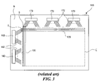
- FIG. 3 is a schematic plan view showing such a COG type LCD device according to the related art.
- an LCD device 100 includes a display area “E” and a non-display area “N.”
- the gate and data lines 120 , 130 crossing each other are disposed in the display area “E.”
- a gate driving unit 160 and a data driving unit 170 are disposed in the non-display area “N.”
- a gate link line 162 connected to the gate line 120 and a data link line 172 connected to the data line 130 are also disposed in the non-display area “N.”
- the gate driving unit 160 is connected to the gate link line 162 through the gate pad portion “G” (shown in FIG.
- a scanning signal output from the gate driving unit 160 is transmitted to the gate line 120 through the gate pad portion “G” and the gate link line 162 and a video signal output from the data driving unit 170 is transmitted to the data line 130 through the data pad portion “D” and the data link line 172 .
- the scanning signal and the video signal are output from a gate output terminal (not shown) and a data output terminal (not shown), respectively.
- the gate output terminal and the data output terminal contact the gate pad portion “G” and the data pad portion “D,” respectively.
- the gate driving unit 160 and the data driving unit 170 are connected to an external printed circuit board (PCB) through a flexible printed circuit (FPC).
- FIG. 4 is a schematic cross-sectional view showing a gate pad portion and a gate output terminal of an LCD device according to the related art.
- a gate pad bump 180 is used as a gate output terminal of a gate driving unit.
- the gate pad bump 180 is electrically connected to the gate pad terminal 144 of a gate pad portion through a plurality of conductive balls 192 in an anisotropic conductive film (ACF) (not shown).
- ACF anisotropic conductive film
- a scanning signal from the gate pad bump 180 is transmitted to the gate pad terminal 144 through the anisotropic conductive balls 192 .
- the scanning signal is transmitted to the gate line 120 (shown FIG. 3 ) through the gate link line 162 (of FIG.
- the gate pad bump 180 is formed of a conductive material such as copper (Cu) or the like.
- the gate pad bump 180 is narrower than the gate pad contact hole 141 in the gate insulating layer 112 and the passivation layer 138 , thereby exposing a portion of the gate pad terminal 144 in the gate pad contact hole 141 .
- FIG. 5 is a schematic plan view showing a gate pad portion and a gate output terminal of an LCD device according to the related art.
- a width of the gate pad bump 180 is less than that of the gate pad contact hole 141 , a portion “C” of the gate pad terminal 144 in the gate pad contact hole 141 is not covered with the gate pad bump 180 and exposed.
- FIGS. 6A and 6B are schematic views illustrating transformation of a plurality of conductive balls according to the related art.
- the conductive ball 192 in an anisotropic conductive film includes first, second and third portions “R1,” “R2” and “R3.”
- the first portion “R1” is formed of a plastic resin
- the second portion “R2” is formed of a metallic material such as nickel (Ni)
- the third portion “R3” is formed of a metallic material such as gold (Au).
- the first portion “R1” has a spherical shape
- the second and third portions “R2” and “R3” have a shell shape.
- the conductive ball 192 has a spherical shape as a whole.
- FIG. 6B when a high pressure and a high temperature are applied, the first portion “R1” of a plastic resin is crushed and the shape is changed. Thus, the entire shape of the conductive ball 292 is also changed according to the transformation of the first portion “R1.”
- the gate pad bump 180 (shown in FIG. 4 ) is electrically connected to the gate pad terminal 144 (shown in FIG. 4 ) by the transformed conductive ball 192 .
- FIG. 7 is a schematic cross-sectional view showing a pressing process for an LCD device according to the related art.
- an anisotropic conductive film (ACF) 190 is interposed between the gate pad bump 180 and a liquid crystal panel 115 .
- the liquid crystal panel 115 includes the gate pad terminal 144 (shown in FIG. 4 ).
- the ACF 190 includes a plurality of conductive balls 192 (shown in FIG. 4 ) surrounded by a thermosetting resin (not shown).
- a heating tool 185 is disposed over the gate pad bump 180 .
- the conductive balls 192 in the ACF 190 may be crushed, thereby contacting the gatepad bump 180 and the gate pad terminal 144 .
- the thermosetting resin is cured with heat and pressure to keep the crushed shapes of the conductive balls 192 .
- the gate pad bump 180 is electrically connected to the gate pad terminal 144 of the liquid crystal panel 115 .
- the heat and the pressure for the transformation of the conductive ball 192 may cause a crack in the gate pad terminal 144 of a transparent conductive material.
- a first portion “A” of the gate pad terminal 144 may be removed by the pressure of the conductive ball 192 to form a crack.
- the gate pad bump 180 does not completely cover the gate pad contact hole 141 , a portion of the gate pad terminal 144 is exposed. Accordingly, external moisture and impurities may be infiltrated into the gate pad 140 through the crack in the gate pad terminal 144 , thereby causing electronic corrosion of the gate pad 140 .
- the gate pad terminal 144 may have a crack at a second portion “B.”
- the second portion “B” corresponds to a step of the gate insulating layer 112 and the passivation layer 138 at the boundary of the gate pad contact hole 141 .
- the external moisture and impurities may be infiltrated into the gate pad 140 through the crack in the gate pad terminal 144 , thereby causing the electronic corrosion of the gate pad 140 .
- the electronic corrosion occurring in the gate pad portion “G” may occur in the data pad portion “D.”
- the present invention is directed to an LCD device and a method of fabricating the LCD device that substantially obviates one or more of the problems caused by limitations and disadvantages of the related art.
- An object of the present invention is to provide an LCD device and a method of fabricating the LCD that electronic corrosion of gate and data pads can be prevented.
- an LCD device includes a gate line and a data line crossing each other, a gate driving unit and a data driving unit outputting signals to the gate line and the data line, a gate pad portion electrically connected to the gate line and having a first contact hole, a data pad portion electrically connected to the data line and having a second contact hole, a first output terminal of the gate driving unit completely covering the first contact hole, a second output terminal of the data driving unit completely covering the second contact hole, a first conductive film electrically connecting the first output terminal and the gate pad portion, and a second conductive film electrically connecting the second output terminal and the data pad portion.
- an LCD device in another aspect, includes first and second substrates having a display area and a non-display area, a gate pad portion and a data pad portion respectively having a gate pad contact hole and a data pad contact hole at the non-display area of the first substrate, a first conductive film and a second conductive film on the gate pad portion and the data pad portion, respectively, and a gate driving unit and a data driving unit on the first conductive film and the second conductive film, respectively, the gate driving unit having a gate pad bump and the data driving unit having a data pad bump, the gate pad bump entirely covering the gate pad contact hole and the data pad bump completely covering the data pad contact hole.
- a method of fabricating an LCD device includes forming a gate pad portion and a data pad portion on a first substrate, the first substrate having a display area and a non-display area, the gate pad portion and the data pad portion in the non-display area, the gate pad portion and the data pad portion having a gate pad contact hole and a data pad contact hole, respectively, forming a first conductive film and a second conductive film on the gate pad portion and the data pad portion, respectively, disposing a gate driving unit having a gate pad bump and a data driving unit having a data pad bump on the first conductive film and the second conductive film, respectively, such that the gate pad bump completely covers the gate pad contact hole and the data pad bump completely covers the data pad contact hole, and applying heat and pressure to the gate driving unit and the data driving unit such that the gate pad bump is electrically connected to the gate pad portion through the first conductive film and the data pad bump is electrically connected to the data pad bump through the second conductive film.
- an LCD device in another aspect, includes a substrate having a display area and non-display area, an electrode pad having a contact hole at the non-display area of the substrate, a driving unit having an electrode pad bump completely covering the contact hole, a conductive film between the electrode pad and the electrode pad bump.
- FIG. 1 is a schematic plan view showing an array substrate for an LCD device according to the related art
- FIG. 2A is a schematic cross-sectional view taken along line “IIa-IIa” of FIG. 1 ;
- FIG. 2B is a schematic cross-sectional view taken along line “IIb-IIb” of FIG. 1 ;
- FIG. 3 is a schematic plan view showing a COG (chip on glass) type LCD device according to the related art
- FIG. 4 is a schematic cross-sectional view showing a gate pad portion and a gate output terminal of an LCD device according to the related art
- FIG. 5 is a schematic plan view showing a gate pad portion and a gate output terminal of an LCD device according to the related art
- FIGS. 6A and 6B are schematic views illustrating transformation of a conductive ball according to the related art
- FIG. 7 is a schematic cross-sectional view showing a pressing process in fabricating an LCD device according to the related art
- FIG. 8 is a schematic cross-sectional view showing a gate pad portion of a COG type LCD device according to an embodiment of the present invention.
- FIG. 9 is a view showing an anisotropic conductive film for the LCD device of FIG. 8 ;
- FIG. 10 is a schematic plan view showing a gate pad portion and a gate output terminal of the LCD device of FIG. 8 ;
- FIG. 11 is a schematic cross-sectional view showing a data pad portion of a COG type LCD device according to another embodiment of the present invention.
- FIG. 12 is a schematic plan view showing a data pad portion and a data output terminal of the LCD device of FIG. 11 .
- FIG. 8 is a schematic cross-sectional view showing a gate pad portion of a chip on glass (COG) type LCD device according to an embodiment of the present invention.
- a gate pad 240 is formed on a substrate 210 .
- a gate insulating layer 212 and a passivation layer 238 are sequentially formed on the gate pad 240 .
- the gate insulating layer 212 and the passivation layer 238 may have a gate pad contact hole 241 exposing a portion of the gate pad 240 .
- a gate pad terminal 244 is formed on the passivation layer 238 and connected to the gate pad 240 through the gate pad contact hole 241 .
- a gate pad bump 280 is formed over the gate pad terminal 244 and a plurality of conductive balls 292 are formed between the gate pad bump 280 and the gate pad terminal 244 .
- the gate pad bump 280 may be used as an output terminal of a gate driving unit (not shown).
- a gate driving unit not shown.
- the gate pad bump 280 completely covers the gate pad contact hole 241 , a portion of the gate pad terminal 244 corresponding to the gate pad contact hole 241 is not exposed.
- the gate pad 240 may be simultaneously formed with a gate line (not shown) in a display area of a liquid crystal panel through the same process.
- the gate pad 240 may be formed of a conductive metallic material such as aluminum (Al), tungsten (W), molybdenum (Mo), chromium (Cr) or the like. After the metallic material is disposed on the substrate 210 , the gate pad 240 may be formed through a photolithographic process and an etch process. If the gate pad 240 is exposed to external moisture and impurities, the gate pad 240 may be electronically corroded. Moreover, static electricity may cause deterioration of the gate line in a subsequent process. Accordingly, the gate pad 240 is protected by forming the gate insulating layer 212 and the passivation layer 238 thereon.
- the gate insulating layer 212 may be formed of one of an inorganic insulating material and an organic insulating material.
- the inorganic insulating material includes silicon oxide (SiO 2 ) and silicon nitride (SiNx) and the organic insulating material includes benzocyclobutene (BCB) and acrylic resin.
- the gate pad contact hole 241 may be formed in the gate insulating layer 212 through a photolithographic process and an etch process.
- the passivation layer 238 may also be formed of one of an inorganic insulating material and an organic insulating material.
- the inorganic insulating material includes silicon oxide (SiO 2 ) and silicon nitride (SiNx) and the organic insulating material includes benzocyclobutene (BCB) and acrylic resin.
- the passivation layer 238 may be formed on the entire surface of the substrate 210 having source and drain electrodes (not shown) in the display area of the liquid crystal panel.
- the gate pad contact hole 241 may be formed in the passivation layer 238 through a photolithographic process and an etch process. In another embodiment, the gate pad contact hole 241 may be formed in the gate insulating layer 212 and the passivation layer 238 after the passivation layer 238 is formed.
- the gate pad terminal 244 is formed of a transparent conductive material such as indium-tin-oxide (ITO), indium-zinc-oxide (IZO) or the like. Since the transparent conductive material is corrosion-resistive and the gate pad terminal 244 shields the gate pad 240 from the exterior, the gate pad terminal 244 may protect the gate pad 140 from the electronic corrosion.
- a scanning signal output from a gate driving unit (not shown) is transmitted to the gate line (not shown) through a gate pad portion including the gate pad 240 and the gate pad terminal 244 .
- the scanning signal of the gate line is transmitted to a TFT to turn on/off the TFT.
- FIG. 9 is a view showing an anisotropic conductive film for an LCD device according to an embodiment of the present invention.
- an anisotropic conductive film (ACF) 290 includes a plurality of conductive balls 292 and a thermosetting resin 293 surrounding the plurality of conductive balls 292 .
- the thermosetting resin 293 is cured, thereby contacting the gate pad bump 280 (shown in FIG. 8 ) and the gate pad terminal 244 (shown in FIG. 8 ).
- the gate pad bump 280 is electrically connected to the gate pad terminal 244 .
- Each of the conductive balls 292 may include a first portion of a plastic resin, a second portion of a metallic material such as nickel (Ni) surrounding the first portion and a third portion of a metallic material such as gold (Au) surrounding the second portion.
- the first portion of a plastic resin provides elasticity to the plurality of conductive balls 292 . When heat and pressure are applied, a plurality of conductive balls 292 are crushed according to the transformation of the first portion of a plastic resin.
- the gate pad bump 280 is electrically connected to the gate pad 240 through the conductive balls 292 .
- the gate pad bump 280 may be formed of a metallic material such as copper (Cu) and transmit a scanning signal to the gate pad terminal 244 .
- the gate pad bump 280 completely covers the gate pad contact hole 241 . In other words, a width of the gate pad bump 280 is greater than that of the gate pad contact hole 241 . Accordingly, any portion of the gate pad terminal 244 corresponding to the gate pad contact hole 241 is not exposed and the electronic corrosion is prevented.
- FIG. 10 is a schematic plan view showing a gate pad portion and a gate output terminal of an LCD device according to an embodiment of the present invention.
- a width of the gate pad bump 280 used as a gate output terminal of a gate driving unit is greater than that of the gate pad contact hole 241 . Accordingly, the gate pad terminal 244 corresponding to the gate pad contact hole 241 is completely covered with the gate pad bump 280 .
- a crack may be created in the gate pad terminal 244 by the pressure of the conductive balls 292 .
- a crack may be created in the gate pad terminal 244 at a step of the gate insulating layer 212 and the passivation layer 238 , i.e., a boundary of the gate pad contact hole 241 .
- the gate pad bump 280 completely covers the gate pad contact hole 241 and the conductive balls 292 in the ACF 290 contacts the gate pad bump 280 and the gate pad terminal 244 .
- the conductive balls 292 and the thermosetting resin 293 over the passivation layer 238 shield the gate pad terminal 244 corresponding to the gate pad contact hole 241 from the exterior with the gate pad bump 280 .
- cracks of the gate pad terminal 244 may be created at a portion corresponding to the conductive balls 292 and a boundary portion (a step portion) of the gate pad contact hole 241 .
- FIG. 11 is a schematic cross-sectional view showing a data pad portion of a chip on glass type LCD device according to an embodiment of the present invention
- FIG. 12 is a schematic plan view showing a data pad portion and a data output terminal of the LCD device of FIG. 11 .
- a data pad bump 281 used as a data output terminal of a data driving unit completely covers a data pad terminal 246 corresponding to a data pad contact hole 243 .
- the data pad bump 281 completely covers the data pad contact hole 243 .
- the data pad terminal 246 corresponding to the data pad contact hole 243 is shielded from the exterior by the data pad bump 281 , the conductive balls 292 and a thermosetting resin over a passivation layer 238 .
- the gate insulating layer 212 is formed on the substrate 210 and a data pad 242 is formed on the gate insulating layer 212 .
- the passivation layer 238 is formed on the data pad 242 .
- the passivation layer 238 has a data pad contact hole 243 exposing a portion of the data pad 242 .
- a data pad terminal 246 is formed on the passivation layer 238 and connected to the data pad 242 through the data pad contact hole 243 .
- the data pad 242 may be simultaneously formed with a data line (not shown) in a display area of a liquid crystal panel through the same process.
- the data pad terminal 246 may be formed of a transparent conductive material such as indium-tin-oxide (ITO), indium-zinc-oxide (IZO) or the like.
- the data pad bump 281 is electrically connected to the data pad terminal 246 through the conductive balls 292 in the ACF 290 .
- the conductive balls 292 and the thermosetting resin over the passivation layer 238 shield the data pad terminal 246 corresponding to the data pad contact hole 243 from the exterior with the data pad bump 281 .
- Cracks of the data pad terminal 246 may be created at portions corresponding to the conductive balls 292 and a boundary portion (a step portion) of the data pad contact hole 243 . All portions where cracks may be created are completely shielded from exterior by the data pad bump 281 , the plurality of conductive balls 292 and the thermosetting resin over the passivation layer 238 . As a result, even when cracks are created, external moisture and impurities will not infiltrate into the data pad 242 through the cracks.
- the gate pad bump completely covers the gate pad contact hole and the data pad bump entirely covers the data pad contact hole, the gate pad and the data pad are shielded from external moisture and impurities. Therefore, the electronic corrosion of the gate pad and the data pad can be prevented.
Abstract
Description
Claims (24)
Applications Claiming Priority (2)
| Application Number | Priority Date | Filing Date | Title |
|---|---|---|---|
| KR2003-0058179 | 2003-08-22 | ||
| KR1020030058179A KR101209489B1 (en) | 2003-08-22 | 2003-08-22 | Liquid crystal display device |
Publications (2)
| Publication Number | Publication Date |
|---|---|
| US20050041189A1 US20050041189A1 (en) | 2005-02-24 |
| US7443479B2 true US7443479B2 (en) | 2008-10-28 |
Family
ID=34192186
Family Applications (1)
| Application Number | Title | Priority Date | Filing Date |
|---|---|---|---|
| US10/879,344 Active US7443479B2 (en) | 2003-08-22 | 2004-06-30 | Liquid crystal display device preventing electronic corrosion and method of fabricating the same |
Country Status (2)
| Country | Link |
|---|---|
| US (1) | US7443479B2 (en) |
| KR (1) | KR101209489B1 (en) |
Cited By (2)
| Publication number | Priority date | Publication date | Assignee | Title |
|---|---|---|---|---|
| US20060181218A1 (en) * | 2005-02-16 | 2006-08-17 | Samsung Electronics Co., Ltd. | Display apparatus and method of manufacturing the same |
| US20070218614A1 (en) * | 2003-04-21 | 2007-09-20 | Seiko Epson Corporation | Semiconductor Device and Method of Manufacturing The Same, Electronic Device and Method of Manufacturing The Same, and Electronic Instrument |
Families Citing this family (11)
| Publication number | Priority date | Publication date | Assignee | Title |
|---|---|---|---|---|
| KR100417916B1 (en) * | 2001-12-29 | 2004-02-14 | 엘지.필립스 엘시디 주식회사 | Array Panel for Liquid Crystal Display Device |
| KR101209489B1 (en) * | 2003-08-22 | 2012-12-07 | 엘지디스플레이 주식회사 | Liquid crystal display device |
| JP2007041389A (en) * | 2005-08-04 | 2007-02-15 | Nec Lcd Technologies Ltd | Display device and its manufacturing method |
| KR100742376B1 (en) * | 2005-09-30 | 2007-07-24 | 삼성에스디아이 주식회사 | Pad area and Method for fabricating the same |
| KR101309319B1 (en) * | 2006-11-22 | 2013-09-13 | 삼성디스플레이 주식회사 | Driving circuit, method of manufacturing thereof and liquid crystal display apparatus having the same |
| KR101330697B1 (en) * | 2006-12-21 | 2013-11-18 | 삼성디스플레이 주식회사 | Display device |
| KR20090089586A (en) * | 2008-02-19 | 2009-08-24 | 삼성모바일디스플레이주식회사 | Organic light emitting display device |
| CN103680317B (en) * | 2013-12-20 | 2015-09-23 | 合肥京东方光电科技有限公司 | A kind of array base palte and manufacture method thereof and display device |
| KR102210523B1 (en) * | 2014-07-17 | 2021-02-02 | 삼성디스플레이 주식회사 | Display Device And Manufacturing Method Thereof |
| KR102422960B1 (en) | 2014-12-29 | 2022-07-21 | 삼성디스플레이 주식회사 | Organic light emitting diode display device and method of manufacturing the same |
| CN106292019B (en) * | 2015-05-20 | 2019-11-29 | 深圳市智化电科技有限公司 | A method of prevent PI in LCD production process from weighing wounded |
Citations (3)
| Publication number | Priority date | Publication date | Assignee | Title |
|---|---|---|---|---|
| US20020145694A1 (en) * | 2001-01-29 | 2002-10-10 | Samsung Electronics Co., Ltd. | Liquid crystal display device and method for manufacturing the same |
| US20050041189A1 (en) * | 2003-08-22 | 2005-02-24 | Lg.Philips Lcd Co., Ltd. | Liquid crystal display device preventing electronic corosion and method of fabricating the same |
| US6934000B1 (en) * | 2000-09-20 | 2005-08-23 | Hitachi, Ltd. | Liquid crystal display |
-
2003
- 2003-08-22 KR KR1020030058179A patent/KR101209489B1/en active IP Right Grant
-
2004
- 2004-06-30 US US10/879,344 patent/US7443479B2/en active Active
Patent Citations (3)
| Publication number | Priority date | Publication date | Assignee | Title |
|---|---|---|---|---|
| US6934000B1 (en) * | 2000-09-20 | 2005-08-23 | Hitachi, Ltd. | Liquid crystal display |
| US20020145694A1 (en) * | 2001-01-29 | 2002-10-10 | Samsung Electronics Co., Ltd. | Liquid crystal display device and method for manufacturing the same |
| US20050041189A1 (en) * | 2003-08-22 | 2005-02-24 | Lg.Philips Lcd Co., Ltd. | Liquid crystal display device preventing electronic corosion and method of fabricating the same |
Cited By (4)
| Publication number | Priority date | Publication date | Assignee | Title |
|---|---|---|---|---|
| US20070218614A1 (en) * | 2003-04-21 | 2007-09-20 | Seiko Epson Corporation | Semiconductor Device and Method of Manufacturing The Same, Electronic Device and Method of Manufacturing The Same, and Electronic Instrument |
| US7662673B2 (en) * | 2003-04-21 | 2010-02-16 | Seiko Epson Corporation | Semiconductor device and method of manufacturing the same, electronic device and method of manufacturing the same, and electronic instrument |
| US20060181218A1 (en) * | 2005-02-16 | 2006-08-17 | Samsung Electronics Co., Ltd. | Display apparatus and method of manufacturing the same |
| US7636145B2 (en) * | 2005-02-16 | 2009-12-22 | Samsung Electronics Co., Ltd. | Display apparatus and method of manufacturing the same |
Also Published As
| Publication number | Publication date |
|---|---|
| KR20050020330A (en) | 2005-03-04 |
| KR101209489B1 (en) | 2012-12-07 |
| US20050041189A1 (en) | 2005-02-24 |
Similar Documents
| Publication | Publication Date | Title |
|---|---|---|
| US6731369B2 (en) | Liquid crystal display device having improved adhesion of a seal pattern | |
| US7633761B2 (en) | Flexible circuit film and display panel assembly having the same | |
| US6737289B2 (en) | Liquid crystal display panel and method for fabricating the same | |
| US6741309B2 (en) | Liquid crystal display | |
| US7956945B2 (en) | Array substrate for liquid crystal display device | |
| JP4178366B2 (en) | Liquid crystal display device and manufacturing method thereof | |
| US7576825B2 (en) | Chip on glass type liquid crystal display device and method for fabricating the same | |
| US20060017873A1 (en) | Liquid crystal display and method for manufacturing the same | |
| KR100470208B1 (en) | Liquid crystal display apparatus of horizontal electronic field applying type and fabricating method thereof | |
| US20060125996A1 (en) | Chip-on-glass array substrate of liquid crystal display device and method of fabricating the same | |
| US8027009B2 (en) | Liquid crystal display device and method of manufacturing the same | |
| US7443479B2 (en) | Liquid crystal display device preventing electronic corrosion and method of fabricating the same | |
| US7943931B2 (en) | Array substrate having a supporter for a data pad, and display apparatus having the array substrate | |
| US8111367B2 (en) | Display device | |
| US8796691B2 (en) | System for displaying images and fabricating method thereof | |
| KR100885378B1 (en) | Liquid crystal display | |
| KR100839149B1 (en) | Liquid crystal display device and method for manufacturing thereof | |
| KR100769435B1 (en) | Liquid crystal display | |
| KR100774578B1 (en) | Liquid crystal display device | |
| JP2008185801A (en) | Method of manufacturing electrooptical device, electrooptical device and electronic device | |
| KR100763407B1 (en) | array panel for liquid crystal display devices | |
| KR100998021B1 (en) | array substrate for in-plane switching mode liquid crystal display device | |
| KR100976980B1 (en) | Flat panel display device | |
| KR20230100044A (en) | Liquid Crystal Display Device | |
| KR101015852B1 (en) | Pad of TFT-LCD |
Legal Events
| Date | Code | Title | Description |
|---|---|---|---|
| AS | Assignment |
Owner name: LG.PHILIPS LCD CO., LTD., KOREA, REPUBLIC OF Free format text: ASSIGNMENT OF ASSIGNORS INTEREST;ASSIGNORS:HONG, JIN-CHEOL;PARK, SUNG-IL;KIM, PYUNG-HUN;AND OTHERS;REEL/FRAME:015545/0581;SIGNING DATES FROM 20040622 TO 20040629 |
|
| AS | Assignment |
Owner name: LG DISPLAY CO., LTD., KOREA, REPUBLIC OF Free format text: CHANGE OF NAME;ASSIGNOR:LG.PHILIPS LCD CO., LTD.;REEL/FRAME:021147/0009 Effective date: 20080319 Owner name: LG DISPLAY CO., LTD.,KOREA, REPUBLIC OF Free format text: CHANGE OF NAME;ASSIGNOR:LG.PHILIPS LCD CO., LTD.;REEL/FRAME:021147/0009 Effective date: 20080319 |
|
| STCF | Information on status: patent grant |
Free format text: PATENTED CASE |
|
| FEPP | Fee payment procedure |
Free format text: PAYOR NUMBER ASSIGNED (ORIGINAL EVENT CODE: ASPN); ENTITY STATUS OF PATENT OWNER: LARGE ENTITY |
|
| FEPP | Fee payment procedure |
Free format text: PAYER NUMBER DE-ASSIGNED (ORIGINAL EVENT CODE: RMPN); ENTITY STATUS OF PATENT OWNER: LARGE ENTITY Free format text: PAYOR NUMBER ASSIGNED (ORIGINAL EVENT CODE: ASPN); ENTITY STATUS OF PATENT OWNER: LARGE ENTITY |
|
| FPAY | Fee payment |
Year of fee payment: 4 |
|
| FPAY | Fee payment |
Year of fee payment: 8 |
|
| MAFP | Maintenance fee payment |
Free format text: PAYMENT OF MAINTENANCE FEE, 12TH YEAR, LARGE ENTITY (ORIGINAL EVENT CODE: M1553); ENTITY STATUS OF PATENT OWNER: LARGE ENTITY Year of fee payment: 12 |