US7410876B1 - Methodology to reduce SOI floating-body effect - Google Patents
Methodology to reduce SOI floating-body effect Download PDFInfo
- Publication number
- US7410876B1 US7410876B1 US11/784,561 US78456107A US7410876B1 US 7410876 B1 US7410876 B1 US 7410876B1 US 78456107 A US78456107 A US 78456107A US 7410876 B1 US7410876 B1 US 7410876B1
- Authority
- US
- United States
- Prior art keywords
- regions
- substrate
- gate electrode
- region
- source
- Prior art date
- Legal status (The legal status is an assumption and is not a legal conclusion. Google has not performed a legal analysis and makes no representation as to the accuracy of the status listed.)
- Expired - Fee Related
Links
- 238000000034 method Methods 0.000 title claims abstract description 59
- 230000000694 effects Effects 0.000 title description 23
- 239000007943 implant Substances 0.000 claims abstract description 42
- 239000000758 substrate Substances 0.000 claims abstract description 28
- 125000006850 spacer group Chemical group 0.000 claims abstract description 22
- 238000005280 amorphization Methods 0.000 claims abstract description 19
- 239000004065 semiconductor Substances 0.000 claims abstract description 15
- 239000002019 doping agent Substances 0.000 claims description 27
- 238000002513 implantation Methods 0.000 claims description 22
- 230000007547 defect Effects 0.000 claims description 20
- 125000001475 halogen functional group Chemical group 0.000 claims description 16
- 238000000137 annealing Methods 0.000 claims description 6
- 229910052786 argon Inorganic materials 0.000 claims description 6
- 229910052785 arsenic Inorganic materials 0.000 claims description 4
- 229910052738 indium Inorganic materials 0.000 claims description 3
- 229910052724 xenon Inorganic materials 0.000 claims description 3
- 229910052787 antimony Inorganic materials 0.000 claims description 2
- 229910052732 germanium Inorganic materials 0.000 claims description 2
- 229910052698 phosphorus Inorganic materials 0.000 claims description 2
- 229910052710 silicon Inorganic materials 0.000 claims description 2
- 230000008569 process Effects 0.000 description 31
- 238000007667 floating Methods 0.000 description 13
- XKRFYHLGVUSROY-UHFFFAOYSA-N Argon Chemical compound [Ar] XKRFYHLGVUSROY-UHFFFAOYSA-N 0.000 description 8
- 238000005215 recombination Methods 0.000 description 8
- 230000006798 recombination Effects 0.000 description 8
- 238000000151 deposition Methods 0.000 description 4
- 230000001965 increasing effect Effects 0.000 description 4
- 239000000463 material Substances 0.000 description 4
- 239000000203 mixture Substances 0.000 description 4
- 235000012431 wafers Nutrition 0.000 description 4
- 238000009792 diffusion process Methods 0.000 description 3
- 239000012535 impurity Substances 0.000 description 3
- 238000010884 ion-beam technique Methods 0.000 description 3
- 238000005457 optimization Methods 0.000 description 3
- 238000001953 recrystallisation Methods 0.000 description 3
- 230000002411 adverse Effects 0.000 description 2
- 238000004380 ashing Methods 0.000 description 2
- 230000008901 benefit Effects 0.000 description 2
- 210000000746 body region Anatomy 0.000 description 2
- 239000000969 carrier Substances 0.000 description 2
- 230000008878 coupling Effects 0.000 description 2
- 238000010168 coupling process Methods 0.000 description 2
- 238000005859 coupling reaction Methods 0.000 description 2
- 230000007423 decrease Effects 0.000 description 2
- 230000008021 deposition Effects 0.000 description 2
- 238000009826 distribution Methods 0.000 description 2
- 238000005530 etching Methods 0.000 description 2
- 239000012212 insulator Substances 0.000 description 2
- 238000004519 manufacturing process Methods 0.000 description 2
- 230000008018 melting Effects 0.000 description 2
- 238000002844 melting Methods 0.000 description 2
- 229920002120 photoresistant polymer Polymers 0.000 description 2
- 229910015890 BF2 Inorganic materials 0.000 description 1
- ZOXJGFHDIHLPTG-UHFFFAOYSA-N Boron Chemical compound [B] ZOXJGFHDIHLPTG-UHFFFAOYSA-N 0.000 description 1
- LEVVHYCKPQWKOP-UHFFFAOYSA-N [Si].[Ge] Chemical compound [Si].[Ge] LEVVHYCKPQWKOP-UHFFFAOYSA-N 0.000 description 1
- 238000007792 addition Methods 0.000 description 1
- 229910021417 amorphous silicon Inorganic materials 0.000 description 1
- RQNWIZPPADIBDY-UHFFFAOYSA-N arsenic atom Chemical compound [As] RQNWIZPPADIBDY-UHFFFAOYSA-N 0.000 description 1
- -1 arsenic ions Chemical class 0.000 description 1
- 230000004888 barrier function Effects 0.000 description 1
- 230000015572 biosynthetic process Effects 0.000 description 1
- 229910052796 boron Inorganic materials 0.000 description 1
- 239000002178 crystalline material Substances 0.000 description 1
- 238000005516 engineering process Methods 0.000 description 1
- 230000005669 field effect Effects 0.000 description 1
- APFVFJFRJDLVQX-UHFFFAOYSA-N indium atom Chemical compound [In] APFVFJFRJDLVQX-UHFFFAOYSA-N 0.000 description 1
- 229910001449 indium ion Inorganic materials 0.000 description 1
- 230000001939 inductive effect Effects 0.000 description 1
- 238000002347 injection Methods 0.000 description 1
- 239000007924 injection Substances 0.000 description 1
- 238000002955 isolation Methods 0.000 description 1
- 238000005224 laser annealing Methods 0.000 description 1
- 229910044991 metal oxide Inorganic materials 0.000 description 1
- 150000004706 metal oxides Chemical class 0.000 description 1
- 238000012986 modification Methods 0.000 description 1
- 230000004048 modification Effects 0.000 description 1
- 230000007935 neutral effect Effects 0.000 description 1
- 230000009467 reduction Effects 0.000 description 1
- 229910021332 silicide Inorganic materials 0.000 description 1
- FVBUAEGBCNSCDD-UHFFFAOYSA-N silicide(4-) Chemical compound [Si-4] FVBUAEGBCNSCDD-UHFFFAOYSA-N 0.000 description 1
- 238000000348 solid-phase epitaxy Methods 0.000 description 1
- 238000006467 substitution reaction Methods 0.000 description 1
- 239000010409 thin film Substances 0.000 description 1
Images


Classifications
-
- H—ELECTRICITY
- H01—ELECTRIC ELEMENTS
- H01L—SEMICONDUCTOR DEVICES NOT COVERED BY CLASS H10
- H01L21/00—Processes or apparatus adapted for the manufacture or treatment of semiconductor or solid state devices or of parts thereof
- H01L21/02—Manufacture or treatment of semiconductor devices or of parts thereof
- H01L21/04—Manufacture or treatment of semiconductor devices or of parts thereof the devices having at least one potential-jump barrier or surface barrier, e.g. PN junction, depletion layer or carrier concentration layer
- H01L21/18—Manufacture or treatment of semiconductor devices or of parts thereof the devices having at least one potential-jump barrier or surface barrier, e.g. PN junction, depletion layer or carrier concentration layer the devices having semiconductor bodies comprising elements of Group IV of the Periodic System or AIIIBV compounds with or without impurities, e.g. doping materials
- H01L21/26—Bombardment with radiation
- H01L21/263—Bombardment with radiation with high-energy radiation
- H01L21/265—Bombardment with radiation with high-energy radiation producing ion implantation
- H01L21/26506—Bombardment with radiation with high-energy radiation producing ion implantation in group IV semiconductors
-
- H—ELECTRICITY
- H01—ELECTRIC ELEMENTS
- H01L—SEMICONDUCTOR DEVICES NOT COVERED BY CLASS H10
- H01L21/00—Processes or apparatus adapted for the manufacture or treatment of semiconductor or solid state devices or of parts thereof
- H01L21/02—Manufacture or treatment of semiconductor devices or of parts thereof
- H01L21/04—Manufacture or treatment of semiconductor devices or of parts thereof the devices having at least one potential-jump barrier or surface barrier, e.g. PN junction, depletion layer or carrier concentration layer
- H01L21/18—Manufacture or treatment of semiconductor devices or of parts thereof the devices having at least one potential-jump barrier or surface barrier, e.g. PN junction, depletion layer or carrier concentration layer the devices having semiconductor bodies comprising elements of Group IV of the Periodic System or AIIIBV compounds with or without impurities, e.g. doping materials
- H01L21/26—Bombardment with radiation
- H01L21/263—Bombardment with radiation with high-energy radiation
- H01L21/265—Bombardment with radiation with high-energy radiation producing ion implantation
- H01L21/2658—Bombardment with radiation with high-energy radiation producing ion implantation of a molecular ion, e.g. decaborane
-
- H—ELECTRICITY
- H01—ELECTRIC ELEMENTS
- H01L—SEMICONDUCTOR DEVICES NOT COVERED BY CLASS H10
- H01L21/00—Processes or apparatus adapted for the manufacture or treatment of semiconductor or solid state devices or of parts thereof
- H01L21/02—Manufacture or treatment of semiconductor devices or of parts thereof
- H01L21/04—Manufacture or treatment of semiconductor devices or of parts thereof the devices having at least one potential-jump barrier or surface barrier, e.g. PN junction, depletion layer or carrier concentration layer
- H01L21/18—Manufacture or treatment of semiconductor devices or of parts thereof the devices having at least one potential-jump barrier or surface barrier, e.g. PN junction, depletion layer or carrier concentration layer the devices having semiconductor bodies comprising elements of Group IV of the Periodic System or AIIIBV compounds with or without impurities, e.g. doping materials
- H01L21/26—Bombardment with radiation
- H01L21/263—Bombardment with radiation with high-energy radiation
- H01L21/265—Bombardment with radiation with high-energy radiation producing ion implantation
- H01L21/26586—Bombardment with radiation with high-energy radiation producing ion implantation characterised by the angle between the ion beam and the crystal planes or the main crystal surface
-
- H—ELECTRICITY
- H01—ELECTRIC ELEMENTS
- H01L—SEMICONDUCTOR DEVICES NOT COVERED BY CLASS H10
- H01L29/00—Semiconductor devices adapted for rectifying, amplifying, oscillating or switching, or capacitors or resistors with at least one potential-jump barrier or surface barrier, e.g. PN junction depletion layer or carrier concentration layer; Details of semiconductor bodies or of electrodes thereof ; Multistep manufacturing processes therefor
- H01L29/02—Semiconductor bodies ; Multistep manufacturing processes therefor
- H01L29/06—Semiconductor bodies ; Multistep manufacturing processes therefor characterised by their shape; characterised by the shapes, relative sizes, or dispositions of the semiconductor regions ; characterised by the concentration or distribution of impurities within semiconductor regions
- H01L29/10—Semiconductor bodies ; Multistep manufacturing processes therefor characterised by their shape; characterised by the shapes, relative sizes, or dispositions of the semiconductor regions ; characterised by the concentration or distribution of impurities within semiconductor regions with semiconductor regions connected to an electrode not carrying current to be rectified, amplified or switched and such electrode being part of a semiconductor device which comprises three or more electrodes
- H01L29/107—Substrate region of field-effect devices
- H01L29/1075—Substrate region of field-effect devices of field-effect transistors
- H01L29/1079—Substrate region of field-effect devices of field-effect transistors with insulated gate
- H01L29/1083—Substrate region of field-effect devices of field-effect transistors with insulated gate with an inactive supplementary region, e.g. for preventing punch-through, improving capacity effect or leakage current
-
- H—ELECTRICITY
- H01—ELECTRIC ELEMENTS
- H01L—SEMICONDUCTOR DEVICES NOT COVERED BY CLASS H10
- H01L29/00—Semiconductor devices adapted for rectifying, amplifying, oscillating or switching, or capacitors or resistors with at least one potential-jump barrier or surface barrier, e.g. PN junction depletion layer or carrier concentration layer; Details of semiconductor bodies or of electrodes thereof ; Multistep manufacturing processes therefor
- H01L29/66—Types of semiconductor device ; Multistep manufacturing processes therefor
- H01L29/66007—Multistep manufacturing processes
- H01L29/66075—Multistep manufacturing processes of devices having semiconductor bodies comprising group 14 or group 13/15 materials
- H01L29/66227—Multistep manufacturing processes of devices having semiconductor bodies comprising group 14 or group 13/15 materials the devices being controllable only by the electric current supplied or the electric potential applied, to an electrode which does not carry the current to be rectified, amplified or switched, e.g. three-terminal devices
- H01L29/66409—Unipolar field-effect transistors
- H01L29/66477—Unipolar field-effect transistors with an insulated gate, i.e. MISFET
- H01L29/66568—Lateral single gate silicon transistors
- H01L29/66659—Lateral single gate silicon transistors with asymmetry in the channel direction, e.g. lateral high-voltage MISFETs with drain offset region, extended drain MISFETs
-
- H—ELECTRICITY
- H01—ELECTRIC ELEMENTS
- H01L—SEMICONDUCTOR DEVICES NOT COVERED BY CLASS H10
- H01L29/00—Semiconductor devices adapted for rectifying, amplifying, oscillating or switching, or capacitors or resistors with at least one potential-jump barrier or surface barrier, e.g. PN junction depletion layer or carrier concentration layer; Details of semiconductor bodies or of electrodes thereof ; Multistep manufacturing processes therefor
- H01L29/66—Types of semiconductor device ; Multistep manufacturing processes therefor
- H01L29/66007—Multistep manufacturing processes
- H01L29/66075—Multistep manufacturing processes of devices having semiconductor bodies comprising group 14 or group 13/15 materials
- H01L29/66227—Multistep manufacturing processes of devices having semiconductor bodies comprising group 14 or group 13/15 materials the devices being controllable only by the electric current supplied or the electric potential applied, to an electrode which does not carry the current to be rectified, amplified or switched, e.g. three-terminal devices
- H01L29/66409—Unipolar field-effect transistors
- H01L29/66477—Unipolar field-effect transistors with an insulated gate, i.e. MISFET
- H01L29/66742—Thin film unipolar transistors
- H01L29/66772—Monocristalline silicon transistors on insulating substrates, e.g. quartz substrates
-
- H—ELECTRICITY
- H01—ELECTRIC ELEMENTS
- H01L—SEMICONDUCTOR DEVICES NOT COVERED BY CLASS H10
- H01L29/00—Semiconductor devices adapted for rectifying, amplifying, oscillating or switching, or capacitors or resistors with at least one potential-jump barrier or surface barrier, e.g. PN junction depletion layer or carrier concentration layer; Details of semiconductor bodies or of electrodes thereof ; Multistep manufacturing processes therefor
- H01L29/66—Types of semiconductor device ; Multistep manufacturing processes therefor
- H01L29/68—Types of semiconductor device ; Multistep manufacturing processes therefor controllable by only the electric current supplied, or only the electric potential applied, to an electrode which does not carry the current to be rectified, amplified or switched
- H01L29/76—Unipolar devices, e.g. field effect transistors
- H01L29/772—Field effect transistors
- H01L29/78—Field effect transistors with field effect produced by an insulated gate
- H01L29/7833—Field effect transistors with field effect produced by an insulated gate with lightly doped drain or source extension, e.g. LDD MOSFET's; DDD MOSFET's
- H01L29/7835—Field effect transistors with field effect produced by an insulated gate with lightly doped drain or source extension, e.g. LDD MOSFET's; DDD MOSFET's with asymmetrical source and drain regions, e.g. lateral high-voltage MISFETs with drain offset region, extended drain MISFETs
-
- H—ELECTRICITY
- H01—ELECTRIC ELEMENTS
- H01L—SEMICONDUCTOR DEVICES NOT COVERED BY CLASS H10
- H01L29/00—Semiconductor devices adapted for rectifying, amplifying, oscillating or switching, or capacitors or resistors with at least one potential-jump barrier or surface barrier, e.g. PN junction depletion layer or carrier concentration layer; Details of semiconductor bodies or of electrodes thereof ; Multistep manufacturing processes therefor
- H01L29/66—Types of semiconductor device ; Multistep manufacturing processes therefor
- H01L29/68—Types of semiconductor device ; Multistep manufacturing processes therefor controllable by only the electric current supplied, or only the electric potential applied, to an electrode which does not carry the current to be rectified, amplified or switched
- H01L29/76—Unipolar devices, e.g. field effect transistors
- H01L29/772—Field effect transistors
- H01L29/78—Field effect transistors with field effect produced by an insulated gate
- H01L29/786—Thin film transistors, i.e. transistors with a channel being at least partly a thin film
- H01L29/78606—Thin film transistors, i.e. transistors with a channel being at least partly a thin film with supplementary region or layer in the thin film or in the insulated bulk substrate supporting it for controlling or increasing the safety of the device
- H01L29/78612—Thin film transistors, i.e. transistors with a channel being at least partly a thin film with supplementary region or layer in the thin film or in the insulated bulk substrate supporting it for controlling or increasing the safety of the device for preventing the kink- or the snapback effect, e.g. discharging the minority carriers of the channel region for preventing bipolar effect
-
- H—ELECTRICITY
- H01—ELECTRIC ELEMENTS
- H01L—SEMICONDUCTOR DEVICES NOT COVERED BY CLASS H10
- H01L29/00—Semiconductor devices adapted for rectifying, amplifying, oscillating or switching, or capacitors or resistors with at least one potential-jump barrier or surface barrier, e.g. PN junction depletion layer or carrier concentration layer; Details of semiconductor bodies or of electrodes thereof ; Multistep manufacturing processes therefor
- H01L29/66—Types of semiconductor device ; Multistep manufacturing processes therefor
- H01L29/68—Types of semiconductor device ; Multistep manufacturing processes therefor controllable by only the electric current supplied, or only the electric potential applied, to an electrode which does not carry the current to be rectified, amplified or switched
- H01L29/76—Unipolar devices, e.g. field effect transistors
- H01L29/772—Field effect transistors
- H01L29/78—Field effect transistors with field effect produced by an insulated gate
- H01L29/786—Thin film transistors, i.e. transistors with a channel being at least partly a thin film
- H01L29/78606—Thin film transistors, i.e. transistors with a channel being at least partly a thin film with supplementary region or layer in the thin film or in the insulated bulk substrate supporting it for controlling or increasing the safety of the device
- H01L29/78618—Thin film transistors, i.e. transistors with a channel being at least partly a thin film with supplementary region or layer in the thin film or in the insulated bulk substrate supporting it for controlling or increasing the safety of the device characterised by the drain or the source properties, e.g. the doping structure, the composition, the sectional shape or the contact structure
- H01L29/78621—Thin film transistors, i.e. transistors with a channel being at least partly a thin film with supplementary region or layer in the thin film or in the insulated bulk substrate supporting it for controlling or increasing the safety of the device characterised by the drain or the source properties, e.g. the doping structure, the composition, the sectional shape or the contact structure with LDD structure or an extension or an offset region or characterised by the doping profile
- H01L29/78624—Thin film transistors, i.e. transistors with a channel being at least partly a thin film with supplementary region or layer in the thin film or in the insulated bulk substrate supporting it for controlling or increasing the safety of the device characterised by the drain or the source properties, e.g. the doping structure, the composition, the sectional shape or the contact structure with LDD structure or an extension or an offset region or characterised by the doping profile the source and the drain regions being asymmetrical
-
- H—ELECTRICITY
- H01—ELECTRIC ELEMENTS
- H01L—SEMICONDUCTOR DEVICES NOT COVERED BY CLASS H10
- H01L29/00—Semiconductor devices adapted for rectifying, amplifying, oscillating or switching, or capacitors or resistors with at least one potential-jump barrier or surface barrier, e.g. PN junction depletion layer or carrier concentration layer; Details of semiconductor bodies or of electrodes thereof ; Multistep manufacturing processes therefor
- H01L29/66—Types of semiconductor device ; Multistep manufacturing processes therefor
- H01L29/66007—Multistep manufacturing processes
- H01L29/66075—Multistep manufacturing processes of devices having semiconductor bodies comprising group 14 or group 13/15 materials
- H01L29/66227—Multistep manufacturing processes of devices having semiconductor bodies comprising group 14 or group 13/15 materials the devices being controllable only by the electric current supplied or the electric potential applied, to an electrode which does not carry the current to be rectified, amplified or switched, e.g. three-terminal devices
- H01L29/66409—Unipolar field-effect transistors
- H01L29/66477—Unipolar field-effect transistors with an insulated gate, i.e. MISFET
- H01L29/6656—Unipolar field-effect transistors with an insulated gate, i.e. MISFET using multiple spacer layers, e.g. multiple sidewall spacers
Definitions
- the present disclosure relates generally to semiconductor devices built on SOI layers, and more particularly to methods for controlling the floating body effect in SOI MOSFETs.
- MOSFETs Metal Oxide Semiconductor Field Effect Transistors
- MOSFET devices were frequently fabricated as bulk semiconductor devices in which the device features were defined on the surface of a bulk semiconductor wafer.
- MOSFET devices have continued to shrink in size, and as the transistor densities in these devices have increased accordingly, the disadvantages associated with bulk MOSFETs have become increasingly apparent. These disadvantages include an often less than ideal sub-threshold voltage rolloff, short channel effects, drain induced barrier lowering, high junction capacitance, ineffective isolation, and low saturation current.
- SOI wafers feature a thin semiconductor layer which is disposed over a (typically oxide) dielectric layer.
- Transistors fabricated on such wafers offer the potential of superior performance characteristics due to the thin film nature of the semiconductor substrate and the electrically insulating properties of the underlying dielectric layer.
- SOI MOSFETs may manifest superior short channel performance, near-ideal subthreshold voltage swings (which results in low off-state current leakage), and high saturation current.
- SOI devices present their own set of challenges.
- One of these challenges is the floating-body effect, a phenomenon manifested as a decrease in voltage between the source and the drain regions. This effect is especially problematic for partially depleted SOI MOSFETs of the type currently used in some memory devices.
- FIG. 1 is an illustration of a step in a prior art process for making a MOSFET device
- FIG. 2 is an illustration of a step in a prior art process for making a MOSFET device
- FIG. 3 is an illustration of a step in a prior art process for making a MOSFET device
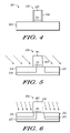
- FIG. 4 is an illustration of a step in a process for making a MOSFET device in accordance with the teachings herein;
- FIG. 5 is an illustration of a step in a process for making a MOSFET device in accordance with the teachings herein;
- FIG. 6 is an illustration of a step in a process for making a MOSFET device in accordance with the teachings herein;
- FIG. 7 is an illustration of a step in a process for making a MOSFET device in accordance with the teachings herein;
- FIG. 8 is an illustration of a step in a process for making a MOSFET device in accordance with the teachings herein;
- FIG. 9 is an illustration of a step in a process for making a MOSFET device in accordance with the teachings herein;
- FIG. 10 is an illustration of a step in a process for making a MOSFET device in accordance with the teachings herein;
- FIG. 11 is an illustration of a step in a process for making a MOSFET device in accordance with the teachings herein;
- FIG. 12 is an illustration of a step in a process for making a MOSFET device in accordance with the teachings herein;
- FIG. 13 is an illustration of a step in a process for making a MOSFET device in accordance with the teachings herein;
- FIG. 14 is a graph of % (V TLIN ⁇ V TSAT )V DD as a function of supply voltage (V);
- FIG. 15 is a graph of drain current (A) as a function of gate voltage (V).
- FIG. 16 is a graph of off-leak current (A/ ⁇ m) as a function of Ar dose.
- a method for making a semiconductor device comprises a gate electrode disposed on a substrate.
- First and second pre-amorphization implant regions are created in the substrate such that the first and second pre-amorphization implant regions are asymmetrically disposed with respect to said gate electrode.
- First and second spacer structures are created adjacent to first and second sides of the gate electrode such that the first and second spacer structures overlap the first and second pre-amorphization implant regions, respectively.
- Source and drain regions are then created in the substrate adjacent, respectively, to the first and second spacer structures.
- the floating-body effect is believed to be caused by impact ionization in the channel region during on-state operation.
- impact ionization typically occurs near the drain side of the channel region.
- carriers accumulate in the body of the SOI transistor, thereby increasing the potential between the channel region and the drain region.
- the increased potential reduces the threshold voltage of the transistor which, in turn, adversely affects the stability and power consumption of the transistor, increases its off-state and on-state current, and adversely affects the stability of the device.
- the body potential immediately after commencement of circuit operation is influenced by the body potential of the device in the off-state of the circuit, this potential changes as the circuit continues to operate, and in some cases reaches a fixed value. Until that fixed value is reached, the drain current of the transistor continues to fluctuate due to the fluctuations in the body potential.
- control of the floating body effect may be obtained through the provision of recombination centers in the source side of a transistor, which quickly drop the body potential of the device.
- These recombination centers may be formed through the selective implantation at a highly tilted angle of an appropriate species, such as, for example, Ar, Ge or Xe, at the source side of the transistor.
- FIGS. 1-3 which is a prior art process for making a semiconductor device.
- an SOI MOSFET 12 comprises a substrate 14 which includes a semiconductor-on-insulator (SOI) semiconductor layer 15 , a dielectric layer 17 , and a semiconductor substrate layer 19 .
- the SOI MOSFET 12 further includes a gate structure 18 , a source region 22 , and a drain region 24 .
- the source 22 and drain 24 regions extend from the top 27 to the bottom 55 of the SOI layer 15 (top surface of layer 17 ), and include source extension 23 and drain extension 25 regions, respectively.
- regions 22 and 24 are heavily doped with N-type dopants
- regions 22 and 24 are heavily doped with P-type dopants.
- the gate structure 18 also includes a pair of spacers 38 , and a gate electrode 36 disposed between a source location associated with region 22 and a drain location associated with region 24 .
- the gate structure 18 is placed over a channel region 41 disposed between extensions 23 and 25 .
- Drain region 24 includes deep drain region 35
- source region 22 includes deep source region 33 .
- Regions 33 and 35 are deeper than extensions 23 and 25 .
- Source region 22 includes an abrupt junction 52 extending in a vertical direction from extension 23 to bottom 55 .
- junction 52 is disposed underneath spacer 38 closer to an edge 56 of the gate electrode 36 than an edge 57 of spacer 38 .
- a junction 62 (below extension 25 ) of drain region 24 is disposed closer to an edge 67 of spacer 38 than an edge 65 of the gate electrode 36 . Accordingly, the source region 22 and drain region 24 are asymmetrical.
- junction 52 is a very abrupt junction disposed in the subsurface of the source-body junction (e.g., the interface between region 22 and region 41 ), thereby providing high carrier injection from source region 22 .
- FIG. 2 illustrates a conventional double implant process which is used to form source 22 and drain 24 regions, including extensions 23 and 25 thereof.
- the dopants for the source region 22 and drain region 24 are medium or light mass dopants, such as boron.
- a high temperature annealing process may be performed.
- the high temperature annealing process may be a rapid thermal anneal (RTA) to activate the dopants in regions 22 and 24 .
- RTA rapid thermal anneal
- the high temperature anneal process used to activate the dopants will also concurrently anneal most of the damage caused by the implant process.
- the structure is then subjected to an angled dopant implant to form the junction 52 (see FIG. 1 ).
- the angled dopant implant may be performed at an angle of 20°-70° from a top surface 27 of layer 15 (see FIG. 1 ).
- the N-type regions delineated by dashed lines 66 and 68 may be formed with an N-type dopant, such as arsenic.
- the implant extends from the top surface 27 to bottom 55 of layer 15 .
- line 66 extends underneath gate structure 18 while line 68 is set apart from gate structure 18 .
- the shadowing effect associated with gate structure 18 protects the area underneath extension 25 from the N-type dopants.
- P-type dopants such as Indium, may be used to form P-type regions delineated by dashed lines 66 and 68 .
- the regions defined by lines 66 and 68 can be amorphous or partially amorphous due to the implantation step.
- Portion 10 is subjected to a laser annealing process.
- the regions defined by dashed lines 66 and 68 become molten and are recrystallized after the laser beam is removed.
- the recrystallization process forms an abrupt junction 52 (an abrupt lateral junction on the source side of transistor 12 ).
- the annealing process can raise the temperature of regions defined by lines 66 and 68 to the melting temperature of the regions (1100° C. for amorphous silicon germanium).
- the melting temperature of the regions in the amorphous state is significantly lower than that of substrate 14 (layer 15 ) which is in a crystalline state.
- the laser fluence may be controlled so that the regions defined by lines 66 and 68 are fully melted and layer 15 is not melted.
- regions defined by lines 66 and 68 are recrystallized as a single crystalline material.
- the annealing process can be a solid phase epitaxy process. After annealing, conventional fabrication processes and techniques can be utilized to form silicide layers, interconnects, contacts, and the like.
- FIGS. 4-8 illustrate a first particular, non-limiting embodiment of a process for making an SOI transistor in accordance with the teachings herein.
- a semiconductor structure 201 is provided which comprises an SOI layer 203 having a gate structure 205 defined thereon.
- the gate structure 205 comprises a gate electrode 207 insulated from the SOI layer 203 by way of a gate oxide 211 .
- the sides of the gate electrode 207 are likewise covered with a layer of oxide 209 which may have a composition which is the same as, or different from, the composition of gate oxide 211 .
- the structure is subjected to pre-amorphization implantation (PAI) with an ion beam to form first 213 and second 213 amorphized implant regions.
- PAI pre-amorphization implantation
- the PAI may be accomplished by implanting a suitable impurity (such as, for example, Si, Ge, Sb, In, As, P, BF 2 , Xe or Ar) of a first conductivity type into the SOI layer 203 at a high tilt angle.
- a suitable impurity such as, for example, Si, Ge, Sb, In, As, P, BF 2 , Xe or Ar
- the conductivity type of the impurity used in this step is neutral or preferably opposite to the conductivity type of the dopant type used in the later formed source 217 and drain 218 regions (see FIG. 8 ).
- the tilt angle used for the pre-amorphization implantation is preferably within the range of about 20° to about 70°, more preferably within the range of about 30° to about 60°, and most preferably within the range of about 40° to about 50°.
- the use of a high angle for this implantation step has a shadowing effect (that is, the portion of the amorphized implant region 213 on the source side of the gate structure 205 extends underneath the gate structure 205 , while the portion of the amorphized implant region 213 on the drain side of the gate structure 205 is spaced apart from the gate structure 205 ).
- the amorphized implant region 213 may have characteristics which vary with depth. For example, the degree of crystallinity may vary as a function of depth throughout the amorphized implant region 213 .
- source 215 and drain 215 extension regions are then created by implantation of a species of a second conductivity type using the gate structure 205 as an implant mask.
- the implantation is performed at a steeper (but nonzero) angle compared to the PAI implant, and hence the source 215 and drain 215 extension regions are formed asymmetrically about the gate electrode 207 .
- the angle for this implantation is preferably within the range of about 5° to about 45°, more preferably within the range of about 5° to about 30°, and most preferably within the range of about 10° to about 20°.
- asymmetric halo regions are then formed by implantation of a species of a second conductivity type using the gate structure 205 as an implant mask.
- the halo regions are formed with a p-type dopant.
- the halo implantation is preferably performed at a similar angle to the PAI.
- spacer structures 219 , 220 are formed adjacent to the gate electrode 207 by depositing a suitable spacer material over the structure, and then subjecting the spacer material to anisotropic etching. A deep implant is then conducted, followed by an anneal, to form source 217 and drain 218 regions. The anneal may induce some diffusion in the dopant used to define the source 217 and drain 218 regions.
- the anneal In addition to inducing diffusion in the dopant used to define the source 217 and drain 218 regions, the anneal also promotes recrystallization in the amorphous regions. As seen in FIG. 8 , this results in the formation of end of range (EOR) defects 221 in these regions. Since the PAI region 213 is asymmetric, the EOR defects 221 are disposed asymmetrically about the gate electrode 205 . Under suitable implant and anneal conditions, these EOR defects 221 form lines of defects. This results in source 217 EOR defects 221 being disposed closer to the center of the gate electrode than the drain 218 EOR defects 221 . Hence, the EOR defects 221 introduce recombination centers preferentially in the source side of the device.
- EOR defects 221 introduce recombination centers preferentially in the source side of the device.
- these recombination centers help to control the floating body wherein the recombination centers due to the source 217 EOR defects have a stronger impact on the floating body potential than the recombination centers due to the drain 218 EOR defects.
- FIGS. 4-8 is advantageous over the process depicted in FIGS. 1-3 in that, by forming the first 213 and second 214 amorphized implant regions prior to forming the spacer structures 219 and 220 , an additional sequence of photoresist deposition, implantation, and ashing is avoided.
- CMOS transistors made in accordance with the teachings herein in which different species are utilized to form the source and drain regions in the NMOS and PMOS regions of the device (for example, where arsenic ions are used to define the source and drain regions in the NMOS region of the device, and indium ions are used to define the source and drain regions in the PMOS region of the device), a second additional sequence of photoresist deposition, implantation, and ashing is avoided.
- FIGS. 9-13 illustrate a second particular, non-limiting embodiment of a process for making an SOI transistor in accordance with the teachings herein.
- a semiconductor structure 301 which comprises an SOI layer 303 having a gate structure 305 defined thereon.
- the gate structure 305 comprises a gate electrode 307 insulated from the SOI layer 303 by way of a gate oxide 311 .
- the sides of the gate electrode 307 are likewise covered with a layer of oxide 309 which may have a composition which is the same as, or different from, the composition of gate oxide 311 .
- the structure is subjected to a first pre-amorphization implantation (PAI) with an ion beam using a first dopant species to form a first set of PAI regions 313 , 314 .
- the PAI may be accomplished by implanting a suitable impurity of a first conductivity type into the SOI layer 303 at a high tilt angle in a manner analogous to the step depicted in FIG. 5 .
- this PAI implant may be done after junction profile optimization by the second PAI, extension and halo implantation described below.
- the structure is then subjected to second PAI with an ion beam using a second dopant species to form a second set of PAI regions 315 , 316 which can be used for junction profile optimization in combination with subsequent extension and halo implants.
- the second set of PAI regions 315 , 316 may be formed by implanting a second dopant species of a first conductivity type into the SOI layer 303 .
- the tilt angle for the implantation step is essentially zero.
- the second set of PAI regions 315 , 316 is formed at a lower energy, and hence the second set of PAI regions 315 , 316 is shallower than the first set of PAI regions 313 , 314 .
- source 317 and drain 318 extensions are then created by implantation of a species of a second conductivity type using the gate structure 305 as an implant mask, in a manner analogous to that depicted in FIG. 6 .
- the implantation is performed at a steeper (but nonzero) angle compared to the PAI implant, and hence the source 317 and drain 318 extensions are formed asymmetrically about the gate electrode 307 .
- asymmetric halo regions are then formed by implantation of a species of a first conductivity type using the gate structure 305 as an implant mask.
- the halo regions are formed with a p-type dopant.
- the halo implantation is preferably performed at a similar angle to the PAI.
- spacer structures 319 , 320 are formed adjacent to the gate electrode 307 by depositing a suitable spacer material over the structure, and then subjecting the spacer material to anisotropic etching. A deep implant is then conducted, followed by an anneal, to form source 321 and drain 322 regions. The anneal may induce some diffusion in the dopant used to define the source 321 and drain 322 regions.
- the anneal results in recrystallization in the amorphous regions, and anneals out most of the defects, while leaving behind end of range (EOR) defects 321 in these regions.
- EOR defects 321 form lines of defects. Since the first set of PAI regions 313 , 314 and the second set of PAI regions 315 , 316 are asymmetrically disposed about the gate electrode 307 , the EOR defects 321 form regions which are disposed asymmetrically about the gate electrode 305 such that the line of source EOR defects 321 is disposed closer to the center of the gate electrode than the line of drain EOR defects 321 .
- the EOR defects 321 introduce recombination centers preferentially in the source side of the device which, as previously noted, is believed to help to control the floating body effect by strongly influencing the body potential.
- FIGS. 9-13 is advantageous in that it utilizes two separate pre-amorphization implants, one for optimization of the halo and source/drain extension regions, and another for floating body reduction. Such an approach may be particularly useful where it is not possible to simultaneously achieve both of these ends with a single pre-amorphization implant, as may be the case where these goals represent competing considerations.
- FIG. 14 illustrates floating body potential as a function of supply voltage for an SOI device.
- the graph shows the results obtained at two different temperatures both with, and without, PAI.
- the PAI in this case was conducted with Argon as the dopant.
- PAI significantly reduced floating body potential at both temperatures.
- FIGS. 15-16 The effect of a highly tilted PAI of the type depicted in FIGS. 5 and 9 is further demonstrated with reference to the graphs depicted in FIGS. 15-16 .
- drain current as a function of voltage was measured at positive and negative potentials for analogous devices formed with (a) a 7° PAI using Argon; (b) a 40° PAI using Argon; and (c) no PAI.
- the graph in FIG. 16 shows off-leakage current as a function of Argon dosage for the 7° and 40° implantations referenced in FIG. 15 . As these graphs show, the floating body effect was observed to decline with increasing tilt angle.
Abstract
Description
Claims (19)
Priority Applications (1)
| Application Number | Priority Date | Filing Date | Title |
|---|---|---|---|
| US11/784,561 US7410876B1 (en) | 2007-04-05 | 2007-04-05 | Methodology to reduce SOI floating-body effect |
Applications Claiming Priority (1)
| Application Number | Priority Date | Filing Date | Title |
|---|---|---|---|
| US11/784,561 US7410876B1 (en) | 2007-04-05 | 2007-04-05 | Methodology to reduce SOI floating-body effect |
Publications (1)
| Publication Number | Publication Date |
|---|---|
| US7410876B1 true US7410876B1 (en) | 2008-08-12 |
Family
ID=39678699
Family Applications (1)
| Application Number | Title | Priority Date | Filing Date |
|---|---|---|---|
| US11/784,561 Expired - Fee Related US7410876B1 (en) | 2007-04-05 | 2007-04-05 | Methodology to reduce SOI floating-body effect |
Country Status (1)
| Country | Link |
|---|---|
| US (1) | US7410876B1 (en) |
Cited By (14)
| Publication number | Priority date | Publication date | Assignee | Title |
|---|---|---|---|---|
| US20080254586A1 (en) * | 2007-04-12 | 2008-10-16 | Min Byoung W | Soi semiconductor device with body contact and method thereof |
| US20090298249A1 (en) * | 2008-05-30 | 2009-12-03 | Jan Hoentschel | Drive current increase in transistors by asymmetric amorphization implantation |
| US20100216288A1 (en) * | 2009-02-23 | 2010-08-26 | Yihang Chiu | Fabrication of Source/Drain Extensions with Ultra-Shallow Junctions |
| US20100264469A1 (en) * | 2009-04-20 | 2010-10-21 | International Business Machines Corporation | Mosfet including epitaxial halo region |
| CN101916726A (en) * | 2010-07-06 | 2010-12-15 | 中国科学院上海微系统与信息技术研究所 | Method for manufacturing signal operation instruction (SOI) metal oxide semiconductor (MOS) apparatus structure for restraining floating body effect |
| CN101950723A (en) * | 2010-07-06 | 2011-01-19 | 中国科学院上海微系统与信息技术研究所 | Method for manufacturing SOI MOS device capable of realizing ohmic contact with source body |
| US20110049625A1 (en) * | 2009-08-31 | 2011-03-03 | Chartered Semiconductor Manufacturing, Ltd. | Asymmetrical transistor device and method of fabrication |
| US20110065244A1 (en) * | 2009-09-15 | 2011-03-17 | International Business Machines Corporation | Asymmetric finfet device with improved parasitic resistance and capacitance |
| US20110193166A1 (en) * | 2010-02-05 | 2011-08-11 | International Business Machines Corporation | Structure and method for reducing floating body effect of soi mosfets |
| WO2012034346A1 (en) * | 2010-09-15 | 2012-03-22 | 中国科学院微电子研究所 | Transistor and fabricaing method thereof |
| US8633078B2 (en) | 2010-10-28 | 2014-01-21 | Samsung Electronics Co., Ltd. | Method for manufacturing semiconductor device |
| US20140346576A1 (en) * | 2011-10-24 | 2014-11-27 | Taiwan Semiconductor Manufacturing Company, Ltd. | Mosfets with multiple dislocation planes |
| US8952429B2 (en) | 2010-09-15 | 2015-02-10 | Institute of Microelectronics, Chinese Academy of Sciences | Transistor and method for forming the same |
| CN109427887A (en) * | 2017-08-29 | 2019-03-05 | 中芯国际集成电路制造(上海)有限公司 | A kind of manufacturing method and semiconductor devices of semiconductor devices |
Citations (13)
| Publication number | Priority date | Publication date | Assignee | Title |
|---|---|---|---|---|
| US5780912A (en) | 1994-08-18 | 1998-07-14 | Sun Microsystems, Inc. | Asymmetric low power MOS devices |
| US6534373B1 (en) | 2001-03-26 | 2003-03-18 | Advanced Micro Devices, Inc. | MOS transistor with reduced floating body effect |
| US6855592B2 (en) * | 2001-12-15 | 2005-02-15 | Hynix Semiconductor Inc. | Method for manufacturing semiconductor device |
| US20050136623A1 (en) | 2003-12-22 | 2005-06-23 | Tan Chung F. | Shallow amorphizing implant for gettering of deep secondary end of range defects |
| US6916716B1 (en) | 2003-10-24 | 2005-07-12 | Advanced Micro Devices, Inc. | Asymmetric halo implants |
| US20050164461A1 (en) | 2004-01-27 | 2005-07-28 | Yu-Kun Chen | Method for forming a junction region of a semiconductor device |
| US20060043430A1 (en) | 2004-08-31 | 2006-03-02 | Thomas Feudel | Transistor having an asymmetric source/drain and halo implantation region and a method of forming the same |
| US20060216899A1 (en) * | 2005-03-22 | 2006-09-28 | Ming-Tsung Chen | Silicide process utilizing pre-amorphization implant and second spacer |
| US7118980B2 (en) | 2004-10-25 | 2006-10-10 | Texas Instruments Incorporated | Solid phase epitaxy recrystallization by laser annealing |
| US20060284249A1 (en) * | 2005-06-21 | 2006-12-21 | Chien-Hao Chen | Impurity co-implantation to improve transistor performance |
| US20070037326A1 (en) * | 2005-08-09 | 2007-02-15 | Taiwan Semiconductor Manufacturing Company, Ltd. | Shallow source/drain regions for CMOS transistors |
| US20070252205A1 (en) * | 2006-04-28 | 2007-11-01 | Jan Hoentschel | Soi transistor having a reduced body potential and a method of forming the same |
| US7354839B2 (en) * | 2005-02-28 | 2008-04-08 | Advanced Micro Devices, Inc. | Gate structure and a transistor having asymmetric spacer elements and methods of forming the same |
-
2007
- 2007-04-05 US US11/784,561 patent/US7410876B1/en not_active Expired - Fee Related
Patent Citations (14)
| Publication number | Priority date | Publication date | Assignee | Title |
|---|---|---|---|---|
| US5780912A (en) | 1994-08-18 | 1998-07-14 | Sun Microsystems, Inc. | Asymmetric low power MOS devices |
| US6534373B1 (en) | 2001-03-26 | 2003-03-18 | Advanced Micro Devices, Inc. | MOS transistor with reduced floating body effect |
| US6855592B2 (en) * | 2001-12-15 | 2005-02-15 | Hynix Semiconductor Inc. | Method for manufacturing semiconductor device |
| US6916716B1 (en) | 2003-10-24 | 2005-07-12 | Advanced Micro Devices, Inc. | Asymmetric halo implants |
| US20050136623A1 (en) | 2003-12-22 | 2005-06-23 | Tan Chung F. | Shallow amorphizing implant for gettering of deep secondary end of range defects |
| US20050164461A1 (en) | 2004-01-27 | 2005-07-28 | Yu-Kun Chen | Method for forming a junction region of a semiconductor device |
| US20060043430A1 (en) | 2004-08-31 | 2006-03-02 | Thomas Feudel | Transistor having an asymmetric source/drain and halo implantation region and a method of forming the same |
| US7118980B2 (en) | 2004-10-25 | 2006-10-10 | Texas Instruments Incorporated | Solid phase epitaxy recrystallization by laser annealing |
| US7354839B2 (en) * | 2005-02-28 | 2008-04-08 | Advanced Micro Devices, Inc. | Gate structure and a transistor having asymmetric spacer elements and methods of forming the same |
| US20060216899A1 (en) * | 2005-03-22 | 2006-09-28 | Ming-Tsung Chen | Silicide process utilizing pre-amorphization implant and second spacer |
| US20060252213A1 (en) | 2005-03-22 | 2006-11-09 | Ming-Tsung Chen | Silicide process utilizing pre-amorphization implant and second spacer |
| US20060284249A1 (en) * | 2005-06-21 | 2006-12-21 | Chien-Hao Chen | Impurity co-implantation to improve transistor performance |
| US20070037326A1 (en) * | 2005-08-09 | 2007-02-15 | Taiwan Semiconductor Manufacturing Company, Ltd. | Shallow source/drain regions for CMOS transistors |
| US20070252205A1 (en) * | 2006-04-28 | 2007-11-01 | Jan Hoentschel | Soi transistor having a reduced body potential and a method of forming the same |
Non-Patent Citations (8)
| Title |
|---|
| Bergaud, C. et al., "Formation of Implanted Piezoresistors Under 100-NM Thick for Nanoelectromechanical Systems"; IEEE, 2002, pp. 360-363. |
| Borland, John O. et al., "Applying Equivalent Scaling to USJ Implantation"; Semiconductor International; Jan. 1, 2005; 8 pages; www.reed-electronics.com/semiconductor. |
| Borland, John.; "Implantation and Annealing Options for 65 nm Node SDE Formation"; Apr. 1, 2003; 2 pages; www.reed-electronics.com/semiconductor. |
| Chang, D. et al., "Efficacy of Ar in Reducing the Kink Effect on Floating-Body NFD/SOI CMOS"; Proceedings 1998 EIII International SOI Conference; Oct. 1998; pp. 155-156. |
| Chen, Vincent M.C. and Woo, Jason C.S., "Tunneling Source-Body Contact for Partially-Depleted SOI MOSFET"; IEEE Trans. on Elect. Dev., V. 44, No. 7, Jul. 1997, pp. 1143-1147. |
| Matloubian, M., "Smart Body Contact for SOI MOSFETs", Semiconductor Process and Design Center, Texas Instruments Inc.; Intl. SOI Conf., 1989, pp. 128-129. |
| Ohno, T. et al., "Supp. of the Parasitic Bipolar Effect in Ultra-Thin-Film nMOSFETs/SIMOX by Ar Ion Implant. into Source/Drain Regions"; 1995, IEEE, pp. IEDM 95-627-630. |
| Wei, H.F. et al., "Improvement of Breakdown Voltage and Off-State Leakage in Ge-Implanted SOI n-MOSFETs"; IEEE, 1993, pp. IEDM 93-739-742. |
Cited By (30)
| Publication number | Priority date | Publication date | Assignee | Title |
|---|---|---|---|---|
| US7927934B2 (en) | 2007-04-12 | 2011-04-19 | Freescale Semiconductor, Inc. | SOI semiconductor device with body contact and method thereof |
| US20080254586A1 (en) * | 2007-04-12 | 2008-10-16 | Min Byoung W | Soi semiconductor device with body contact and method thereof |
| US20090298249A1 (en) * | 2008-05-30 | 2009-12-03 | Jan Hoentschel | Drive current increase in transistors by asymmetric amorphization implantation |
| US7855118B2 (en) * | 2008-05-30 | 2010-12-21 | Advanced Micro Devices, Inc. | Drive current increase in transistors by asymmetric amorphization implantation |
| US8173503B2 (en) * | 2009-02-23 | 2012-05-08 | Taiwan Semiconductor Manufacturing Co., Ltd. | Fabrication of source/drain extensions with ultra-shallow junctions |
| US20100216288A1 (en) * | 2009-02-23 | 2010-08-26 | Yihang Chiu | Fabrication of Source/Drain Extensions with Ultra-Shallow Junctions |
| US20100264469A1 (en) * | 2009-04-20 | 2010-10-21 | International Business Machines Corporation | Mosfet including epitaxial halo region |
| US7829939B1 (en) * | 2009-04-20 | 2010-11-09 | International Business Machines Corporation | MOSFET including epitaxial halo region |
| US20110049625A1 (en) * | 2009-08-31 | 2011-03-03 | Chartered Semiconductor Manufacturing, Ltd. | Asymmetrical transistor device and method of fabrication |
| US8110470B2 (en) * | 2009-08-31 | 2012-02-07 | Globalfoundries Singapore Pte. Ltd. | Asymmetrical transistor device and method of fabrication |
| US8629503B2 (en) | 2009-08-31 | 2014-01-14 | Globalfoundries Singapore Pte. Ltd. | Asymmetrical transistor device and method of fabrication |
| US20110065244A1 (en) * | 2009-09-15 | 2011-03-17 | International Business Machines Corporation | Asymmetric finfet device with improved parasitic resistance and capacitance |
| US8138030B2 (en) * | 2009-09-15 | 2012-03-20 | International Business Machines Corporation | Asymmetric finFET device with improved parasitic resistance and capacitance |
| US9059040B2 (en) | 2010-02-05 | 2015-06-16 | International Business Machines Corporation | Structure and method for reducing floating body effect of SOI MOSFETS |
| US20110193166A1 (en) * | 2010-02-05 | 2011-08-11 | International Business Machines Corporation | Structure and method for reducing floating body effect of soi mosfets |
| US8815660B2 (en) | 2010-02-05 | 2014-08-26 | International Business Machines Corporation | Structure and method for reducing floating body effect of SOI MOSFETs |
| CN101950723A (en) * | 2010-07-06 | 2011-01-19 | 中国科学院上海微系统与信息技术研究所 | Method for manufacturing SOI MOS device capable of realizing ohmic contact with source body |
| CN101916726B (en) * | 2010-07-06 | 2012-10-10 | 中国科学院上海微系统与信息技术研究所 | Method for manufacturing signal operation instruction (SOI) metal oxide semiconductor (MOS) apparatus structure for restraining floating body effect |
| CN101916726A (en) * | 2010-07-06 | 2010-12-15 | 中国科学院上海微系统与信息技术研究所 | Method for manufacturing signal operation instruction (SOI) metal oxide semiconductor (MOS) apparatus structure for restraining floating body effect |
| US8952429B2 (en) | 2010-09-15 | 2015-02-10 | Institute of Microelectronics, Chinese Academy of Sciences | Transistor and method for forming the same |
| CN102403226B (en) * | 2010-09-15 | 2014-06-04 | 中国科学院微电子研究所 | Transistor and manufacturing method thereof |
| WO2012034346A1 (en) * | 2010-09-15 | 2012-03-22 | 中国科学院微电子研究所 | Transistor and fabricaing method thereof |
| CN102403226A (en) * | 2010-09-15 | 2012-04-04 | 中国科学院微电子研究所 | Transistor and manufacturing method thereof |
| US8633078B2 (en) | 2010-10-28 | 2014-01-21 | Samsung Electronics Co., Ltd. | Method for manufacturing semiconductor device |
| US20140346576A1 (en) * | 2011-10-24 | 2014-11-27 | Taiwan Semiconductor Manufacturing Company, Ltd. | Mosfets with multiple dislocation planes |
| US9299838B2 (en) * | 2011-10-24 | 2016-03-29 | Taiwan Semiconductor Manufacturing Company, Ltd. | MOSFETs with multiple dislocation planes |
| US9853157B2 (en) | 2011-10-24 | 2017-12-26 | Taiwan Semiconductor Manufacturing Company, Ltd. | MOSFETs with multiple dislocation planes |
| US10269967B2 (en) | 2011-10-24 | 2019-04-23 | Taiwan Semiconductor Manufacturing Company, Ltd. | MOSFETs with multiple dislocation planes |
| US11158740B2 (en) | 2011-10-24 | 2021-10-26 | Taiwan Semiconductor Manufacturing Company, Ltd. | MOSFETs with multiple dislocation planes |
| CN109427887A (en) * | 2017-08-29 | 2019-03-05 | 中芯国际集成电路制造(上海)有限公司 | A kind of manufacturing method and semiconductor devices of semiconductor devices |
Similar Documents
| Publication | Publication Date | Title |
|---|---|---|
| US7410876B1 (en) | Methodology to reduce SOI floating-body effect | |
| US7855118B2 (en) | Drive current increase in transistors by asymmetric amorphization implantation | |
| US6534373B1 (en) | MOS transistor with reduced floating body effect | |
| US7863171B2 (en) | SOI transistor having a reduced body potential and a method of forming the same | |
| US8183605B2 (en) | Reducing transistor junction capacitance by recessing drain and source regions | |
| US7208397B2 (en) | Transistor having an asymmetric source/drain and halo implantation region and a method of forming the same | |
| TWI387009B (en) | Technique for reducing crystal defects in strained transistors by tilted preamorphization | |
| US8278174B2 (en) | In situ formed drain and source regions including a strain-inducing alloy and a graded dopant profile | |
| US6521502B1 (en) | Solid phase epitaxy activation process for source/drain junction extensions and halo regions | |
| US8158482B2 (en) | Asymmetric transistor devices formed by asymmetric spacers and tilted implantation | |
| US8536009B2 (en) | Differential threshold voltage adjustment in PMOS transistors by differential formation of a channel semiconductor material | |
| US9768074B2 (en) | Transistor structure and fabrication methods with an epitaxial layer over multiple halo implants | |
| US8138050B2 (en) | Transistor device comprising an asymmetric embedded semiconductor alloy | |
| US8748986B1 (en) | Electronic device with controlled threshold voltage | |
| JPH11330454A (en) | Semiconductor device and its manufacture | |
| US20060273391A1 (en) | CMOS devices for low power integrated circuits | |
| US6391728B1 (en) | Method of forming a highly localized halo profile to prevent punch-through | |
| TWI556320B (en) | Low thermal budget schemes in semiconductor device fabrication | |
| US6506654B1 (en) | Source-side stacking fault body-tie for partially-depleted SOI MOSFET hysteresis control | |
| US6743689B1 (en) | Method of fabrication SOI devices with accurately defined monocrystalline source/drain extensions | |
| KR100574172B1 (en) | Method for fabricating semiconductor device | |
| EP1380049B1 (en) | Method for making transistors having optimized source-drain structures | |
| US7091097B1 (en) | End-of-range defect minimization in semiconductor device | |
| WO2007126807A1 (en) | An soi transistor having a reduced body potential and a method of forming the same | |
| JP2002246601A (en) | Semiconductor device and its manufacturing method |
Legal Events
| Date | Code | Title | Description |
|---|---|---|---|
| AS | Assignment |
Owner name: FREESCALE SEMICONDUCTOR, INC., TEXAS Free format text: ASSIGNMENT OF ASSIGNORS INTEREST;ASSIGNORS:MIN, BYOUNG W.;CHEEK, JON D.;KOLAGUNTA, VENKAT R.;REEL/FRAME:019207/0970 Effective date: 20070405 |
|
| AS | Assignment |
Owner name: CITIBANK, N.A., AS COLLATERAL AGENT, NEW YORK Free format text: SECURITY AGREEMENT;ASSIGNOR:FREESCALE SEMICONDUCTOR, INC.;REEL/FRAME:020045/0448 Effective date: 20070718 Owner name: CITIBANK, N.A., AS COLLATERAL AGENT,NEW YORK Free format text: SECURITY AGREEMENT;ASSIGNOR:FREESCALE SEMICONDUCTOR, INC.;REEL/FRAME:020045/0448 Effective date: 20070718 |
|
| FEPP | Fee payment procedure |
Free format text: PAYOR NUMBER ASSIGNED (ORIGINAL EVENT CODE: ASPN); ENTITY STATUS OF PATENT OWNER: LARGE ENTITY |
|
| STCF | Information on status: patent grant |
Free format text: PATENTED CASE |
|
| AS | Assignment |
Owner name: CITIBANK, N.A., NEW YORK Free format text: SECURITY AGREEMENT;ASSIGNOR:FREESCALE SEMICONDUCTOR, INC.;REEL/FRAME:021936/0772 Effective date: 20081107 Owner name: CITIBANK, N.A.,NEW YORK Free format text: SECURITY AGREEMENT;ASSIGNOR:FREESCALE SEMICONDUCTOR, INC.;REEL/FRAME:021936/0772 Effective date: 20081107 |
|
| AS | Assignment |
Owner name: CITIBANK, N.A., AS COLLATERAL AGENT,NEW YORK Free format text: SECURITY AGREEMENT;ASSIGNOR:FREESCALE SEMICONDUCTOR, INC.;REEL/FRAME:024397/0001 Effective date: 20100413 Owner name: CITIBANK, N.A., AS COLLATERAL AGENT, NEW YORK Free format text: SECURITY AGREEMENT;ASSIGNOR:FREESCALE SEMICONDUCTOR, INC.;REEL/FRAME:024397/0001 Effective date: 20100413 |
|
| FPAY | Fee payment |
Year of fee payment: 4 |
|
| AS | Assignment |
Owner name: CITIBANK, N.A., AS NOTES COLLATERAL AGENT, NEW YOR Free format text: SECURITY AGREEMENT;ASSIGNOR:FREESCALE SEMICONDUCTOR, INC.;REEL/FRAME:030633/0424 Effective date: 20130521 |
|
| AS | Assignment |
Owner name: CITIBANK, N.A., AS NOTES COLLATERAL AGENT, NEW YOR Free format text: SECURITY AGREEMENT;ASSIGNOR:FREESCALE SEMICONDUCTOR, INC.;REEL/FRAME:031591/0266 Effective date: 20131101 |
|
| AS | Assignment |
Owner name: FREESCALE SEMICONDUCTOR, INC., TEXAS Free format text: PATENT RELEASE;ASSIGNOR:CITIBANK, N.A., AS COLLATERAL AGENT;REEL/FRAME:037354/0757 Effective date: 20151207 Owner name: FREESCALE SEMICONDUCTOR, INC., TEXAS Free format text: PATENT RELEASE;ASSIGNOR:CITIBANK, N.A., AS COLLATERAL AGENT;REEL/FRAME:037356/0553 Effective date: 20151207 Owner name: FREESCALE SEMICONDUCTOR, INC., TEXAS Free format text: PATENT RELEASE;ASSIGNOR:CITIBANK, N.A., AS COLLATERAL AGENT;REEL/FRAME:037356/0143 Effective date: 20151207 Owner name: FREESCALE SEMICONDUCTOR, INC., TEXAS Free format text: PATENT RELEASE;ASSIGNOR:CITIBANK, N.A., AS COLLATERAL AGENT;REEL/FRAME:037354/0655 Effective date: 20151207 |
|
| AS | Assignment |
Owner name: MORGAN STANLEY SENIOR FUNDING, INC., MARYLAND Free format text: ASSIGNMENT AND ASSUMPTION OF SECURITY INTEREST IN PATENTS;ASSIGNOR:CITIBANK, N.A.;REEL/FRAME:037486/0517 Effective date: 20151207 |
|
| AS | Assignment |
Owner name: MORGAN STANLEY SENIOR FUNDING, INC., MARYLAND Free format text: ASSIGNMENT AND ASSUMPTION OF SECURITY INTEREST IN PATENTS;ASSIGNOR:CITIBANK, N.A.;REEL/FRAME:037518/0292 Effective date: 20151207 |
|
| AS | Assignment |
Owner name: NORTH STAR INNOVATIONS INC., CALIFORNIA Free format text: ASSIGNMENT OF ASSIGNORS INTEREST;ASSIGNOR:FREESCALE SEMICONDUCTOR, INC.;REEL/FRAME:037694/0264 Effective date: 20151002 |
|
| FPAY | Fee payment |
Year of fee payment: 8 |
|
| AS | Assignment |
Owner name: NXP, B.V., F/K/A FREESCALE SEMICONDUCTOR, INC., NETHERLANDS Free format text: RELEASE BY SECURED PARTY;ASSIGNOR:MORGAN STANLEY SENIOR FUNDING, INC.;REEL/FRAME:040925/0001 Effective date: 20160912 Owner name: NXP, B.V., F/K/A FREESCALE SEMICONDUCTOR, INC., NE Free format text: RELEASE BY SECURED PARTY;ASSIGNOR:MORGAN STANLEY SENIOR FUNDING, INC.;REEL/FRAME:040925/0001 Effective date: 20160912 |
|
| AS | Assignment |
Owner name: NXP B.V., NETHERLANDS Free format text: RELEASE BY SECURED PARTY;ASSIGNOR:MORGAN STANLEY SENIOR FUNDING, INC.;REEL/FRAME:040928/0001 Effective date: 20160622 |
|
| AS | Assignment |
Owner name: MORGAN STANLEY SENIOR FUNDING, INC., MARYLAND Free format text: CORRECTIVE ASSIGNMENT TO CORRECT THE REMOVE PATENTS 8108266 AND 8062324 AND REPLACE THEM WITH 6108266 AND 8060324 PREVIOUSLY RECORDED ON REEL 037518 FRAME 0292. ASSIGNOR(S) HEREBY CONFIRMS THE ASSIGNMENT AND ASSUMPTION OF SECURITY INTEREST IN PATENTS;ASSIGNOR:CITIBANK, N.A.;REEL/FRAME:041703/0536 Effective date: 20151207 |
|
| AS | Assignment |
Owner name: SHENZHEN XINGUODU TECHNOLOGY CO., LTD., CHINA Free format text: CORRECTIVE ASSIGNMENT TO CORRECT THE TO CORRECT THE APPLICATION NO. FROM 13,883,290 TO 13,833,290 PREVIOUSLY RECORDED ON REEL 041703 FRAME 0536. ASSIGNOR(S) HEREBY CONFIRMS THE THE ASSIGNMENT AND ASSUMPTION OF SECURITYINTEREST IN PATENTS.;ASSIGNOR:MORGAN STANLEY SENIOR FUNDING, INC.;REEL/FRAME:048734/0001 Effective date: 20190217 |
|
| AS | Assignment |
Owner name: MORGAN STANLEY SENIOR FUNDING, INC., MARYLAND Free format text: CORRECTIVE ASSIGNMENT TO CORRECT THE REMOVE APPLICATION11759915 AND REPLACE IT WITH APPLICATION 11759935 PREVIOUSLY RECORDED ON REEL 037486 FRAME 0517. ASSIGNOR(S) HEREBY CONFIRMS THE ASSIGNMENT AND ASSUMPTION OF SECURITYINTEREST IN PATENTS;ASSIGNOR:CITIBANK, N.A.;REEL/FRAME:053547/0421 Effective date: 20151207 |
|
| AS | Assignment |
Owner name: NXP B.V., NETHERLANDS Free format text: CORRECTIVE ASSIGNMENT TO CORRECT THE REMOVEAPPLICATION 11759915 AND REPLACE IT WITH APPLICATION11759935 PREVIOUSLY RECORDED ON REEL 040928 FRAME 0001. ASSIGNOR(S) HEREBY CONFIRMS THE RELEASE OF SECURITYINTEREST;ASSIGNOR:MORGAN STANLEY SENIOR FUNDING, INC.;REEL/FRAME:052915/0001 Effective date: 20160622 |
|
| AS | Assignment |
Owner name: NXP, B.V. F/K/A FREESCALE SEMICONDUCTOR, INC., NETHERLANDS Free format text: CORRECTIVE ASSIGNMENT TO CORRECT THE REMOVEAPPLICATION 11759915 AND REPLACE IT WITH APPLICATION11759935 PREVIOUSLY RECORDED ON REEL 040925 FRAME 0001. ASSIGNOR(S) HEREBY CONFIRMS THE RELEASE OF SECURITYINTEREST;ASSIGNOR:MORGAN STANLEY SENIOR FUNDING, INC.;REEL/FRAME:052917/0001 Effective date: 20160912 |
|
| FEPP | Fee payment procedure |
Free format text: MAINTENANCE FEE REMINDER MAILED (ORIGINAL EVENT CODE: REM.); ENTITY STATUS OF PATENT OWNER: LARGE ENTITY |
|
| LAPS | Lapse for failure to pay maintenance fees |
Free format text: PATENT EXPIRED FOR FAILURE TO PAY MAINTENANCE FEES (ORIGINAL EVENT CODE: EXP.); ENTITY STATUS OF PATENT OWNER: LARGE ENTITY |
|
| STCH | Information on status: patent discontinuation |
Free format text: PATENT EXPIRED DUE TO NONPAYMENT OF MAINTENANCE FEES UNDER 37 CFR 1.362 |
|
| FP | Lapsed due to failure to pay maintenance fee |
Effective date: 20200812 |