US7407897B2 - Capacitor of analog semiconductor device having multi-layer dielectric film and method of manufacturing the same - Google Patents
Capacitor of analog semiconductor device having multi-layer dielectric film and method of manufacturing the same Download PDFInfo
- Publication number
- US7407897B2 US7407897B2 US11/173,624 US17362405A US7407897B2 US 7407897 B2 US7407897 B2 US 7407897B2 US 17362405 A US17362405 A US 17362405A US 7407897 B2 US7407897 B2 US 7407897B2
- Authority
- US
- United States
- Prior art keywords
- dielectric film
- forming
- electrode
- vcc
- interlayer insulator
- Prior art date
- Legal status (The legal status is an assumption and is not a legal conclusion. Google has not performed a legal analysis and makes no representation as to the accuracy of the status listed.)
- Active
Links
Images


Classifications
-
- H—ELECTRICITY
- H01—ELECTRIC ELEMENTS
- H01L—SEMICONDUCTOR DEVICES NOT COVERED BY CLASS H10
- H01L27/00—Devices consisting of a plurality of semiconductor or other solid-state components formed in or on a common substrate
- H01L27/02—Devices consisting of a plurality of semiconductor or other solid-state components formed in or on a common substrate including semiconductor components specially adapted for rectifying, oscillating, amplifying or switching and having at least one potential-jump barrier or surface barrier; including integrated passive circuit elements with at least one potential-jump barrier or surface barrier
- H01L27/04—Devices consisting of a plurality of semiconductor or other solid-state components formed in or on a common substrate including semiconductor components specially adapted for rectifying, oscillating, amplifying or switching and having at least one potential-jump barrier or surface barrier; including integrated passive circuit elements with at least one potential-jump barrier or surface barrier the substrate being a semiconductor body
-
- H—ELECTRICITY
- H01—ELECTRIC ELEMENTS
- H01L—SEMICONDUCTOR DEVICES NOT COVERED BY CLASS H10
- H01L28/00—Passive two-terminal components without a potential-jump or surface barrier for integrated circuits; Details thereof; Multistep manufacturing processes therefor
- H01L28/40—Capacitors
-
- H—ELECTRICITY
- H01—ELECTRIC ELEMENTS
- H01L—SEMICONDUCTOR DEVICES NOT COVERED BY CLASS H10
- H01L28/00—Passive two-terminal components without a potential-jump or surface barrier for integrated circuits; Details thereof; Multistep manufacturing processes therefor
- H01L28/40—Capacitors
- H01L28/60—Electrodes
- H01L28/65—Electrodes comprising a noble metal or a noble metal oxide, e.g. platinum (Pt), ruthenium (Ru), ruthenium dioxide (RuO2), iridium (Ir), iridium dioxide (IrO2)
-
- Y—GENERAL TAGGING OF NEW TECHNOLOGICAL DEVELOPMENTS; GENERAL TAGGING OF CROSS-SECTIONAL TECHNOLOGIES SPANNING OVER SEVERAL SECTIONS OF THE IPC; TECHNICAL SUBJECTS COVERED BY FORMER USPC CROSS-REFERENCE ART COLLECTIONS [XRACs] AND DIGESTS
- Y10—TECHNICAL SUBJECTS COVERED BY FORMER USPC
- Y10S—TECHNICAL SUBJECTS COVERED BY FORMER USPC CROSS-REFERENCE ART COLLECTIONS [XRACs] AND DIGESTS
- Y10S438/00—Semiconductor device manufacturing: process
- Y10S438/957—Making metal-insulator-metal device
Definitions
- the present invention relates to an analog semiconductor device and a method of manufacturing the same, and more particularly, to an analog semiconductor device having a multi-layer dielectric film and a method of manufacturing the same.
- Analog capacitors are used in analog-to-digital converters (AD converters), RF devices, switching capacitor filters, CMOS image sensors (CISs), and the like. When a voltage applied to an analog capacitor is changed, the electric charge applied to electrodes surrounding a dielectric film is also changed. Analog capacitors retain signal information that is based on the variation of the electric charge.
- AD converters analog-to-digital converters
- RF devices RF devices
- switching capacitor filters CMOS image sensors
- CISs CMOS image sensors
- the operating voltage range of the capacitor can be quantized into a plurality of steps and each of the quantized voltages can correspond to a bit of a binary number.
- analog capacitors are composed of a dielectric film having the property of an excellent voltage coefficient of capacitance (VCC).
- VCC voltage coefficient of capacitance
- the high-k dielectric film is defined as a dielectric film having a dielectric constant of 8 or greater.
- the capacitance of a capacitor generally depends on applied voltage. That is, the capacitance C(V) is a function of an applied voltage (V).
- the quadratic coefficient a depends on interfacial characteristics between the electrodes and the dielectric film of a capacitor. That is, when a voltage is applied, when depletion occurs in the electrodes, the quadratic coefficient a becomes negative. On the other hand, when electrons flow to the dielectric film, thereby decreasing the effective thickness of the dielectric film, the quadratic coefficient a becomes positive.
- the dielectric film of an analog capacitor is preferably a high-k dielectric film having a small leakage current and a quadratic VCC a having a small absolute value.
- leakage current characteristics and voltage efficiency characteristics for analog capacitor cannot be satisfied by the use of a single high-k dielectric film.
- reaction between the multi-component dielectric film with the electrodes needs to be reduced.
- an improvement in leakage current characteristics at high temperatures, shortening of the manufacturing process of the multi-layer dielectric film, and prevention of contamination in the multi-layer dielectric film are needed.
- the present invention provides a capacitor of a semiconductor device having a multi-layer dielectric film.
- the multi-layer dielectric film includes an upper dielectric film and a lower dielectric film.
- the upper dielectric film and the lower dielectric film can be composed of SiO 2 , to lower reactivity with the electrodes.
- the multi-layer dielectric film since the multi-layer dielectric film is formed in situ, the multi-layer dielectric film can be readily manufactured and contamination in the interface between films can be prevented.
- the present invention also provides a method of manufacturing such a capacitor.
- a capacitor of a semiconductor device with a multi-layer dielectric film includes: a semiconductor substrate; a first interlayer insulator on the substrate; a lower electrode on the first interlayer insulator; a lower dielectric film having a negative quadratic VCC on the lower electrode; an intermediate dielectric film having a positive quadratic VCC on the lower dielectric film; an upper dielectric film having a negative quadratic VCC on the intermediate dielectric film; and an upper electrode on the upper dielectric film.
- the capacitor further comprises a base structure including an analog circuit device on the semiconductor substrate, and the first interlayer insulator is on the base structure.
- the lower dielectric film and the higher dielectric film may comprise silicon oxide (SiO 2 ).
- the intermediate dielectric film having a positive quadratic VCC may comprise a high dielectric material having a small leakage current selected from HfO 2 , ZrO 2 , and LaO 3 .
- the lower dielectric film, the intermediate dielectric film, and the upper dielectric film may be formed by using in-situ plasma enhanced atomic layer deposition (PEALD).
- PEALD plasma enhanced atomic layer deposition
- each of the lower electrode and the upper electrode is a material selected from the group consisting of Ti, TiN, Ta, TaN, Al, Cu, W, WN, Ir, IrO 2 , Ru and RuO 2 .
- a capacitor of a semiconductor device comprises: a semiconductor substrate; a first interlayer insulator on the substrate; a lower electrode on the first interlayer insulator; a lower dielectric film comprising oxide (SiO 2 ) having a negative quadratic VCC on the lower electrode; an intermediate dielectric film having a positive quadratic VCC formed in-situ on the lower dielectric film; an upper dielectric film comprising oxide (SiO 2 ) having a negative quadratic VCC formed in-situ on the intermediate dielectric film; and an upper electrode composed of a metal material on the upper dielectric film.
- the capacitor further comprises a base structure including an analog circuit device on the semiconductor substrate, and the first interlayer insulator is on the base structure.
- the capacitor further comprises a base structure including an analog circuit device on the semiconductor substrate, and wherein the first interlayer insulator is on the base structure.
- the lower electrode and the upper electrode are composed of TiN.
- the intermediate dielectric film is composed of HfO 2 .
- the lower dielectric film, the intermediate dielectric film, and the upper dielectric film are formed using a PEALD process.
- a method of manufacturing a capacitor of an analog semiconductor device including: forming a base substructure acting as an analog circuit on a semiconductor substrate; forming a first interlayer insulator on the base structure and planarizing the first interlayer insulator; forming a lower electrode connected to the base structure on the first interlayer insulator; forming a lower dielectric film having a negative quadratic VCC on the lower electrode using a PEALD process; forming an intermediate dielectric film having a positive quadratic VCC on the lower dielectric film using a PEALD process; forming an upper dielectric film having a negative quadratic VCC on the intermediate dielectric film using a PEALD process; and forming an upper electrode on the upper dielectric film.
- a pre-treatment may be performed before the lower dielectric film is formed.
- the pre-treatment may be one of a NH 3 plasma treatment and a NH 3 heat treatment performed at a temperature of 300-500° C.
- a post-treatment may be performed after the upper dielectric film is formed.
- the post-treatment may be a plasma treatment or a heat treatment all using a gas selected from the group consisting of NH 3 , O 2 , and O 3 .
- the lower dielectric film and the higher dielectric film may comprise silicon oxide (SiO 2 ).
- the intermediate dielectric film having a positive quadratic VCC may comprise a high dielectric material having a small leakage current selected from HfO 2 , ZrO 2 , and LaO 3 .
- the lower dielectric film, the intermediate dielectric film, and the upper dielectric film are formed in situ.
- the method further includes: etching the upper electrode; etching the upper dielectric film, the intermediate dielectric film, the lower electrode, and the lower electrode such that the upper dielectric film, the intermediate dielectric film, the lower electrode, and the lower electrode have larger surface areas than the upper electrode; forming a second interlayer insulator on the upper electrode; and forming a contact hole in the second interlayer insulator, and forming a metal interconnection that is connected to the upper electrode and the lower electrode.
- the metal interconnection comprises at least two contact plugs connected to the upper electrode.
- a capacitor of an analog semiconductor device includes an upper dielectric film, a lower dielectric film, and an intermediate dielectric film.
- the upper dielectric film and the lower dielectric film are composed of a material having a negative quadratic VCC
- the intermediate dielectric film is composed of a material having a positive quadratic VCC.
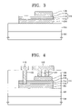
- FIGS. 1 through 4 are sectional views illustrating a method of manufacturing a capacitor of an analog semiconductor device with a multi-layer dielectric film according to an embodiment of the present invention.
- the capacitor includes a semiconductor substrate 100 on which a base structure including an analog circuit unit is formed, a lower electrode 104 , a lower dielectric film 112 , an intermediate dielectric film 114 , an upper dielectric film 116 , and an upper electrode 106 .
- a first interlayer insulator 102 is interposed between the semiconductor substrate 100 and the lower electrode 104 .
- the lower dielectric film 112 is formed on the lower electrode 104 and has a negative quadratic VCC.
- the intermediate dielectric film 114 is formed on the lower dielectric film 112 , and has a positive quadratic VCC.
- the upper dielectric film 116 is formed on the intermediate dielectric film 114 , and has a negative quadratic VCC.
- the upper electrode 106 is formed on the upper dielectric film 116 .
- Dielectric materials that have a negative quadratic VCC and are suitable for use in an analog capacitor include, for example, tantalum pentoxide (Ta 2 O 5 ), or silicon oxide (SiO 2 ).
- the SiO 2 material is particularly suitable for use in forming the lower dielectric film 112 and the upper dielectric film 116 according to the present invention since it is less likely to react with the upper electrode 106 and the lower electrode 104 than the Ta 2 O 5 material, and is excellent for preventing leakage current at high temperatures.
- SiO 2 has a more enhanced frequency efficiency of capacitor (FCC) parameter and a more enhanced temperature efficiency of capacitor (TCC) parameter than a conventional high-k dielectric material. Therefore, SiO 2 exhibits excellent dielectric characteristics for the dielectric material of the present invention.
- Dielectric materials that have a positive quadratic VCC and are suitable for use to form the intermediate dielectric film 114 include, for example, HfO 2 , ZrO 2 , or LaO 3 .
- the HfO 2 material has excellent VCC characteristics and is excellent for preventing leakage current.
- a base structure (not shown) is formed on a semiconductor substrate 100 using a conventional fabricating method.
- the base structure functions as an analog circuit.
- a first interlayer insulator 102 is deposited on the base structure, and then planarized.
- the first interlayer insulator 102 includes, for example, a single oxide layer or a plurality of oxide layers.
- a metal material is deposited on the first interlayer insulator 102 .
- the metal material operates as a lower electrode 104 of an analog capacitor.
- the lower electrode 104 comprises, for example, a material selected from Ti, TiN, Ta, TaN, Al, Cu, W, WN, Ir, IrO 2 , Ru and RuO 2 .
- the lower electrode 104 is connected to the base structure formed on the semiconductor substrate 100 , which is not shown in drawings.
- a NH 3 plasma treatment or a NH 3 heat treatment can be additionally performed at a temperature of 300-500° C. to improve characteristics of the resulting structure before the dielectric film 110 is formed thereon.
- a dielectric film 110 is formed on the entire upper surface of the lower electrode 104 .
- the dielectric film 110 is composed of a lower dielectric film 112 , an intermediate dielectric film 114 , an upper dielectric film 116 sequentially deposited.
- the lower dielectric film 112 and the upper dielectric film 116 are composed of a silicon oxide (SiO 2 ) material having a negative quadratic VCC parameter.
- the intermediate dielectric film 114 is composed of a material selected from HfO 2 , ZrO 2 , and LaO 3 . However, considering VCC characteristics, leakage current characteristics, and ease of forming a thin film, the use of HfO 2 is desirable for the intermediate dielectric film 114 .
- the dielectric film 110 is formed in situ using a plasma enhanced atomic layer deposition (PEALD) method. Formation of the dielectric film 110 by in-situ PEALD is more efficient than a method in which at least two of the dielectric films 112 , 114 , and 116 are deposited using other methods. In addition, since the three-layered dielectric film 110 is formed in-situ, contamination at the interfaces between the dielectric films 112 , 114 , and 116 is prevented and defects in the dielectric films 112 , 114 , and 116 can be minimized.
- PEALD plasma enhanced atomic layer deposition
- the lower dielectric film 112 and the upper dielectric film 116 are formed using PEALD, a catalytic method can be used. In such a case, the amount of impurities in the dielectric film 110 increases.
- PEALD used to form the lower dielectric film 104 and the upper dielectric film 106 HCDSO is used as a source at a chamber temperature of 200-300° C. and at a chamber pressure of 2-4 torr.
- Post-treatment can be additionally performed to decrease the impurities included in the lower dielectric film 112 and the upper dielectric film 116 .
- the post-treatment may comprise a plasma treatment or a heat treatment using a gas selected from NH 3 , O 2 , and O 3 .
- the post-treatment is performed, for example, at a temperature of 300-500° C.
- the metal material is deposited on the entire upper surface of the dielectric film 110 .
- the metal material operates as an upper electrode 106 .
- the upper electrode 106 is, for example, composed of a metal material selected from Ti, TiN, Ta, TaN, Al, Cu, W, WN, Ir, IrO 2 , Ru, and RuO 2 .
- the entire upper surface of electrode 106 is coated with a photoresist, patterning is performed, and then the upper electrode 106 is etched.
- the resultant structure is then coated with another photoresist, patterning is performed, and the dielectric film 110 and the lower electrode 104 are etched.
- the etched lower electrode 104 may have a larger surface area than the etched upper electrode 106 .
- a second interlayer insulator 108 is formed on the entire surface of the resultant semiconductor substrate, and planarized.
- the second interlayer insulator 108 may include a single oxide layer or a plurality of oxide layers.
- patterning is performed on the second interlayer insulator 108 .
- a plurality of contact holes 120 exposing the upper electrode 106 and a contact hole 122 exposing the lower electrode 104 are formed.
- the contact holes 120 exposing the upper electrode 106 are filled by contact plugs and the contact hole 122 exposing the lower electrode 102 is filled by a contact plug.
- Metal interconnections 118 are then formed, a first of which is connected to the contact plugs 120 for the upper electrode 106 and a second of which is connected to the contact plug for the lower electrode 104 .
- a capacitor of an analog semiconductor device includes an upper dielectric film, a lower dielectric film, and an intermediate dielectric film.
- the upper dielectric film and the lower dielectric film are composed of a material having a negative quadratic VCC
- the intermediate dielectric film is composed of a material having a positive quadratic VCC.
Abstract
Description
Q=C×V,
where C denotes an electrostatic capacitance, that is, a capacitance, and V is the voltage.
C(V)=C(0)×(a×V 2 +b×(V+1)),
where C(0) denotes the capacitance of the capacitor at an applied voltage of 0 V, a denotes a quadratic voltage coefficient of capacitance (VCC), and b denotes a linear VCC. Accordingly, in order to have a small VCC, a and b each should be 0 or nearly 0, and in particular, a should be nearly 0.
Claims (9)
Applications Claiming Priority (2)
| Application Number | Priority Date | Filing Date | Title |
|---|---|---|---|
| KR1020040051974A KR100630687B1 (en) | 2004-07-05 | 2004-07-05 | Capacitor of analog device having multi-layer dielectric and method forming the same |
| KR10-2004-0051974 | 2004-07-05 |
Publications (2)
| Publication Number | Publication Date |
|---|---|
| US20060017136A1 US20060017136A1 (en) | 2006-01-26 |
| US7407897B2 true US7407897B2 (en) | 2008-08-05 |
Family
ID=35656257
Family Applications (1)
| Application Number | Title | Priority Date | Filing Date |
|---|---|---|---|
| US11/173,624 Active US7407897B2 (en) | 2004-07-05 | 2005-07-01 | Capacitor of analog semiconductor device having multi-layer dielectric film and method of manufacturing the same |
Country Status (2)
| Country | Link |
|---|---|
| US (1) | US7407897B2 (en) |
| KR (1) | KR100630687B1 (en) |
Cited By (2)
| Publication number | Priority date | Publication date | Assignee | Title |
|---|---|---|---|---|
| US20090168297A1 (en) * | 2007-12-27 | 2009-07-02 | Taek-Seung Yang | Semiconductor device and method for manufacturing the same |
| US8432020B2 (en) | 2010-06-04 | 2013-04-30 | Sematech, Inc. | Capacitors, systems, and methods |
Families Citing this family (8)
| Publication number | Priority date | Publication date | Assignee | Title |
|---|---|---|---|---|
| KR100642635B1 (en) * | 2004-07-06 | 2006-11-10 | 삼성전자주식회사 | Semiconductor integrated circuit devices having a hybrid dielectric layer and methods of fabricating the same |
| KR100734144B1 (en) * | 2004-12-30 | 2007-06-29 | 동부일렉트로닉스 주식회사 | Method of fabricating MIM capacitor |
| FR2907592B1 (en) * | 2006-10-19 | 2008-12-26 | Commissariat Energie Atomique | THIN FILM CAPACITOR WITH HIGH STABILITY AND METHOD OF MANUFACTURE |
| KR20100041179A (en) | 2008-10-13 | 2010-04-22 | 매그나칩 반도체 유한회사 | Insulator, capacitor with the same and fabricating method thereof, and method for fabricating semiconductor device |
| US8901710B2 (en) * | 2013-02-27 | 2014-12-02 | International Business Machines Corporation | Interdigitated capacitors with a zero quadratic voltage coefficient of capacitance or zero linear temperature coefficient of capacitance |
| US20190229053A1 (en) * | 2018-01-22 | 2019-07-25 | United Microelectronics Corp. | Metal-insulator-metal capacitor structure and manufacturing method thereof |
| EP3796383A4 (en) * | 2019-07-26 | 2021-03-31 | Shenzhen Goodix Technology Co., Ltd. | Capacitance device and manufacturing method therefor |
| CN113629041A (en) * | 2020-05-09 | 2021-11-09 | 芯恩(青岛)集成电路有限公司 | MOS capacitor device and manufacturing method thereof |
Citations (20)
| Publication number | Priority date | Publication date | Assignee | Title |
|---|---|---|---|---|
| JPH0521710A (en) * | 1991-07-11 | 1993-01-29 | Hitachi Ltd | Semiconductor device |
| US6341056B1 (en) | 2000-05-17 | 2002-01-22 | Lsi Logic Corporation | Capacitor with multiple-component dielectric and method of fabricating same |
| US20030096473A1 (en) * | 2001-11-16 | 2003-05-22 | Taiwan Semiconductor Manufacturing Company | Method for making metal capacitors with low leakage currents for mixed-signal devices |
| KR20030079400A (en) | 2002-04-04 | 2003-10-10 | 동부전자 주식회사 | Capacitor of semiconductor device and method for manufacturing same |
| US20040002188A1 (en) | 2002-06-28 | 2004-01-01 | Chung Yi Sun | Method for fabricating MIM capacitor |
| US20040061157A1 (en) * | 2002-09-27 | 2004-04-01 | Masahiro Kiyotoshi | Semiconductor device |
| US20040072401A1 (en) * | 2002-10-10 | 2004-04-15 | Nec Electronics Corporation | Method for forming capacitor |
| US20040079980A1 (en) * | 2002-10-28 | 2004-04-29 | Kabushiki Kaisha Toshiba | Semiconductor device and method of manufacturing the same |
| US20040104420A1 (en) | 2002-12-03 | 2004-06-03 | International Business Machines Corporation | PREVENTION OF Ta2O5 MIM CAP SHORTING IN THE BEOL ANNEAL CYCLES |
| US20040232497A1 (en) * | 2001-12-14 | 2004-11-25 | Satoru Akiyama | Semiconductor device and method for manufacturing the same |
| US20050064236A1 (en) * | 2003-09-19 | 2005-03-24 | Lim Jung Wook | Inorganic thin film electroluminescent device and method for manufacturing the same |
| US6885056B1 (en) * | 2003-10-22 | 2005-04-26 | Newport Fab, Llc | High-k dielectric stack in a MIM capacitor and method for its fabrication |
| US20050110101A1 (en) * | 2003-08-29 | 2005-05-26 | Akio Kaneko | Semiconductor apparatus and method of manufacturing the semiconductor apparatus |
| US20050173778A1 (en) * | 2004-02-09 | 2005-08-11 | Won Seok-Jun | Analog capacitor and method of fabricating the same |
| US20050196915A1 (en) * | 2004-02-24 | 2005-09-08 | Jeong Yong-Kuk | Method of fabricating analog capacitor using post-treatment technique |
| US20050260357A1 (en) * | 2004-05-21 | 2005-11-24 | Applied Materials, Inc. | Stabilization of high-k dielectric materials |
| US20050269649A1 (en) * | 2001-10-12 | 2005-12-08 | Er-Xuan Ping | Even nucleation between silicon and oxide surfaces for thin silicon nitride film growth |
| US7091548B2 (en) | 2003-09-19 | 2006-08-15 | Samsung Electronics Co., Ltd. | Analog capacitor having at least three high-k-dielectric layers, and method of fabricating the same |
| US20060223276A1 (en) * | 2005-04-01 | 2006-10-05 | Chun-Yi Lin | MIM capacitor structure and fabricating method thereof |
| KR100873417B1 (en) | 2002-04-16 | 2008-12-11 | 페어차일드코리아반도체 주식회사 | Power semiconductor module having optimized DBC pattern and terminal structure |
-
2004
- 2004-07-05 KR KR1020040051974A patent/KR100630687B1/en active IP Right Grant
-
2005
- 2005-07-01 US US11/173,624 patent/US7407897B2/en active Active
Patent Citations (21)
| Publication number | Priority date | Publication date | Assignee | Title |
|---|---|---|---|---|
| JPH0521710A (en) * | 1991-07-11 | 1993-01-29 | Hitachi Ltd | Semiconductor device |
| US6341056B1 (en) | 2000-05-17 | 2002-01-22 | Lsi Logic Corporation | Capacitor with multiple-component dielectric and method of fabricating same |
| US20050269649A1 (en) * | 2001-10-12 | 2005-12-08 | Er-Xuan Ping | Even nucleation between silicon and oxide surfaces for thin silicon nitride film growth |
| US20030096473A1 (en) * | 2001-11-16 | 2003-05-22 | Taiwan Semiconductor Manufacturing Company | Method for making metal capacitors with low leakage currents for mixed-signal devices |
| US20040232497A1 (en) * | 2001-12-14 | 2004-11-25 | Satoru Akiyama | Semiconductor device and method for manufacturing the same |
| KR20030079400A (en) | 2002-04-04 | 2003-10-10 | 동부전자 주식회사 | Capacitor of semiconductor device and method for manufacturing same |
| KR100873417B1 (en) | 2002-04-16 | 2008-12-11 | 페어차일드코리아반도체 주식회사 | Power semiconductor module having optimized DBC pattern and terminal structure |
| KR20040001486A (en) | 2002-06-28 | 2004-01-07 | 주식회사 하이닉스반도체 | Method for forming mim capacitor |
| US20040002188A1 (en) | 2002-06-28 | 2004-01-01 | Chung Yi Sun | Method for fabricating MIM capacitor |
| US20040061157A1 (en) * | 2002-09-27 | 2004-04-01 | Masahiro Kiyotoshi | Semiconductor device |
| US20040072401A1 (en) * | 2002-10-10 | 2004-04-15 | Nec Electronics Corporation | Method for forming capacitor |
| US20040079980A1 (en) * | 2002-10-28 | 2004-04-29 | Kabushiki Kaisha Toshiba | Semiconductor device and method of manufacturing the same |
| US20040104420A1 (en) | 2002-12-03 | 2004-06-03 | International Business Machines Corporation | PREVENTION OF Ta2O5 MIM CAP SHORTING IN THE BEOL ANNEAL CYCLES |
| US20050110101A1 (en) * | 2003-08-29 | 2005-05-26 | Akio Kaneko | Semiconductor apparatus and method of manufacturing the semiconductor apparatus |
| US20050064236A1 (en) * | 2003-09-19 | 2005-03-24 | Lim Jung Wook | Inorganic thin film electroluminescent device and method for manufacturing the same |
| US7091548B2 (en) | 2003-09-19 | 2006-08-15 | Samsung Electronics Co., Ltd. | Analog capacitor having at least three high-k-dielectric layers, and method of fabricating the same |
| US6885056B1 (en) * | 2003-10-22 | 2005-04-26 | Newport Fab, Llc | High-k dielectric stack in a MIM capacitor and method for its fabrication |
| US20050173778A1 (en) * | 2004-02-09 | 2005-08-11 | Won Seok-Jun | Analog capacitor and method of fabricating the same |
| US20050196915A1 (en) * | 2004-02-24 | 2005-09-08 | Jeong Yong-Kuk | Method of fabricating analog capacitor using post-treatment technique |
| US20050260357A1 (en) * | 2004-05-21 | 2005-11-24 | Applied Materials, Inc. | Stabilization of high-k dielectric materials |
| US20060223276A1 (en) * | 2005-04-01 | 2006-10-05 | Chun-Yi Lin | MIM capacitor structure and fabricating method thereof |
Non-Patent Citations (1)
| Title |
|---|
| Won et al. ("Won") "Novel Plasma Enhanced Atomic Layer Deposition Technology for High-k Capacitor with EOT of 8.ANG. on Conventional Metal Electrode"; 2003 Symposium on VLSI Technology Digest of Technical Papers, 4-89114-035-6/03. * |
Cited By (2)
| Publication number | Priority date | Publication date | Assignee | Title |
|---|---|---|---|---|
| US20090168297A1 (en) * | 2007-12-27 | 2009-07-02 | Taek-Seung Yang | Semiconductor device and method for manufacturing the same |
| US8432020B2 (en) | 2010-06-04 | 2013-04-30 | Sematech, Inc. | Capacitors, systems, and methods |
Also Published As
| Publication number | Publication date |
|---|---|
| KR100630687B1 (en) | 2006-10-02 |
| KR20060003172A (en) | 2006-01-10 |
| US20060017136A1 (en) | 2006-01-26 |
Similar Documents
| Publication | Publication Date | Title |
|---|---|---|
| US7407897B2 (en) | Capacitor of analog semiconductor device having multi-layer dielectric film and method of manufacturing the same | |
| EP1517360B1 (en) | Analog capacitor and method of fabricating the same | |
| US7623338B2 (en) | Multiple metal-insulator-metal capacitors and method of fabricating the same | |
| US7897454B2 (en) | Metal-insulator-metal capacitor and fabrication method thereof | |
| US6777776B2 (en) | Semiconductor device that includes a plurality of capacitors having different capacities | |
| US7868421B2 (en) | Analog capacitor | |
| US6346746B1 (en) | Capacitor and electrode structures for a semiconductor device | |
| US20060006449A1 (en) | Semiconductor integrated circuit devices having a hybrid dielectric layer and methods of fabricating the same | |
| TWI401745B (en) | Semiconductor device and manufacturing method thereof | |
| US7554146B2 (en) | Metal-insulator-metal capacitor and method of fabricating the same | |
| US20070111496A1 (en) | Semiconductor device having dual stacked MIM capacitor and method of fabricating the same | |
| JP2004134579A (en) | Capacitor and its manufacturing method | |
| US20070026625A1 (en) | Method of fabricating metal-insulator-metal capacitor | |
| US20060154436A1 (en) | Metal-insulator-metal capacitor and a fabricating method thereof | |
| US7855431B2 (en) | Capacitor unit and method of forming the same | |
| JPH0563156A (en) | Manufacture of semiconductor device | |
| JP3943033B2 (en) | Capacitor and manufacturing method thereof | |
| US20060063290A1 (en) | Method of fabricating metal-insulator-metal capacitor | |
| US6677635B2 (en) | Stacked MIMCap between Cu dual damascene levels | |
| US7298019B2 (en) | Capacitor of semiconductor device and method of manufacturing the same | |
| US7067921B2 (en) | Method for fabricating a metal-insulator-metal capacitor in a semiconductor device | |
| EP0978881A2 (en) | Ferroelectric capacitor and its manufacturing method | |
| KR20040067012A (en) | Method for forming metal-insulator-metal capacitor of semiconductor device | |
| JP3967315B2 (en) | Capacitor element, semiconductor memory device and manufacturing method thereof | |
| KR20040107842A (en) | Semiconductor memory device having TiN lower electrode and method for manufacturing the same |
Legal Events
| Date | Code | Title | Description |
|---|---|---|---|
| AS | Assignment |
Owner name: SAMSUNG ELECTRONICS CO., LTD., KOREA, REPUBLIC OF Free format text: ASSIGNMENT OF ASSIGNORS INTEREST;ASSIGNORS:WON, SEOK-JUN;JEONG, YONG-KUK;KWON, DAE-JIN;AND OTHERS;REEL/FRAME:017174/0751 Effective date: 20050930 |
|
| FEPP | Fee payment procedure |
Free format text: PAYOR NUMBER ASSIGNED (ORIGINAL EVENT CODE: ASPN); ENTITY STATUS OF PATENT OWNER: LARGE ENTITY |
|
| STCF | Information on status: patent grant |
Free format text: PATENTED CASE |
|
| FPAY | Fee payment |
Year of fee payment: 4 |
|
| FPAY | Fee payment |
Year of fee payment: 8 |
|
| MAFP | Maintenance fee payment |
Free format text: PAYMENT OF MAINTENANCE FEE, 12TH YEAR, LARGE ENTITY (ORIGINAL EVENT CODE: M1553); ENTITY STATUS OF PATENT OWNER: LARGE ENTITY Year of fee payment: 12 |