US7400125B2 - Power supply circuit with series regulator - Google Patents
Power supply circuit with series regulator Download PDFInfo
- Publication number
- US7400125B2 US7400125B2 US11/328,418 US32841806A US7400125B2 US 7400125 B2 US7400125 B2 US 7400125B2 US 32841806 A US32841806 A US 32841806A US 7400125 B2 US7400125 B2 US 7400125B2
- Authority
- US
- United States
- Prior art keywords
- current
- circuit
- transistor
- voltage
- supply circuit
- Prior art date
- Legal status (The legal status is an assumption and is not a legal conclusion. Google has not performed a legal analysis and makes no representation as to the accuracy of the status listed.)
- Expired - Fee Related, expires
Links
- 238000001514 detection method Methods 0.000 claims description 10
- 238000010521 absorption reaction Methods 0.000 claims description 4
- 239000000047 product Substances 0.000 description 3
- 230000007423 decrease Effects 0.000 description 2
- 238000000034 method Methods 0.000 description 2
- 230000004048 modification Effects 0.000 description 2
- 238000012986 modification Methods 0.000 description 2
- 239000000758 substrate Substances 0.000 description 2
- 238000010276 construction Methods 0.000 description 1
- 230000002708 enhancing effect Effects 0.000 description 1
- 238000005728 strengthening Methods 0.000 description 1
- 239000013589 supplement Substances 0.000 description 1
- 230000007704 transition Effects 0.000 description 1
Images


Classifications
-
- G—PHYSICS
- G05—CONTROLLING; REGULATING
- G05F—SYSTEMS FOR REGULATING ELECTRIC OR MAGNETIC VARIABLES
- G05F1/00—Automatic systems in which deviations of an electric quantity from one or more predetermined values are detected at the output of the system and fed back to a device within the system to restore the detected quantity to its predetermined value or values, i.e. retroactive systems
- G05F1/10—Regulating voltage or current
- G05F1/46—Regulating voltage or current wherein the variable actually regulated by the final control device is DC
- G05F1/56—Regulating voltage or current wherein the variable actually regulated by the final control device is DC using semiconductor devices in series with the load as final control devices
- G05F1/575—Regulating voltage or current wherein the variable actually regulated by the final control device is DC using semiconductor devices in series with the load as final control devices characterised by the feedback circuit
Definitions
- the present invention relates to a power supply circuit with a series regulator.
- Power supply circuits which are required by almost all electronic apparatuses, can be categorized into a large number of types, one of which is a series-regulator type of power supply circuit.
- FIG. 1 exemplifies the electronic configuration of a series-regulator type of power supply circuit, which has typically been used by in-vehicle electronic equipment, such as ECU (Electronic Control Unit).
- ECU Electronic Control Unit
- the power supply circuit 1 shown in FIG. 1 has a supply circuit 4 (main power supply) to which a voltage VS is supplied from a battery 2 via an ignition (IG) switch 3 and a second supply circuit 5 (auxiliary power supply) to which the voltage VB is supplied directly from the battery 2 .
- Outputs of both supply circuits 4 and 5 are connected to a common output terminal 6 connected to a load circuit 7 .
- the input side of the supply circuit 4 is connected to a second load circuit 8 .
- the supply circuits 4 and 5 include main transistors 9 and 10 , respectively.
- the emitter and a base of each main transistor 9 ( 10 ) are connected to its input and output.
- This series-regulator type of power supply circuit 1 operates as follows.
- the supply circuits 4 and 5 both work, so that the voltage Vo at the output terminal 6 is stabilized to either one, which is higher than the other, of the target output voltage of the supply circuit 4 or that of the supply circuit 5 .
- the supply circuit 5 operates alone, so that the voltage Vo at the output terminal 6 is stabilized to the target output voltage of the supply circuit 4 .
- the base and collector of the PNP-type transistor 9 are inserted into the circuit in the forward direction. Therefore, though it depends on how the load circuit 8 is configured, it may happen that current flows in the backward direction from the supply circuit 5 to the load circuit 8 via the collector and base of the transistor 9 and the resistor 11 .
- a conceivable countermeasure is to place a diode between the ignition switch 3 and the transistor 9 .
- An object of the present invention is to provide, with due consideration to the drawbacks of the above conventional configuration, a series-regulator type of power supply circuit capable of preventing current flowing from an output terminal to an input terminal in the power supply circuit.
- the present invention provides a power supply circuit comprising: a transistor of which emitter and collector are connected to a power input terminal and a power output terminal, respectively; a voltage detection circuit configured to detect an output voltage at the power output terminal; a voltage control circuit connected to a base of the transistor and configured to control a base current of the transistor on the basis of both of the output voltage detected by the voltage detection circuit and a given target voltage; a resistor circuit placed to connect the base and the collector of the transistor; a current bypass circuit placed to connect the emitter and the base of the transistor and configured to bypass the transistor so that a bypass current flows through the current bypass circuit; and a current accepting circuit connected to the power output terminal and configured to accept a given amount of current from an output current passing the power output terminal by performing either absorption or discharge of the given amount of current, wherein the amount of current to be accepted is equal to or larger than an amount of the bypass current and a product of the amount of the bypass current and a resistance value of the resistance circuit is equal to or more than
- the resistor circuit is inserted between the base and the collector (not between the emitter and the base) of the transistor arranged between the power input/output terminals.
- This resistor circuit is able to fix a potential at the base to an amount equal to a potential at the collector, thereby strengthening resistance to noise.
- the emitter/base of the transistor provides a backward conjunction against the voltage applied to the power output terminal. And this circuitry provides no current path bypassing the emitter/base of the transistor. Accordingly, a backward current through the emitter/base of the transistor can be prevented, owing to the fact that the junction between the emitter/base of the transistor has a characteristic of cutting off the backward current.
- the current acceptance circuit is provided to avoid such an inconvenient situation.
- the current acceptance circuit has a capability of accepting current, the capability being equal to or higher than an amount of the bypass current.
- the current acceptance circuit thus absorbs or discharges the current that passes the resistance circuit. It is thus possible to make the current flow the resistance circuit even when there is no load, the current being required to suppress an unwanted swell in the output voltage.
- the output voltage can be controlled to the target voltage regardless of fluctuations in the amount of the load.
- the current acceptance circuit is composed of a constant-current circuit. This makes it possible that, even when the output voltage fluctuates, the current acceptance circuit is able to steadily accept (practically, absorb or discharge) the current passing the resistor circuit from the current bypass circuit. The output voltage can be prevented from increasing beyond control.
- the current acceptance circuit is composed of a resistor.
- the resistor an appropriately selected resistance value that is able to provide an amount of current equal to or higher than the bypass current, to an amount of the bypass current that flows under a condition where the output voltage is controlled to the target voltage, the output voltage can steadily be prevented from increasing beyond the target voltage.
- the current acceptance circuit is configured to absorb or discharge the acceptance current only when the current bypass circuit allows the bypass current to flow therethrough.
- the current acceptance circuit is able to stop its current acceptance operation. An unnecessary output current will not therefore be stopped, thus saving a consumed power in the power supply circuit, thus increasing efficiency in energy saving.
- the current bypass circuit is composed of a constant-current circuit.
- the constant-current circuit it is possible to provide a constant current that permits a product of the input voltage (which may fluctuate) and a resistance value of the resistor circuit to become an amount equal to or higher than a maximum difference between the input and output voltages. This prevents the output voltage from increasing over the target voltage in a reliable manner.
- auxiliary supply circuit configured to control the voltage at the power output terminal, independently of the voltage control performed by the main supply circuit.
- auxiliary supply circuit configured to control the voltage at the power output terminal, independently of the voltage control performed by the main supply circuit.
- FIG. 1 shows the electrical configuration of a conventional power supply circuit applied to an in-vehicle ECU
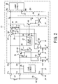
- FIG. 2 shows the electrical configuration of a power supply circuit, which is applied to an in-vehicle ECU, according to an embodiment of the present invention
- FIGS. 3A and 3B each show the electrical configurations of essential parts of the power supply circuits that were studied for achieving the power supply circuit according to the present invention.
- FIG. 4 shows an electrical configuration explaining a modification of the power supply circuit according to the present invention.
- FIGS. 2 to 3A and 3 B an embodiment of the present invention will now be described.
- FIG. 2 shows in detail a power supply circuit, which is particularly taken from the electrical configuration of an ECU (Electrical Control Unit) 21 for use in vehicles (cars).
- ECU Electronic Control Unit
- the ECU 21 has terminals 21 a to 21 c , as shown therein.
- One of the terminals, 21 a is electrically connected to a positive terminal of a battery 22 via an ignition (IG) switch 23 , while the other terminals 21 b and 21 c are electrically connected with the positive terminal and a negative terminal of the battery 22 , respectively.
- IG ignition
- the ECU 21 includes a frame (not shown), which incorporates a substrate (not shown). On the substrate, a power supply circuit 24 constructed in the form of an IC, a load circuit 25 that operates on power voltage supplied from the power supply circuit 24 , and a second load circuit 26 electrically connected with both the terminals 21 a and 21 c are provided.
- the load circuit 25 which is configured in the form of an IC different from the power supply circuit 24 , includes a microcomputer serving as a main device therein.
- This microcomputer is formed to have both a normal operation mode and a low-power-consumption operation mode, and can selectively be switched one from the other.
- consumed current is much lower to a large extent than that in the normal operation mode.
- the load circuit 26 includes a series circuit consisting of a switching element and a solenoid or relay coil, the switching element being subject to on/off control under a microcomputer.
- the power supply circuit 24 which has terminals 24 a to 24 c formed as IC terminals, is provided with a supply circuit 27 (serving as a main power supply) intervening between the terminals 24 a and 24 c and a second supply circuit 28 (serving as an auxiliary power supply) intervening between the terminals 24 b and 24 c .
- the IC input terminals 24 a and 24 b are coupled with the terminals 21 a and 21 b of the ECU 21 , respectively, while the output terminal 24 c and the ground terminal 24 d are coupled with power input terminals of the load circuit 25 , respectively.
- the supply circuits 27 and 28 are configured to have target output voltages of 5.0 [V] and 4.9 [V], respectively, and individually operate as a series regulator for controlling an output voltage Vo at the terminal 24 c in a constant voltage control manner.
- One of the supply circuits, 27 has a configuration described below.
- Both the terminals 24 a and 24 c are connected to an emitter and a collector of a PNP-type transistor 29 functioning as a main transistor.
- the base and the collector of the transistor 29 are connected to both terminals of a resistor 30 (composing a resistor circuit), while the base of the transistor 29 is electrically connected to the ground via the collector and emitter of a driving NPN-type transistor 31 .
- the terminal 24 c and the ground are connected to both terminals of a voltage dividing circuit 34 consisting of serially connected resistors 32 and 33 (composing a voltage detecting circuit).
- a resistor-connected point at which the voltage is divided is electrically connected to an inverting input terminal of the operational amplifier 35 that operates on the power from the terminal 24 a .
- the output terminal of this operational amplifier 35 is connected to the base of the foregoing driving transistor 31 , while a non-inverting input terminal of the operational amplifier 35 is connected to a reference voltage generating circuit 36 to output a reference voltage Vr 1 corresponding to a target output voltage (5.0 [V]).
- the transistor 31 and operational amplifier 35 compose a voltage control circuit.
- the emitter and the base of the transistor 29 are connected to a transistor 38 (composing a current bypass circuit), and the terminal 24 c and the ground are connected to a constant-current circuit 39 (composing a current accepting circuit).
- Each of the transistor 38 and the constant-current circuit 39 is driven by a bias voltage produced by a bias circuit 37 .
- the transistor 38 , a transistor 40 constructing the constant-current circuit 39 , and a transistor (not shown) constructing the bias circuit 37 have circuitry, in which all the bases thereof are connected together to a common base and all the emitters thereof are connected together to a common emitter.
- the constant-current circuit 39 is provided with a transistor 41 electrically inserted between the terminal 24 c and the ground a further transistor 42 electrically inserted between the transistor 40 and the ground, both the transistors 41 and 42 composing a current mirror circuit.
- This current mirror circuit configuration can be applied to both the transistors 38 and 40 .
- a current ratio between the current bypass circuit and the current accepting circuit can be fixed, thus making it possible to steadily set the current to be accepted to an amount equal to or more than the bypass current.
- both the transistors 41 and 4 Z are arranged close to each other to achieve the shortest wiring lengths therebetween so that a shift in the mirror ratio can be reduced.
- This arrangement for the shortest wiring length technique can also be applied to both the transistors 38 and 40 , which can reduce a shift in the mirror ratio as well.
- the remaining supply circuit 28 is configured in a similar way to the conventional.
- a PNP-type transistor 43 is placed so that its emitter and collector are electrically connected to the terminals 24 b and 24 c , while a resistor 44 intervenes between the emitter and the base of the transistor 43 .
- the base of the transistor 43 is grounded through the collector and emitter of a driving transistor 45 .
- each of the reference voltage generating circuits 36 and 50 is made with the use of, for example, a band-gap reference voltage circuit.
- the supply circuit 27 stops supplying the power, with the result that the other supply circuit 28 begins a constant-voltage operation, thus providing an output voltage Vo of 4.9 [V]. During this operation, a backward current from the collector of the transistor 29 to the emitter thereof will not flow, due to the reason described later.
- the microcomputer included in the load circuit 25 is able to sense an on/off operation of the ignition switch 23 . In response to a transition of the ignition switch 23 from its on-state to its off-state, the operation mode of the microcomputer will immediately shift from its normal operation mode to the low-power-consumption operation mode. Though the supply circuit 28 is set to a reduced current output capacity compared to that of the supply circuit 27 (whereby reducing power usage), it is still sufficient to supply power to the load circuit 25 .
- both of the supply circuits 27 and 28 are put into operation.
- the output voltage Vo is stabilized to 5.0 [V], which is higher one of the target output voltage of the supply circuit 27 or that of the supply circuit 2 .
- the supply circuit 28 of which target output voltage is 4.9 [V] turns the transistor 43 into its off-state, because the voltage error at the inputs of the operational amplifier 49 becomes a negative value.
- the microcomputer in the load circuit 25 shifts its operation mode from the low-power-consumption operation mode to the normal operation mode, so that the microcomputer is able to receive the power from the supply circuit 27 .
- FIGS. 3A and 3B each show the electrical configuration of essential parts of power supply circuits that were studied by the present inventors in the process for achieving the power supply circuit 24 ( FIG. 2 ) according to the present embodiment based on the conventional power supply circuit 1 ( FIG. 1 ).
- FIGS. 3A and 3B the identical components to those in FIG. 2 are represented by the same reference numbers.
- FIGS. 3A and 3B are not intended to show the formal power supply circuit, but introduced to explain only the significance of the presence of both the transistor 38 and constant-current circuit 39 in the power supply circuit 24 .
- the power supply circuit shown in FIG. 3A has identical circuitry to that of the conventional power supply circuit 1 except that the resistor 30 is inserted between the base and collector of the transistor 29 , not the emitter and base thereof.
- the constant voltage of 4.9 [V] outputted from the transistor 43 is applied as a backward voltage to the base/emitter junction of the transistor 29 .
- a backward current is prevented from flowing into the load circuit 26 via the transistor 29 .
- the potential at the base of the transistor 29 is fixed to an amount that is the same as a potential at the collector thereof, thereby enhancing resistance to noise.
- the power supply circuit shown in FIG. 3A has a difficulty as follows.
- the potential at the base of the transistor 29 becomes “VB ⁇ Vf (Vf: forward voltage),” so that a current proportional to “VB ⁇ Vf ⁇ Vo” flows through the resistor 30 .
- All of this current passing through the resistor 30 contributes to the base current of the transistor 29 independently of what state the transistor 31 takes. Because such base current will lead to a swell in the output voltage Vo, the output voltage Vo is obliged to exceed a target output voltage (i.e., 5.0 [V]).
- the power supply circuit shown in FIG. 3B is configured such that the transistor 38 is added to the circuitry described in FIG. 3A .
- This constant current I 1 corresponds to a bypass current according to the present invention.
- the current Ia passing through the resistor 30 under the on-state of the ignition switch 23 is supplied by the transistor 38 , not supplied as the base current of the transistor 29 . Accordingly, under conditions where a small amount of current flows into the load, the operational amplifier 35 is able to drive the transistor 31 so as to control the base current of the transistor 29 , with the result that the output voltage Vo can be limited to a constant voltage. During this control operation, any excessive amount of current “I 1 ⁇ Ia” is grounded via the transistor 31 . However, even this circuitry has a difficulty. In other words, when the output current from this power supply circuit becomes smaller than Ia, it is impossible to force the current to pass through the resistor 30 , thus causing a swell in the output voltage Vo.
- the power supply circuit 24 shown in FIG. 2 has further been improved in that the constant-current circuit 39 is added to the circuit shown in FIG. 3B .
- the constant-current circuit 39 is in charge of absorbing, from the output current of the transistor 29 , a constant amount of current I 2 which is equal to the current I 1 outputted by the transistor 38 .
- An alternative is that the current I 2 to be absorbed is higher than I 1 ; that is, the current I 2 is to satisfy the following formula (3): I2 ⁇ I1 (3).
- This absorption makes it possible to continue keeping the current Ia flowing through the resistor 30 , even when the current flowing from the power supply circuit 24 into the load circuit 25 is reduced. Accordingly, an unwanted swell in the output voltage Vo can be prevented reliably.
- the power supply circuit 24 of the present embodiment includes the two supply circuits 27 and 28 of which outputs are supplied to a common load, wherein the one supply circuit 27 is configured such that an input voltage supplied to the supply circuit 27 including the transistor 29 is stopped by turning off the ignition switch 23 , wherein the resistor 30 is inserted to be connected to the base and collector of the transistor 29 , instead of being connected to the emitter and base thereof.
- the emitter/base Junction of the transistor 29 prevents a backward current occurring on account of the output voltage Vo.
- the base potential of the transistor 29 is fixed to its collector potential, which enhances resistance to noise.
- the transistor 38 supplies the resistor 30 a current Ia, while the current-constant circuit 39 absorbs the current Ia from the output current of the transistor 29 .
- the output voltage Vo can be adjusted to a target output voltage (in this embodiment, 5.0 [V]) under constant-voltage control.
- the ECU on a vehicle operates on the power from the battery 22 .
- the ignition switch 23 is in its off-state, it is necessary to reduce consumed current (dark current) as much as possible through various countermeasures, such as a shift of the operation mode of the microcomputer to its low-power-consumption operation mode.
- both of the transistor 38 and the constant-current circuit 39 are added to the supply circuit 27 , such an addition will not increase the dark current, because both of the transistor 38 and the constant-current circuit 39 operate to output a constant current only when the ignition switch 23 is in its on-state.
- the current acceptance circuit can be configured with the use of a resistor 50 (refer to FIG. 4 ), in place of the foregoing constant-current circuit 39 that uses the current-constant circuit.
- the resistance Rb of the resistor 50 can be defined based on the following formula (4): Rb ⁇ 5.0 /I 1 (4).
- a switch circuit is connected to the resistor in series in such a manner that current is permitted to flow through the resistor only when the ignition switch 23 is in its on-state.
- the current bypassing circuit to be connected to the emitter and base of the transistor 29 is sufficient if the circuit has the characteristics of preventing a backward current flowing from the base of the transistor 29 to the emitter thereof and of being able to supply the current I 1 , so that the current bypassing circuit is not limited to a configuration that uses a constant-current circuit.
- the present invention can be applied to a series regulator that employs an NPN type of transistor 29 as the foregoing main transistor.
- NPN and PNP type transistors adopted in the power supply circuit 21 can be replaced by PNP and NPN type transistors, respectively, for the negative-voltage specification.
- N-MOS and P-MOS type transistors instead of the NPN and PNP type transistors.
Landscapes
- Engineering & Computer Science (AREA)
- Physics & Mathematics (AREA)
- Electromagnetism (AREA)
- General Physics & Mathematics (AREA)
- Radar, Positioning & Navigation (AREA)
- Automation & Control Theory (AREA)
- Continuous-Control Power Sources That Use Transistors (AREA)
Abstract
Description
I1≧Ia=(VB−Vf−5.0)/Ra (1),
wherein Ra is the resistance of the
I1≧Ia=(VB−5.0)/Ra (2).
I2≧I1 (3).
Rb≦5.0/I1 (4).
In this circuitry, it is preferred that a switch circuit is connected to the resistor in series in such a manner that current is permitted to flow through the resistor only when the
Claims (20)
Priority Applications (1)
| Application Number | Priority Date | Filing Date | Title |
|---|---|---|---|
| US11/328,418 US7400125B2 (en) | 2002-06-26 | 2006-01-10 | Power supply circuit with series regulator |
Applications Claiming Priority (4)
| Application Number | Priority Date | Filing Date | Title |
|---|---|---|---|
| JP2002-186016 | 2002-06-26 | ||
| JP2002186016A JP3829765B2 (en) | 2002-06-26 | 2002-06-26 | Power circuit |
| US10/602,605 US20040113599A1 (en) | 2002-06-26 | 2003-06-25 | Power supply circuit with series regulator |
| US11/328,418 US7400125B2 (en) | 2002-06-26 | 2006-01-10 | Power supply circuit with series regulator |
Related Parent Applications (1)
| Application Number | Title | Priority Date | Filing Date |
|---|---|---|---|
| US10/602,605 Continuation-In-Part US20040113599A1 (en) | 2002-06-26 | 2003-06-25 | Power supply circuit with series regulator |
Publications (2)
| Publication Number | Publication Date |
|---|---|
| US20060158164A1 US20060158164A1 (en) | 2006-07-20 |
| US7400125B2 true US7400125B2 (en) | 2008-07-15 |
Family
ID=31181491
Family Applications (2)
| Application Number | Title | Priority Date | Filing Date |
|---|---|---|---|
| US10/602,605 Abandoned US20040113599A1 (en) | 2002-06-26 | 2003-06-25 | Power supply circuit with series regulator |
| US11/328,418 Expired - Fee Related US7400125B2 (en) | 2002-06-26 | 2006-01-10 | Power supply circuit with series regulator |
Family Applications Before (1)
| Application Number | Title | Priority Date | Filing Date |
|---|---|---|---|
| US10/602,605 Abandoned US20040113599A1 (en) | 2002-06-26 | 2003-06-25 | Power supply circuit with series regulator |
Country Status (2)
| Country | Link |
|---|---|
| US (2) | US20040113599A1 (en) |
| JP (1) | JP3829765B2 (en) |
Families Citing this family (7)
| Publication number | Priority date | Publication date | Assignee | Title |
|---|---|---|---|---|
| JP4556795B2 (en) * | 2005-07-25 | 2010-10-06 | 株式会社デンソー | Power circuit |
| JP4783195B2 (en) * | 2006-04-18 | 2011-09-28 | パナソニック株式会社 | Buck converter |
| US7615976B2 (en) * | 2006-04-19 | 2009-11-10 | System General Corp. | Switching circuit of power converter having voltage-clipping device to improve efficiency |
| JP5492849B2 (en) * | 2011-09-20 | 2014-05-14 | 日立オートモティブシステムズ株式会社 | In-vehicle control device |
| CN103425057A (en) * | 2012-05-16 | 2013-12-04 | 鸿富锦精密工业(深圳)有限公司 | Switch circuit and electronic device with same |
| JP6417945B2 (en) * | 2015-01-07 | 2018-11-07 | ミツミ電機株式会社 | Power circuit |
| US10802517B1 (en) * | 2019-06-27 | 2020-10-13 | Texas Instruments Incorporated | Multi-mode voltage regulator |
Citations (12)
| Publication number | Priority date | Publication date | Assignee | Title |
|---|---|---|---|---|
| JPH0299413A (en) | 1988-10-06 | 1990-04-11 | Mazda Motor Corp | Suspension device for vehicle |
| US5302889A (en) | 1992-06-19 | 1994-04-12 | Honeywell Inc. | Voltage regulator |
| US5596465A (en) | 1994-03-11 | 1997-01-21 | Fujitsu Limited | Overcurrent protection circuit for a dc-to-dc converter |
| US5892353A (en) * | 1996-07-25 | 1999-04-06 | Rohm Co. Ltd. | Power supply apparatus |
| US5932996A (en) | 1998-04-28 | 1999-08-03 | Hewlett-Packard Co. | Low cost current mode control switching power supply without discrete current sense resistor |
| JP2000155619A (en) | 1998-11-20 | 2000-06-06 | Denso Corp | Constant voltage power supply unit |
| JP2001209441A (en) | 2000-01-26 | 2001-08-03 | Hokuriku Electric Ind Co Ltd | Circuit for constant-voltage power supply |
| US6812682B2 (en) | 2001-12-06 | 2004-11-02 | Matsushita Electric Industrial Co., Ltd. | Switching power supply unit and semiconductor device for switching power supply |
| US6850047B2 (en) | 2002-10-30 | 2005-02-01 | Denso Corporation | Switching regulator and power supply using the same |
| US6984966B2 (en) * | 2003-09-05 | 2006-01-10 | Shindengen Electric Manufacturing Co., Ltd. | Switching power supply |
| US7002324B2 (en) * | 2002-03-15 | 2006-02-21 | Tdk Corporation | Switching power supply control circuit and switching power supply using same |
| US20060255785A1 (en) * | 2005-05-16 | 2006-11-16 | Sharp Kabushiki Kaisha | Stabilized DC power supply circuit |
-
2002
- 2002-06-26 JP JP2002186016A patent/JP3829765B2/en not_active Expired - Fee Related
-
2003
- 2003-06-25 US US10/602,605 patent/US20040113599A1/en not_active Abandoned
-
2006
- 2006-01-10 US US11/328,418 patent/US7400125B2/en not_active Expired - Fee Related
Patent Citations (12)
| Publication number | Priority date | Publication date | Assignee | Title |
|---|---|---|---|---|
| JPH0299413A (en) | 1988-10-06 | 1990-04-11 | Mazda Motor Corp | Suspension device for vehicle |
| US5302889A (en) | 1992-06-19 | 1994-04-12 | Honeywell Inc. | Voltage regulator |
| US5596465A (en) | 1994-03-11 | 1997-01-21 | Fujitsu Limited | Overcurrent protection circuit for a dc-to-dc converter |
| US5892353A (en) * | 1996-07-25 | 1999-04-06 | Rohm Co. Ltd. | Power supply apparatus |
| US5932996A (en) | 1998-04-28 | 1999-08-03 | Hewlett-Packard Co. | Low cost current mode control switching power supply without discrete current sense resistor |
| JP2000155619A (en) | 1998-11-20 | 2000-06-06 | Denso Corp | Constant voltage power supply unit |
| JP2001209441A (en) | 2000-01-26 | 2001-08-03 | Hokuriku Electric Ind Co Ltd | Circuit for constant-voltage power supply |
| US6812682B2 (en) | 2001-12-06 | 2004-11-02 | Matsushita Electric Industrial Co., Ltd. | Switching power supply unit and semiconductor device for switching power supply |
| US7002324B2 (en) * | 2002-03-15 | 2006-02-21 | Tdk Corporation | Switching power supply control circuit and switching power supply using same |
| US6850047B2 (en) | 2002-10-30 | 2005-02-01 | Denso Corporation | Switching regulator and power supply using the same |
| US6984966B2 (en) * | 2003-09-05 | 2006-01-10 | Shindengen Electric Manufacturing Co., Ltd. | Switching power supply |
| US20060255785A1 (en) * | 2005-05-16 | 2006-11-16 | Sharp Kabushiki Kaisha | Stabilized DC power supply circuit |
Non-Patent Citations (1)
| Title |
|---|
| Notification of Reasons for Rejection from Japanese Patent Office issued on Mar. 22, 2006 for the corresponding Japanese patent application No. 2002-186016. |
Also Published As
| Publication number | Publication date |
|---|---|
| JP2004030266A (en) | 2004-01-29 |
| US20060158164A1 (en) | 2006-07-20 |
| US20040113599A1 (en) | 2004-06-17 |
| JP3829765B2 (en) | 2006-10-04 |
Similar Documents
| Publication | Publication Date | Title |
|---|---|---|
| US7071664B1 (en) | Programmable voltage regulator configurable for double power density and reverse blocking | |
| US8054605B2 (en) | Power supply controller | |
| US7586296B2 (en) | Power supply apparatus | |
| US7068485B2 (en) | Multi-output electric power source device and vehicle-mounted electronic control device | |
| US6804096B2 (en) | Load driving circuit capable of raised accuracy detection of disconnection and short circuit of the load | |
| US8994220B2 (en) | Vehicle-mounted electronic control device | |
| US7400125B2 (en) | Power supply circuit with series regulator | |
| JP4107052B2 (en) | Multi-output power supply | |
| JP3747618B2 (en) | Power circuit | |
| US4555742A (en) | Short detection circuit and method for an electrical load | |
| US6876180B2 (en) | Power supply circuit having a start up circuit | |
| JP3700816B2 (en) | Solenoid drive | |
| JP2865133B2 (en) | Stabilized power supply circuit | |
| US20020057583A1 (en) | Switching power supply unit and electronic apparatus using the same | |
| JP2005050055A (en) | Power supply device | |
| JPH0632186A (en) | On-vehicle power source control device | |
| JP3232739B2 (en) | Switch ON detection circuit | |
| US6337587B2 (en) | Circuit arrangement for driving a load by two transistors | |
| WO2021166389A1 (en) | Semiconductor integrated circuit for power supply, and power supply system | |
| US20060119414A1 (en) | Gate drive circuit for semiconductor device | |
| US20070146016A1 (en) | Signal output circuit and power source voltage monitoring device using the same | |
| JP3468119B2 (en) | Constant voltage power supply circuit | |
| JP3446593B2 (en) | Power circuit | |
| JP4172076B2 (en) | Constant voltage power supply | |
| JP2020137137A (en) | Clamp circuit |
Legal Events
| Date | Code | Title | Description |
|---|---|---|---|
| AS | Assignment |
Owner name: DENSO CORPORATION, JAPAN Free format text: ASSIGNMENT OF ASSIGNORS INTEREST;ASSIGNORS:KOJIMA, AKIO;NAGATA, JUNICHI;REEL/FRAME:017945/0394 Effective date: 20060411 |
|
| STCF | Information on status: patent grant |
Free format text: PATENTED CASE |
|
| FPAY | Fee payment |
Year of fee payment: 4 |
|
| FEPP | Fee payment procedure |
Free format text: PAYOR NUMBER ASSIGNED (ORIGINAL EVENT CODE: ASPN); ENTITY STATUS OF PATENT OWNER: LARGE ENTITY |
|
| FPAY | Fee payment |
Year of fee payment: 8 |
|
| FEPP | Fee payment procedure |
Free format text: MAINTENANCE FEE REMINDER MAILED (ORIGINAL EVENT CODE: REM.); ENTITY STATUS OF PATENT OWNER: LARGE ENTITY |
|
| LAPS | Lapse for failure to pay maintenance fees |
Free format text: PATENT EXPIRED FOR FAILURE TO PAY MAINTENANCE FEES (ORIGINAL EVENT CODE: EXP.); ENTITY STATUS OF PATENT OWNER: LARGE ENTITY |
|
| STCH | Information on status: patent discontinuation |
Free format text: PATENT EXPIRED DUE TO NONPAYMENT OF MAINTENANCE FEES UNDER 37 CFR 1.362 |
|
| FP | Lapsed due to failure to pay maintenance fee |
Effective date: 20200715 |