US7342969B2 - Signaling with multiple clocks - Google Patents
Signaling with multiple clocks Download PDFInfo
- Publication number
- US7342969B2 US7342969B2 US10/629,325 US62932503A US7342969B2 US 7342969 B2 US7342969 B2 US 7342969B2 US 62932503 A US62932503 A US 62932503A US 7342969 B2 US7342969 B2 US 7342969B2
- Authority
- US
- United States
- Prior art keywords
- signals
- data
- multiple potential
- reference times
- digital
- Prior art date
- Legal status (The legal status is an assumption and is not a legal conclusion. Google has not performed a legal analysis and makes no representation as to the accuracy of the status listed.)
- Expired - Fee Related, expires
Links
Images


Classifications
-
- H—ELECTRICITY
- H04—ELECTRIC COMMUNICATION TECHNIQUE
- H04L—TRANSMISSION OF DIGITAL INFORMATION, e.g. TELEGRAPHIC COMMUNICATION
- H04L7/00—Arrangements for synchronising receiver with transmitter
-
- H—ELECTRICITY
- H04—ELECTRIC COMMUNICATION TECHNIQUE
- H04L—TRANSMISSION OF DIGITAL INFORMATION, e.g. TELEGRAPHIC COMMUNICATION
- H04L25/00—Baseband systems
- H04L25/38—Synchronous or start-stop systems, e.g. for Baudot code
- H04L25/40—Transmitting circuits; Receiving circuits
- H04L25/49—Transmitting circuits; Receiving circuits using code conversion at the transmitter; using predistortion; using insertion of idle bits for obtaining a desired frequency spectrum; using three or more amplitude levels ; Baseband coding techniques specific to data transmission systems
- H04L25/493—Transmitting circuits; Receiving circuits using code conversion at the transmitter; using predistortion; using insertion of idle bits for obtaining a desired frequency spectrum; using three or more amplitude levels ; Baseband coding techniques specific to data transmission systems by transition coding, i.e. the time-position or direction of a transition being encoded before transmission
-
- H—ELECTRICITY
- H04—ELECTRIC COMMUNICATION TECHNIQUE
- H04L—TRANSMISSION OF DIGITAL INFORMATION, e.g. TELEGRAPHIC COMMUNICATION
- H04L25/00—Baseband systems
- H04L25/02—Details ; arrangements for supplying electrical power along data transmission lines
- H04L25/08—Modifications for reducing interference; Modifications for reducing effects due to line faults ; Receiver end arrangements for detecting or overcoming line faults
- H04L25/085—Arrangements for reducing interference in line transmission systems, e.g. by differential transmission
-
- H—ELECTRICITY
- H04—ELECTRIC COMMUNICATION TECHNIQUE
- H04L—TRANSMISSION OF DIGITAL INFORMATION, e.g. TELEGRAPHIC COMMUNICATION
- H04L7/00—Arrangements for synchronising receiver with transmitter
- H04L7/0008—Synchronisation information channels, e.g. clock distribution lines
-
- H—ELECTRICITY
- H04—ELECTRIC COMMUNICATION TECHNIQUE
- H04L—TRANSMISSION OF DIGITAL INFORMATION, e.g. TELEGRAPHIC COMMUNICATION
- H04L7/00—Arrangements for synchronising receiver with transmitter
- H04L7/02—Speed or phase control by the received code signals, the signals containing no special synchronisation information
Definitions
- This description relates to signaling with multiple clocks.
- this chip-to-chip communication is often implemented as a number of parallel data interconnects that comprise a bus 22 .
- digital data is represented as the timing of pulses carried on each interconnect with reference to one or more clock signals that are carried on a clock line 24 provided by a common source 26 .
- Forwarded clock signals are typically routed in a manner similar to that of the data signals they accompany.
- the signals between the input/output (I/O) transceivers 28 and 30 must traverse channel segments both on the IC's 32 and between them 34 that have impairments and are, for practical low cost channel components, less capable of supporting the required data transmission rates than are the transceiver circuits themselves.
- impairments include dispersion, crosstalk, loss, reflections due to mismatch, lowpass filtering effects of the channel and other factors that together impose an upper limit on the throughput of the physical link (boards, packages and circuit) at a given maximum Bit Error Rate (BER).
- BER Bit Error Rate
- ISI inter-symbol interference
- These impairments to the capacity of the physical channel can be mitigated somewhat by use of higher performance components and circuit board materials, which incur greater cost. Adding additional data lines to a bus will also add cost in terms of both power and board routing space.
- modulation can be used in place of conventional binary signaling to yield an advantage in data throughput by making greater use of the available channel bandwidth.
- Practical digital wide-band modulation includes pulse width modulation (PWM), phase modulation (PM), amplitude modulation (AM), and risetime modulation.
- PWM pulse width modulation
- PM phase modulation
- AM amplitude modulation
- risetime modulation Many other techniques for improving a channel's binary throughput performance exist including such strategies as transmit and/or receive side equalization and echo cancellation.
- Return-to-reference or non-return-to-reference differential signaling is commonly used. Many of these signaling schemes may be layered to form phase and amplitude modulation together, for example.
- Active elements capable of generating and resolving signal transitions to within narrow time increments can be used in transmitters and receivers in order to implement PM, PWM, and similar modulation schemes in which the locations of signal transitions are varied in time with respect to an embedded or parallel time reference.
- digital data may be encoded in terms of a time difference 40 between a signal transition 42 and the precisely known time of occurrence of a transition 44 of a reference clock.
- a transition will be assumed to be either a change in level, such as is used in level-based NRZ signaling; or a pulse, such as that used in RZ signaling.
- timing resolution that is, the precision with which the time difference 40 can be determined.
- a system that relies on discrimination of the phase of a transition with respect to the phase of a reference transition to achieve time resolution will accumulate temporal measurement variations throughout the duration of the interval 40 separating the signal transition from its timing reference transition. This phenomenon is described as jitter integration. Sources of jitter may include power supply variations or simultaneous switching of other active circuit elements, for example. If the integrated jitter is too high, ambiguity or errors in the classification of the arrival time of a transition may result. It is expected that the jitter will vary over time, being both additive and subtractive, with the greatest potential jitter integration occurring over long timing intervals. One must consider the possibility that all jitter contributions will be additive when setting the worst-case jitter margin.
- two time references will accumulate jitter with respect to one another as they pass through dissimilar physical segments, typically active elements, in a circuit. Signals that emanate from a common source are considered to be identical, and initially have zero jitter with respect to one another. It is an accepted practice to assume that signals that pass through similar adjacent circuit elements that share the same power supply will jitter together with high correlation and with little net difference in their relative phase. The jitter statistics of a signal will be preserved as it transits passive elements comprising similar physical channels, and may increase further due to other sources such as electromagnetic interference (EMI), and crosstalk.
- EMI electromagnetic interference
- jitter integration increases as the time difference 40 separating the transitions of a data line and adjacent reference clock transitions increase. Reducing a data channel's time difference 40 reduces the error in phase measurement caused by jitter accumulation.
- the reference clock signal is generated at a rate that is sufficiently high that the inaccuracy in measured delay is minimized.
- the clock transitions 44 may also be aligned with data line transitions 42 to further reduce relative timing errors.
- the clock reference is then forwarded with the data signals in the bus using matched circuit and board structures. Since the physical channel frequently serves to limit the frequency spectrum content of transmitted signals, a limit is often reached in the rate that this clock can be run. Another limiting factor on the clock is electromagnetic EMI emissions, which often increase with frequency and must meet regulatory and system requirements related to EMI pickup of other system components.
- the modulator and demodulator circuits can use the nearest reference clock transition as a timing reference, thereby minimizing the time-distance from the reference and resulting jitter integration.
- phase modulation scheme data line transitions are permitted over a continuous range of phase positions, with respect to the reference clock. This allows an arbitrarily large symbol set that could provide infinite data throughput.
- the practical barrier to achieving this throughput is the limited precision that is possible in localizing a transition's discrete location in time, largely due to circuit and ISI jitters.
- Using a single clock reference with a phase modulation scheme having several phase slots means that the time distance of transitions of the data line to those of the clock will vary, depending on which modulation state was generated.
- a designer typically assumes a conservative, worst-case jitter margin that ensures that jitter does not lead to mis-classification (bit error) of the phase of an incoming data signal.
- FIG. 1 is a block diagram of circuits connected by a communication bus.
- FIG. 2 shows a time difference between data and clock transitions.
- FIG. 3 is a timing diagram showing multiple clocks with a phase skew.
- FIG. 4 is a schematic of a data symbol showing the slot range.
- FIG. 5 is a plot of the timing uncertainty due to jitter.
- FIG. 6 shows a single clock phase modulation scheme.
- FIG. 7 is a block diagram of a single clock modulator.
- FIG. 8 is a block diagram of a single clock demodulator
- FIG. 9 shows a dual clock phase modulation scheme.
- FIG. 10 is a block diagram of a dual clock modulator.
- FIG. 11 is a block diagram of a dual clock demodulator.
- FIG. 12 is a plot of a square wave.
- FIG. 13 is a plot of a piecewise linear waveform.
- FIG. 14 shows plots of harmonic power spectra.
- FIG. 15 shows plots of harmonic power spectra.
- FIG. 16 is a block diagram of a single clock modulator.
- FIG. 17 is a block diagram of a dual clock modulator.
- FIG. 18 is a block diagram of a single clock demodulator.
- FIG. 19 is a block diagram of a dual clock demodulator
- clocks may be used to improve the timing resolution of, for example, phase and pulse-width modulated signals.
- the clock signals can be derived from the same source, but can have phases that are skewed with respect to one another by a pre-designed amount 50 , as shown in FIG. 3 .
- the modulator circuit can then reference the data transitions to the clock signal whose edge is closest to that transition. Since there are more clock transitions, the interval of time from a data signal transition to the nearest clock transition can be reduced. Jitter integration, which increases with the temporal distance between a data transition and its reference clock transition, will also be reduced resulting in an overall reduction in circuit jitter. This leads to a higher achievable bandwidth.
- the addition of more than one clock signal might require the sacrifice of an equivalent data line for carrying each additional clock signal, due to conductor routing constraints.
- the aggregate reduction in bus bandwidth caused by the loss of one (or more) data lines will be offset, under certain circumstances, by the overall increase in data rate per data line that is made possible by the improved jitter tracking bandwidth. For example, with ten data lines, the increase in bandwidth would only have to be on the order of 10% to just compensate for a single extra clock line. As the number of data lines increases the impact of sacrificing data lines in exchange for extra clock lines is even smaller, resulting in more modest increases in data rates to compensate.
- a digital signal is any signal onto which digital data (e.g., bit sequences) has been encoded using any one or combination of a variety of modulation techniques (e.g., PWM, PM, AM, PAM, QAM) that define a set of symbols.
- modulation techniques e.g., PWM, PM, AM, PAM, QAM
- the bandwidth of a data line will increase with the number of bits that can be encoded per symbol, which depends not only on the circuit jitter, but also by the accuracy of the timing circuits.
- the additional on-die area consumed by the circuits required to exploit the additional timing sources may also limit the number of clock and data lines. For a complete optimization of the aggregate bandwidth one should also factor in such things as the quality of the channel, which can affect the BER and the minimum symbol period.
- a system may use digital data encoded on symbols 200 that have transitions occurring only at predetermined possible time delays from reference clock transitions 202 , the time delays thus comprising a set of phase slots 204 , as shown in FIG. 4 .
- the time delays thus comprising a set of phase slots 204 , as shown in FIG. 4 .
- Timing budget allotted for these and other sources of timing variation is defined to be TBO (timing budget other than clock jitter).
- TBO timing budget other than clock jitter
- the truncation can be chosen to support a target maximum BER, such as 10 ⁇ 16 . Once truncated, the distributions may be added together to produce a worst-case result. Timing variation due to ISI may be modeled by a boundary function distribution that may be computed using peak distortion analysis.
- n max ⁇ ( 1 + j - 2 ⁇ TBO ) 2 ⁇ j ⁇ .
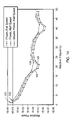
- FIG. 5 depicts the mounting effects of jitter on a system intended to have thirty-one equally spaced phase slots between adjacent clock transitions, shown in the upper trace 62 .
- FIG. 6 consider another implementation of a system that uses an 800 pico-second (ps) base pulse, modulated with four equally spaced 400 ps phase slots on both the rising 80 and falling 82 transitions.
- an 800 ps spacer 84 is required at the end of the symbol to minimize inter-symbol interference (ISI), thus forming a 4000 ps symbol frame 86 .
- ISI inter-symbol interference
- two transitions must occur in the symbol, one in any of the four leading slots 80 (encoding two bits of data) and another in the trailing group of four slots 82 (encoding another two bits of data). Each symbol provides four bits of data.
- FIG. 6 shows the time distances to the nearest reference transitions when there is only a single symmetric clock pulse 88 whose transitions are positioned to minimize jitter integration of the worst-case data transitions. It is assumed that the clock and data lines accumulate jitter at the same rate. It can be seen from FIG. 6 that the worst-case modulator jitter integration time is 600 ps, or 11 ⁇ 2 unit intervals, which forces circuit designers to consume a larger share of their jitter budget to account for this. More jitter will be incurred during demodulation.
- FIG. 7 A conceptual diagram of an implementation of the single-clock modulation scheme is shown in FIG. 7 , where a unit delay is equal to 400 ps using the timing assumed in FIG. 6 .
- the clock out 92 can be forwarded using circuit structures that are matched to the structures used for the modulated data out 94 to account for time delays due to conductor routing constraints (e.g., using de-skew circuitry) such that their relative delay is as shown in FIG. 7 .
- the first and fourth transitions are separated from the clock reference by 11 ⁇ 2 unit delays.
- the second and third transitions are separated from the clock reference by 1 ⁇ 2 unit delays.
- the digital data in 96 determines which of the inputs to the MUX 98 is selected to drive the modulated data out 94 .
- the corresponding single-clock demodulator is shown in FIG. 8 .
- An arbiter 101 determines which of transitions on its inputs occurs first. If arbiter 101 determines a data transition occured first then slot 1 is detected. Similarly, if arbiter 102 determines a data transition occurred first then slot 2 is detected, and if arbiter 103 determines a data transition occurred first then slot 3 is detected.
- the demodulator circuit uses delays where necessary to place the clock transition in the center of two possible adjacent data transitions (the center of the received “eye”). Therefore, the demodulator imparts another unit interval of jitter integration, for a total jitter integration of 21 ⁇ 2 unit intervals.
- the arrival of a data transition in the fourth slot may be assumed for modulation schemes with guaranteed transitions as in the example shown in FIG. 7 ; therefore no arbiter is used to detect slot 4 .
- the symbol mapper 104 then uses the outputs of the arbiters to generate the decoded data out 105 .
- the modulation scheme is shown above in FIG. 9 is identical to the one in FIG. 6 , except for the clocking. Two clocks are used, which are aligned with slots 2 and 3 . From FIG. 10 it can be seen that the jitter integration times are reduced to one unit interval at the modulator. An additional 1 ⁇ 2 unit interval of jitter integration is accrued at the demodulator, as shown in FIG. 11 . This results in a total accumulated jitter integration time of 11 ⁇ 2 unit intervals, 60% of the single clock case. Again, slot 4 is assumed by default in the symbol mapper 110 .
- Adding a second clock reference to the bus as shown reduces the jitter integration, but even greater gains can be obtained.
- Adding a third clock to the example shown would reduce the jitter integration time to 1 ⁇ 2 of a unit interval, 33% of the two clock case, and 20% of the single clock case.
- Transmission of digital data using multiple phase-shifted clocks can also increase the performance of amplitude-modulated signals (e.g., 2-PAM which is simply binary amplitude-modulation) through its effect on EMI.
- Clocks unlike data, have regular alternately high/low amplitude patterns corresponding to time-invariant emission spectra and are therefore worse contributors to EMI emission than are the corresponding data lines, whose emission spectra are typically more distributed.
- Multiple clocks operating at frequencies that are lower than that of a single, higher-speed clock can provide equivalent timing references for amplitude-modulated signals while reducing the emissions spectrum that causes EMI.
- Phase-modulated signals also benefit from reduced EMI of multiple phase-shifted lower frequency clocks, in addition to the increase in bandwidth from lower jitter integration as described above.
- a periodic signal can be expressed as a sum of a number of sinusoidal frequency components using a Fourier series.
- the frequencies of the components are multiples of the fundamental frequency 1/T, where T is the period of the signal.
- the amplitude of each constituent component is determined by the shape of the waveform.
- a digital clock signal is often conveniently represented schematically as a square wave, as shown in FIG. 12 .
- the Fourier series representation of a pure square wave having a period T is
- A is the amplitude of the waveform
- ⁇ 0 is its fundamental frequency, which is related to the period by
- ⁇ 0 2 ⁇ ⁇ T .
- High-speed clock signals seldom behave like perfect square waves. Instead, they have finite rise-times, fall-times, and plateaus that are often each approximated as being linear, forming the piecewise linear waveform shown in FIG. 13 , with period T, rise-time R, and fall-time F. If the rise and fall times are taken as being equal, the Fourier series takes the form:
- the plots in FIG. 14 show the relative magnitudes of the power spectra of one half-speed clock 124 , two half-speed clocks 126 , and one full-speed clock 128 . While the half-speed pair have a fundamental frequency component with a combined power 120 that is twice that 122 of the single full-speed clock, for relative frequencies above the full-speed frequency, two half-speed clocks 126 have lower power, and therefore lower EMI emissions, than one full-speed clock 128 .
- FIG. 16 shows an exemplary transmitter modulator circuit for binary amplitude-modulation using one full-speed clock.
- a flip-flop (FF) 150 is used as a synchronization circuit to synchronize to the clock in 152 .
- a corresponding FF compensation circuit 154 logically a buffer, is used to match the jitter integration of the forwarded clock path to the jitter integration of the data path.
- An equalization circuit 155 is used to compensate for gain variation over the spectrum of the modulated data signal that, if left uncompensated, could lead to distortion and a higher BER.
- FIG. 17 shows an exemplary transmitter modulator circuit for binary amplitude-modulation modified to use two half-speed clocks shifted in phase by 90 degrees.
- a flip-flop 160 that clocks data in response to the edges of both the zero phase clock 162 and the 90 degree phase shifted clock 164 , is used to synchronize the data to the two forwarded clocks.
- a first FF Compensation block 166 and a second FF Compensation block 168 are used to match the jitter integration of the clock paths to the jitter integration of the data path.
- FIG. 18 shows an exemplary receiver demodulator circuit corresponding to the modulator circuit of FIG. 16 , using the full-speed clock.
- the timing block 170 provides clock amplification and de-skew circuitry to align the clock to the data.
- This block 170 includes a delay locked loop (DLL), a phase interpolator, a level converter, and receiver control logic.
- a phase-1 clock 172 and a phase-2 clock 174 are half-speed clocks with a relative 90 phase shift generated from the clock in 176 by the timing block 170 . Interleaved circuit components are then used do separately decode even and odd modulated data symbols.
- DLL delay locked loop
- phase-1 clock 172 is used by the sampler/equalizer 178 in order to decode even modulated data symbols
- phase-2 clock 174 is used by the sampler/equalizer 180 in order to decode odd modulated data symbols.
- Even data from a first decision circuit 182 is interleaved with odd data from a second decision circuit 184 by a synchronizer 186 to produce decoded data out 188 .
- FIG. 19 shows an exemplary receiver demodulator circuit corresponding to the modulator circuit of FIG. 17 , using two half-speed clocks.
- the operation of this demodulator circuit is similar to the operation of the circuit in FIG. 18 .
- the timing block 190 also provides clock amplification and de-skew circuitry, and includes a phase interpolator, a level converter, and receiver control logic. However, in this two clock demodulator circuit, the timing block 190 generates the phase-1 clock 196 from the zero degree clock 192 , and the phase-2 clock 198 from the 90 degree clock 194 .
Landscapes
- Engineering & Computer Science (AREA)
- Computer Networks & Wireless Communication (AREA)
- Signal Processing (AREA)
- Power Engineering (AREA)
- Physics & Mathematics (AREA)
- Spectroscopy & Molecular Physics (AREA)
- Dc Digital Transmission (AREA)
- Synchronisation In Digital Transmission Systems (AREA)
- Mechanical Light Control Or Optical Switches (AREA)
- Financial Or Insurance-Related Operations Such As Payment And Settlement (AREA)
- Train Traffic Observation, Control, And Security (AREA)
Abstract
Description
(n−1)(1+j)+TBO=n(1−j)−TBO
which can be solved for nmax the most distant resolvable slot
This indicates that if equally spaced slots are chosen, there is a limit on the number of discrete phase positions that may reference a particular clock transition, regardless of the slot size, for a given linear jitter.
where A is the amplitude of the waveform, and ω0 is its fundamental frequency, which is related to the period by
where RTF is defined as being the fraction of the overall period consumed by the rise time,
Claims (33)
Priority Applications (8)
| Application Number | Priority Date | Filing Date | Title |
|---|---|---|---|
| US10/629,325 US7342969B2 (en) | 2003-07-28 | 2003-07-28 | Signaling with multiple clocks |
| KR1020067001874A KR100825527B1 (en) | 2003-07-28 | 2004-07-08 | Signaling with multiple clock lines |
| EP04777716A EP1654826B1 (en) | 2003-07-28 | 2004-07-08 | Signaling with multiple clock lines |
| AT04777716T ATE438972T1 (en) | 2003-07-28 | 2004-07-08 | SIGNING WITH MULTIPLE CLOCK LINES |
| PCT/US2004/021809 WO2005013547A1 (en) | 2003-07-28 | 2004-07-08 | Signaling with multiple clock lines |
| CN200480022465.1A CN1833396B (en) | 2003-07-28 | 2004-07-08 | Signaling with multiple clock lines |
| DE602004022422T DE602004022422D1 (en) | 2003-07-28 | 2004-07-08 | DRAWING WITH MULTIPLE TAKTING LINES |
| TW093121140A TWI304683B (en) | 2003-07-28 | 2004-07-15 | Signaling with multiple clocks |
Applications Claiming Priority (1)
| Application Number | Priority Date | Filing Date | Title |
|---|---|---|---|
| US10/629,325 US7342969B2 (en) | 2003-07-28 | 2003-07-28 | Signaling with multiple clocks |
Publications (2)
| Publication Number | Publication Date |
|---|---|
| US20050025252A1 US20050025252A1 (en) | 2005-02-03 |
| US7342969B2 true US7342969B2 (en) | 2008-03-11 |
Family
ID=34103598
Family Applications (1)
| Application Number | Title | Priority Date | Filing Date |
|---|---|---|---|
| US10/629,325 Expired - Fee Related US7342969B2 (en) | 2003-07-28 | 2003-07-28 | Signaling with multiple clocks |
Country Status (8)
| Country | Link |
|---|---|
| US (1) | US7342969B2 (en) |
| EP (1) | EP1654826B1 (en) |
| KR (1) | KR100825527B1 (en) |
| CN (1) | CN1833396B (en) |
| AT (1) | ATE438972T1 (en) |
| DE (1) | DE602004022422D1 (en) |
| TW (1) | TWI304683B (en) |
| WO (1) | WO2005013547A1 (en) |
Cited By (4)
| Publication number | Priority date | Publication date | Assignee | Title |
|---|---|---|---|---|
| US20070103883A1 (en) * | 2005-10-20 | 2007-05-10 | Fujitsu Network Communications, Inc. | Clock EMI reduction |
| US20080138642A1 (en) * | 2002-09-10 | 2008-06-12 | Nippon Mining & Metals Co., Ltd. | Iron-Based Sintered Compact and Method for Production Thereof |
| US9599661B2 (en) | 2012-09-27 | 2017-03-21 | Intel Corporation | Testing device for validating stacked semiconductor devices |
| US11095484B2 (en) | 2019-03-20 | 2021-08-17 | Samsung Electronics Co., Ltd. | Differential signal processing device using advanced braid clock signaling |
Families Citing this family (8)
| Publication number | Priority date | Publication date | Assignee | Title |
|---|---|---|---|---|
| US7480330B2 (en) * | 2004-03-30 | 2009-01-20 | Intel Corporation | Method and apparatus to perform modulation using integer timing relationships between intra symbol modulation components |
| US7342466B2 (en) * | 2005-08-10 | 2008-03-11 | Intel Corporation | Hybrid coupler having resistive coupling and electromagnetic coupling |
| US7379382B2 (en) * | 2005-10-28 | 2008-05-27 | Micron Technology, Inc. | System and method for controlling timing of output signals |
| US20090167380A1 (en) * | 2007-12-26 | 2009-07-02 | Sotiriou Christos P | System and method for reducing EME emissions in digital desynchronized circuits |
| TWI387203B (en) * | 2009-04-16 | 2013-02-21 | Giga Byte Tech Co Ltd | Pulse width modulation control device and driving method thereof |
| DE102011081689B4 (en) * | 2011-08-26 | 2020-07-02 | Intel Deutschland Gmbh | SIGNAL PROCESSING DEVICE AND METHOD FOR PROVIDING A FIRST ANALOG SIGNAL AND A SECOND ANALOG SIGNAL |
| TWI668970B (en) * | 2017-11-30 | 2019-08-11 | 創意電子股份有限公司 | Measurement system and data transmission interface |
| CN109857687B (en) * | 2017-11-30 | 2023-02-17 | 创意电子股份有限公司 | Measurement system and data transmission interface |
Citations (8)
| Publication number | Priority date | Publication date | Assignee | Title |
|---|---|---|---|---|
| US4785394A (en) | 1986-09-19 | 1988-11-15 | Datapoint Corporation | Fair arbitration technique for a split transaction bus in a multiprocessor computer system |
| EP0596694A1 (en) | 1992-11-02 | 1994-05-11 | 3Com Ireland | Ethernet repeater |
| US5910742A (en) * | 1997-06-16 | 1999-06-08 | Cypress Semiconductor Corp. | Circuit and method for data recovery |
| US6278755B1 (en) * | 1999-05-18 | 2001-08-21 | Nec Corporation | Bit synchronization circuit |
| US6463092B1 (en) | 1998-09-10 | 2002-10-08 | Silicon Image, Inc. | System and method for sending and receiving data signals over a clock signal line |
| US20030043926A1 (en) * | 2001-08-31 | 2003-03-06 | Fujitsu Limited | Circuit and method for generating a timing signal, and signal transmission system performing for high-speed signal transmission and reception between LSIs |
| US20030061564A1 (en) * | 2001-09-27 | 2003-03-27 | Maddux John T. | Serial data extraction using two cycles of edge information |
| US20040071247A1 (en) * | 2000-12-19 | 2004-04-15 | Dunning David S. | Method and apparatus for a tracking data receiver compensating for deterministic jitter |
-
2003
- 2003-07-28 US US10/629,325 patent/US7342969B2/en not_active Expired - Fee Related
-
2004
- 2004-07-08 CN CN200480022465.1A patent/CN1833396B/en not_active Expired - Fee Related
- 2004-07-08 AT AT04777716T patent/ATE438972T1/en not_active IP Right Cessation
- 2004-07-08 EP EP04777716A patent/EP1654826B1/en not_active Expired - Lifetime
- 2004-07-08 DE DE602004022422T patent/DE602004022422D1/en not_active Expired - Lifetime
- 2004-07-08 KR KR1020067001874A patent/KR100825527B1/en not_active IP Right Cessation
- 2004-07-08 WO PCT/US2004/021809 patent/WO2005013547A1/en active Application Filing
- 2004-07-15 TW TW093121140A patent/TWI304683B/en not_active IP Right Cessation
Patent Citations (8)
| Publication number | Priority date | Publication date | Assignee | Title |
|---|---|---|---|---|
| US4785394A (en) | 1986-09-19 | 1988-11-15 | Datapoint Corporation | Fair arbitration technique for a split transaction bus in a multiprocessor computer system |
| EP0596694A1 (en) | 1992-11-02 | 1994-05-11 | 3Com Ireland | Ethernet repeater |
| US5910742A (en) * | 1997-06-16 | 1999-06-08 | Cypress Semiconductor Corp. | Circuit and method for data recovery |
| US6463092B1 (en) | 1998-09-10 | 2002-10-08 | Silicon Image, Inc. | System and method for sending and receiving data signals over a clock signal line |
| US6278755B1 (en) * | 1999-05-18 | 2001-08-21 | Nec Corporation | Bit synchronization circuit |
| US20040071247A1 (en) * | 2000-12-19 | 2004-04-15 | Dunning David S. | Method and apparatus for a tracking data receiver compensating for deterministic jitter |
| US20030043926A1 (en) * | 2001-08-31 | 2003-03-06 | Fujitsu Limited | Circuit and method for generating a timing signal, and signal transmission system performing for high-speed signal transmission and reception between LSIs |
| US20030061564A1 (en) * | 2001-09-27 | 2003-03-27 | Maddux John T. | Serial data extraction using two cycles of edge information |
Non-Patent Citations (2)
| Title |
|---|
| Nogami, Kazutaka, et al. "Phase Modulation I/O Interface Circuit", IEEE International Solid-State Circuits Conference, New York, USA, vol. 37, pp. 108-109, 318, Feb. (1994). |
| PCT/US2004/021809 Int'l Preliminary Report on Patentability (Chapter 1) dated Feb. 9, 2006. |
Cited By (6)
| Publication number | Priority date | Publication date | Assignee | Title |
|---|---|---|---|---|
| US20080138642A1 (en) * | 2002-09-10 | 2008-06-12 | Nippon Mining & Metals Co., Ltd. | Iron-Based Sintered Compact and Method for Production Thereof |
| US7727639B2 (en) * | 2002-09-10 | 2010-06-01 | Nippon Mining & Metals Co., Ltd | Iron-based sintered compact and method for production thereof |
| US20070103883A1 (en) * | 2005-10-20 | 2007-05-10 | Fujitsu Network Communications, Inc. | Clock EMI reduction |
| US7519120B2 (en) * | 2005-10-20 | 2009-04-14 | Fujitsu Limited | Clock EMI reduction |
| US9599661B2 (en) | 2012-09-27 | 2017-03-21 | Intel Corporation | Testing device for validating stacked semiconductor devices |
| US11095484B2 (en) | 2019-03-20 | 2021-08-17 | Samsung Electronics Co., Ltd. | Differential signal processing device using advanced braid clock signaling |
Also Published As
| Publication number | Publication date |
|---|---|
| KR20060041291A (en) | 2006-05-11 |
| TWI304683B (en) | 2008-12-21 |
| US20050025252A1 (en) | 2005-02-03 |
| TW200511725A (en) | 2005-03-16 |
| CN1833396A (en) | 2006-09-13 |
| EP1654826A1 (en) | 2006-05-10 |
| WO2005013547A1 (en) | 2005-02-10 |
| EP1654826B1 (en) | 2009-08-05 |
| KR100825527B1 (en) | 2008-04-25 |
| CN1833396B (en) | 2015-04-15 |
| ATE438972T1 (en) | 2009-08-15 |
| DE602004022422D1 (en) | 2009-09-17 |
Similar Documents
| Publication | Publication Date | Title |
|---|---|---|
| US10404236B2 (en) | Receiver with time-varying threshold voltage | |
| US9577815B1 (en) | Clock data alignment system for vector signaling code communications link | |
| EP2063593B1 (en) | Partial response receiver | |
| US20180083638A1 (en) | Phase rotation circuit for eye scope measurements | |
| US7423454B2 (en) | High speed signaling system with adaptive transmit pre-emphasis | |
| CN111512369B (en) | Clock data recovery device and method for multi-channel data receiver | |
| US7342969B2 (en) | Signaling with multiple clocks | |
| US9036755B2 (en) | Circuits and methods for time-average frequency based clock data recovery | |
| US9813188B2 (en) | Transmitting circuit, communication system, and communication method | |
| US7929654B2 (en) | Data sampling circuit and method for clock and data recovery | |
| KR102452390B1 (en) | Synchronously-switched multi-input demodulating comparator | |
| Wang et al. | A 10-Gb/s, 107-mW double-edge pulsewidth modulation transceiver | |
| US7965765B2 (en) | Adjustment method, circuit, receiver circuit and transmission equipment of waveform equalization coefficient | |
| CA2774482C (en) | Data sampling circuit and method for clock and data recovery | |
| US7092439B2 (en) | Means and method of data encoding and communication at rates above the channel bandwidth | |
| US20050018761A1 (en) | Transmitters providing cycle encoded signals | |
| Wang et al. | Source coding and preemphasis for double-edged pulsewidth modulation serial communication | |
| Salah Rashdan et al. | A DUAL MODULATION PULSE POSITION MODULATION APPROACH IN 130NM CMOS TECHNOLOGY FOR TIME BASED SERIAL COMMUNICATION LINKS | |
| Ankur Kumar | Clocking and Skew-Optimization For Source-Synchronous Simultaneous Bidirectional Links | |
| Wang | Design Implementation and Channel Equalization of Double-Edge Pulsewidth Modulation Signaling |
Legal Events
| Date | Code | Title | Description |
|---|---|---|---|
| AS | Assignment |
Owner name: INTEL CORPORATION, CALIFORNIA Free format text: ASSIGNMENT OF ASSIGNORS INTEREST;ASSIGNORS:TATE, LARRY R.;WIG, TIMOTHY D.;REEL/FRAME:014832/0125 Effective date: 20031114 |
|
| STCF | Information on status: patent grant |
Free format text: PATENTED CASE |
|
| FPAY | Fee payment |
Year of fee payment: 4 |
|
| FEPP | Fee payment procedure |
Free format text: PAYOR NUMBER ASSIGNED (ORIGINAL EVENT CODE: ASPN); ENTITY STATUS OF PATENT OWNER: LARGE ENTITY Free format text: PAYER NUMBER DE-ASSIGNED (ORIGINAL EVENT CODE: RMPN); ENTITY STATUS OF PATENT OWNER: LARGE ENTITY |
|
| FPAY | Fee payment |
Year of fee payment: 8 |
|
| FEPP | Fee payment procedure |
Free format text: MAINTENANCE FEE REMINDER MAILED (ORIGINAL EVENT CODE: REM.); ENTITY STATUS OF PATENT OWNER: LARGE ENTITY |
|
| LAPS | Lapse for failure to pay maintenance fees |
Free format text: PATENT EXPIRED FOR FAILURE TO PAY MAINTENANCE FEES (ORIGINAL EVENT CODE: EXP.); ENTITY STATUS OF PATENT OWNER: LARGE ENTITY |
|
| STCH | Information on status: patent discontinuation |
Free format text: PATENT EXPIRED DUE TO NONPAYMENT OF MAINTENANCE FEES UNDER 37 CFR 1.362 |
|
| FP | Lapsed due to failure to pay maintenance fee |
Effective date: 20200311 |