US7310026B2 - Semiconductor integrated circuit with function to detect state of stable oscillation - Google Patents
Semiconductor integrated circuit with function to detect state of stable oscillation Download PDFInfo
- Publication number
- US7310026B2 US7310026B2 US11/272,068 US27206805A US7310026B2 US 7310026 B2 US7310026 B2 US 7310026B2 US 27206805 A US27206805 A US 27206805A US 7310026 B2 US7310026 B2 US 7310026B2
- Authority
- US
- United States
- Prior art keywords
- circuit
- voltage
- oscillating signal
- signal
- output node
- Prior art date
- Legal status (The legal status is an assumption and is not a legal conclusion. Google has not performed a legal analysis and makes no representation as to the accuracy of the status listed.)
- Expired - Fee Related, expires
Links
Images


Classifications
-
- H—ELECTRICITY
- H03—ELECTRONIC CIRCUITRY
- H03B—GENERATION OF OSCILLATIONS, DIRECTLY OR BY FREQUENCY-CHANGING, BY CIRCUITS EMPLOYING ACTIVE ELEMENTS WHICH OPERATE IN A NON-SWITCHING MANNER; GENERATION OF NOISE BY SUCH CIRCUITS
- H03B5/00—Generation of oscillations using amplifier with regenerative feedback from output to input
- H03B5/02—Details
- H03B5/06—Modifications of generator to ensure starting of oscillations
-
- G—PHYSICS
- G06—COMPUTING OR CALCULATING; COUNTING
- G06F—ELECTRIC DIGITAL DATA PROCESSING
- G06F1/00—Details not covered by groups G06F3/00 - G06F13/00 and G06F21/00
- G06F1/04—Generating or distributing clock signals or signals derived directly therefrom
-
- G—PHYSICS
- G06—COMPUTING OR CALCULATING; COUNTING
- G06F—ELECTRIC DIGITAL DATA PROCESSING
- G06F1/00—Details not covered by groups G06F3/00 - G06F13/00 and G06F21/00
- G06F1/24—Resetting means
-
- H—ELECTRICITY
- H03—ELECTRONIC CIRCUITRY
- H03K—PULSE TECHNIQUE
- H03K5/00—Manipulating of pulses not covered by one of the other main groups of this subclass
- H03K5/19—Monitoring patterns of pulse trains
Definitions
- the present invention generally relates to semiconductor integrated circuits, and particularly relates to a semiconductor integrated circuit which operates based on an oscillating signal generated by an oscillator.
- operations are controlled based on a clock signal that is generated by an oscillator.
- a crystal oscillator is typically used.
- a crystal oscillator oscillates with highly precise oscillating frequency by utilizing a resonance effect of an external quartz resonator.
- Such crystal oscillator is typically 1000 times or more accurate than RC oscillator circuits, and also exhibits low temperature dependency of frequency.
- the oscillating signal is not yet stable because the oscillation of the oscillator has just begun.
- the amplitude of the oscillating signal is not sufficient during this waiting period before the stabilization of oscillation, and the oscillation waveform may easily be disturbed. If the oscillating signal in such a state is used as a clock signal in the semiconductor integrated circuit, the circuit may be running a risk of suffering malfunction.
- Conventional technologies for waiting for the oscillating signal of an oscillator to stabilize include a semiconductor integrated circuit in which a timer and a stabilization-wait-setting register are provided, with the output of the timer being compared with the content of the stabilization-wait-setting register. In this configuration, a check is made to determine whether the time lapse indicated by the output of the timer exceeds the time setting stored in the stabilization-wait-setting register. If the time lapse exceeds the time setting, operation is allowed to start by resetting an internal reset of the semiconductor integrated circuit based on the premise that a sufficient time lapse is observed.
- Japanese Patent Application Publication No. 2003-216265 discloses a configuration that detects the stabilization of oscillation by use of an oscillation amplitude detecting means.
- This oscillation amplitude detecting means detects that the oscillation amplitude exceeds a predetermined level by utilizing a threshold of a buffer circuit.
- the oscillation stabilization time which is a time length required for the stabilization of oscillation, differs depending on individual products and operation environments due to differences in resonator characteristics and operation conditions.
- the above-noted configuration that compares the output of a timer with the content of a stabilization-wait-setting register does not take into account such variations depending on individual products or operation environments, and sets aside a fixed time length as the time length required for the stabilization of the amplitude. Accordingly, a small margin, if used, cannot guarantee reliable operation, and a large margin, if used for the purpose of securing sufficient reliability, results in a needless wait time being increased.
- the invention provides a semiconductor integrated circuit which includes a reference-voltage circuit configured to produce a predetermined reference voltage at an output node thereof, a comparator, coupled to a node to which an oscillating signal is supplied and to the output node of the reference-voltage circuit, to produce a result of comparison at an output node thereof, the result of comparison being made by comparing a voltage of the oscillating signal with the predetermined reference voltage, and a detection circuit coupled to the output node of the comparator to produce, in response to the result of comparison, a stable-state-detection signal indicating that the oscillating signal has an amplitude larger than the reference voltage.
- a method of canceling a reset of a semiconductor integrated circuit includes generating a predetermined reference-voltage, comparing a voltage of an oscillating signal with the predetermined reference voltage, asserting, in response to a result of the comparison, a stable-state-detection signal indicating that the oscillating signal has an amplitude larger than the predetermined reference voltage; and canceling a reset of a core circuit in response to the assertion of the stable-state-detection signal.
- the amplitude of the oscillating signal is compared with the predetermined reference voltage to determine whether the amplitude of the oscillating signal is sufficiently large such that the oscillation is in a stable state. This makes it possible to reliably detect the state of stable oscillation without being affected by a shortening/elongating of the oscillation stabilization time due to differences in individual products and operation environments.
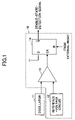
- FIG. 1 is a drawing showing an example of the configuration of an oscillating-signal-stable-state detecting circuit according to the present invention
- FIG. 2 is a drawing for explaining the circuit operation of the oscillating-signal-stable-state detecting circuit shown in FIG. 1 ;
- FIG. 3 is a drawing showing an example of the circuit configuration of a reference-voltage circuit.
- FIG. 4 is a drawing showing an example of the configuration of a semiconductor integrated circuit to which the present invention is applied.
- FIG. 1 is a drawing showing an example of the configuration of an oscillating-signal-stable-state detecting circuit according to the present invention.
- An oscillating-signal-stable-state detecting circuit 10 of FIG. 1 serves to determine whether the oscillating signal generated by an oscillator 11 has stabilized, and includes a reference-voltage circuit 12 , a comparator 13 , and a flip-flop 14 .
- the oscillator 11 may be a crystal oscillator, for example, and may be provided as a built-in component in the semiconductor integrated circuit to which the present invention is applied. If precision as high as that of a crystal oscillator is not required, a ceramic oscillator or the like may be used according to the application.
- the oscillating signal is not stable because the oscillation of the oscillator 11 has just begun. The amplitude of the oscillating signal is not sufficient during this waiting period before the stabilization of oscillation, and the oscillation waveform may easily be disturbed. If the oscillating signal in such a state is used as a clock signal in the semiconductor integrated circuit, the semiconductor integrated circuit may be running a risk of suffering malfunction.
- the oscillating-signal-stable-state detecting circuit 10 compares the amplitude of the oscillating signal generated by the oscillator 11 with a predetermined reference voltage, thereby determining whether the amplitude of the oscillating signal is sufficiently large in the stabilized state.
- the reference-voltage circuit 12 of the oscillating-signal-stable-state detecting circuit 10 serves to generate the reference voltage for comparison.
- the reference voltage generated by the reference-voltage circuit 12 is supplied to one input of the comparator 13 .
- the other input of the comparator 13 receives the oscillating signal generated by the oscillator 11 .
- the comparator 13 compares the oscillating signal generated by the oscillator 11 with the reference voltage generated by the reference-voltage circuit 12 , and sets its output to HIGH, for example, if the oscillating signal exceeds the reference voltage.
- the output of the comparator 13 is supplied to a clock input terminal CK of the flip-flop 14 .
- the flip-flop 14 is a D-flip-flop.
- the flip-flop 14 latches a signal supplied to its data input terminal D in response to a rising edge of the signal supplied to the clock input terminal CK.
- the data input terminal D is fixedly set to HIGH, so that the flip-flop 14 latches HIGH in response to a rise of the signal supplied from the comparator 13 to the clock input terminal CK.
- the flip-flop 14 is in the reset state (the state in which LOW is stored) owing to an external reset signal applied to its reset input R.
- This inverted output /Q (or non-inverted output Q (not shown)) serves as a stable-state detection signal indicative of the detection of a stable state of the oscillating signal.
- FIG. 2 is a drawing for explaining the circuit operation of the oscillating-signal-stable-state detecting circuit 10 shown in FIG. 1 .
- a letter designation (a) illustrates the oscillating signal output of the oscillator 11
- a letter designation (b) the comparison result output of the comparator 13
- a letter designation (c) the inverted output of the flip-flop 14 .
- a reference voltage VTH generated by the reference-voltage circuit 12 is also illustrated in addition to the oscillating signal output of the oscillator 11 .
- the oscillator output shown in (a) has a small amplitude, and has not yet reached a stable oscillation state. At this time, the oscillator output is lower than the reference voltage VTH at all times, so that the comparator output shown in (b) stays LOW. The flip-flop output shown in (c) is thus HIGH.
- the oscillator output shown in (a) gradually increases in amplitude.
- the comparator output shown in (b) becomes HIGH. Since the oscillator output being compared with the reference voltage VTH is oscillating, the comparator output shown in (b) alternates between HIGH and LOW like a clock signal after the amplitude of the oscillator output becomes sufficiently large.
- the flip-flop output shown in (c) changes from HIGH to LOW. Such LOW state of the flip-flop output indicates that the oscillating signal is in a sufficiently stable state.
- the reference-voltage circuit 12 is comprised of a potential divider that divides an external power supply voltage by use of resistance division, for example.
- a time length required for a voltage rise from zero voltage to the predetermined reference voltage VTH is thus far shorter than the time length required for the stabilization of the oscillator 11 . Accordingly, fluctuation of the voltage VTH of the reference-voltage circuit 12 at the time of power-on does not adversely affect the operation of the oscillating-signal-stable-state detecting circuit 10 .
- FIG. 3 is a drawing showing an example of the circuit configuration of the reference-voltage circuit 12 .
- the reference-voltage circuit 12 shown in FIG. 3 includes resistors 21 and 22 connected in series.
- the series of the resistors 21 and 22 connects between an external power supply voltage VDD and a ground voltage.
- the joint point between the resistor 21 and the resistor 22 generates the reference voltage VTH.
- the reference voltage VTH is supplied to one input of the comparator 13 as shown in FIG. 1 .
- FIG. 4 is a drawing showing an example of the configuration of the semiconductor integrated circuit to which the present invention is applied.
- the same elements as those of FIG. 1 are referred to by the same numerals, and a description thereof will be omitted.
- a semiconductor integrated circuit 100 shown in FIG. 4 includes the oscillating-signal-stable-state detecting circuit 10 , the oscillator 11 , a clock generating module 101 , a core circuit 102 , and an AND gate 103 .
- External terminals of the semiconductor integrated circuit 100 have a crystal resonator 105 coupled thereto.
- the oscillator 11 oscillates with predetermined frequency by utilizing a resonance effect of the crystal resonator 105 .
- the oscillating signal generated by the oscillator 11 is supplied to the oscillating-signal-stable-state detecting circuit 10 and the AND gate 103 .
- the oscillating-signal-stable-state detecting circuit 10 compares the amplitude of the oscillating signal from the oscillator 11 with a predetermined reference voltage, thereby determining whether the oscillating signal has stabilized after the power-on. When the oscillating signal stabilizes, the oscillating-signal-stable-state detecting circuit 10 sets its output signal to HIGH indicating the stable state of the oscillating signal. Namely, the non-inverted output Q, rather than the inverted output /Q, of the flip-flop 14 shown in FIG. 1 may be used as this output.
- the AND gate 103 blocks the oscillating signal supplied from the oscillator 11 .
- the AND gate 103 allows the oscillating signal from the oscillator 11 to pass, thereby supplying the oscillating signal to the clock generating module 101 .
- the clock generating module 101 generates various clock signals based on the stable oscillating signal supplied from the oscillator 11 through the AND gate 103 . These clock signals are supplied to the core circuit 102 .
- the core circuit 102 operates based on the clock signals supplied from the clock generating module 101 .
- the amplitude of the oscillating signal from the oscillator 11 is compared with the predetermined reference voltage, thereby determining whether the oscillating signal has become stable after the power on.
- a stable oscillating signal is supplied to the clock generating module 101 for generation of clock signals. This provides for stable circuit operations to be performed based on stable clock signals.
- FIG. 4 is merely an example of the semiconductor integrated circuit to which the present invention is applied, and a configuration for canceling the reset of the core circuit is not limited to such illustrated configuration.
- a reset input terminal may be provided for the core circuit, and a reset signal applied to this reset input terminal may be disabled in response to the stable-state-detection signal supplied from the oscillating-signal-stable-state detecting circuit 10 .
Landscapes
- Engineering & Computer Science (AREA)
- Theoretical Computer Science (AREA)
- Physics & Mathematics (AREA)
- General Engineering & Computer Science (AREA)
- General Physics & Mathematics (AREA)
- Nonlinear Science (AREA)
- Semiconductor Integrated Circuits (AREA)
- Oscillators With Electromechanical Resonators (AREA)
- Electronic Switches (AREA)
- Stabilization Of Oscillater, Synchronisation, Frequency Synthesizers (AREA)
Abstract
Description
Claims (6)
Applications Claiming Priority (2)
| Application Number | Priority Date | Filing Date | Title |
|---|---|---|---|
| JP2005-062660 | 2005-03-07 | ||
| JP2005062660A JP2006246367A (en) | 2005-03-07 | 2005-03-07 | Semiconductor integrated circuit and reset release method for semiconductor integrated circuit |
Publications (2)
| Publication Number | Publication Date |
|---|---|
| US20060197603A1 US20060197603A1 (en) | 2006-09-07 |
| US7310026B2 true US7310026B2 (en) | 2007-12-18 |
Family
ID=36943580
Family Applications (1)
| Application Number | Title | Priority Date | Filing Date |
|---|---|---|---|
| US11/272,068 Expired - Fee Related US7310026B2 (en) | 2005-03-07 | 2005-11-14 | Semiconductor integrated circuit with function to detect state of stable oscillation |
Country Status (2)
| Country | Link |
|---|---|
| US (1) | US7310026B2 (en) |
| JP (1) | JP2006246367A (en) |
Cited By (1)
| Publication number | Priority date | Publication date | Assignee | Title |
|---|---|---|---|---|
| US20090079510A1 (en) * | 2006-09-05 | 2009-03-26 | Meik Wilhelm Widmer | Integrated circuit and receiver of a global positioning system (gps) |
Families Citing this family (2)
| Publication number | Priority date | Publication date | Assignee | Title |
|---|---|---|---|---|
| JP5904167B2 (en) | 2013-07-17 | 2016-04-13 | 株式会社デンソー | Reset signal control device |
| KR101697527B1 (en) * | 2015-10-06 | 2017-01-19 | 울산과학기술원 | Protection circuit for preventing a digital circuitry from abnormal operations |
Citations (6)
| Publication number | Priority date | Publication date | Assignee | Title |
|---|---|---|---|---|
| US3553531A (en) * | 1968-05-09 | 1971-01-05 | Sits Soc It Telecom Siemens | Voltage stabilizer with overload protection and automatic restoration |
| US5369311A (en) * | 1992-03-06 | 1994-11-29 | Intel Corporation | Clock generator control circuit |
| US5673424A (en) * | 1993-08-06 | 1997-09-30 | Rohm Co., Ltd. | Circuit which supplies a clock pulse to a microcomputer |
| US6414559B1 (en) * | 1998-03-23 | 2002-07-02 | Dallas Semiconductor Corporation | Single package temperature compensated electronic device |
| JP2003216265A (en) | 2001-11-16 | 2003-07-31 | Matsushita Electric Ind Co Ltd | Oscillation stabilization detection circuit, oscillation form detection circuit using the same and integrated circuit device |
| US6798301B1 (en) * | 2001-06-11 | 2004-09-28 | Lsi Logic Corporation | Method and apparatus for controlling oscillation amplitude and oscillation frequency of crystal oscillator |
-
2005
- 2005-03-07 JP JP2005062660A patent/JP2006246367A/en active Pending
- 2005-11-14 US US11/272,068 patent/US7310026B2/en not_active Expired - Fee Related
Patent Citations (6)
| Publication number | Priority date | Publication date | Assignee | Title |
|---|---|---|---|---|
| US3553531A (en) * | 1968-05-09 | 1971-01-05 | Sits Soc It Telecom Siemens | Voltage stabilizer with overload protection and automatic restoration |
| US5369311A (en) * | 1992-03-06 | 1994-11-29 | Intel Corporation | Clock generator control circuit |
| US5673424A (en) * | 1993-08-06 | 1997-09-30 | Rohm Co., Ltd. | Circuit which supplies a clock pulse to a microcomputer |
| US6414559B1 (en) * | 1998-03-23 | 2002-07-02 | Dallas Semiconductor Corporation | Single package temperature compensated electronic device |
| US6798301B1 (en) * | 2001-06-11 | 2004-09-28 | Lsi Logic Corporation | Method and apparatus for controlling oscillation amplitude and oscillation frequency of crystal oscillator |
| JP2003216265A (en) | 2001-11-16 | 2003-07-31 | Matsushita Electric Ind Co Ltd | Oscillation stabilization detection circuit, oscillation form detection circuit using the same and integrated circuit device |
Cited By (1)
| Publication number | Priority date | Publication date | Assignee | Title |
|---|---|---|---|---|
| US20090079510A1 (en) * | 2006-09-05 | 2009-03-26 | Meik Wilhelm Widmer | Integrated circuit and receiver of a global positioning system (gps) |
Also Published As
| Publication number | Publication date |
|---|---|
| JP2006246367A (en) | 2006-09-14 |
| US20060197603A1 (en) | 2006-09-07 |
Similar Documents
| Publication | Publication Date | Title |
|---|---|---|
| US6695475B2 (en) | Temperature sensing circuit and method | |
| US8497741B2 (en) | High accuracy RC oscillator | |
| US8736314B2 (en) | Leakage power management using programmable power gating transistors and on-chip aging and temperature tracking circuit | |
| US8525603B2 (en) | Oscillating signal generating device and related method | |
| KR100668650B1 (en) | Clock Generation Circuit and Clock Generation Method | |
| KR20150054885A (en) | Low power clock source | |
| US6922084B2 (en) | Ultra-low power programmable timer and low voltage detection circuits | |
| CN107645288B (en) | Electronic circuit, method and electronic device for generating pulses | |
| US7310026B2 (en) | Semiconductor integrated circuit with function to detect state of stable oscillation | |
| US9007138B2 (en) | Oscillator with startup circuitry | |
| US9966900B2 (en) | Apparatus for oscillator with improved precision and associated methods | |
| US6900701B2 (en) | Automatic detection, selection and configuration of clock oscillator circuitry | |
| JP2017060120A (en) | Semiconductor device and oscillation circuit control method | |
| US6731708B1 (en) | Clock signal control device | |
| US6870353B2 (en) | Power supply control circuit and LSI using the same | |
| JP2921494B2 (en) | Oscillation circuit | |
| US6911873B2 (en) | Detection circuit and method for an oscillator | |
| US7642874B2 (en) | Oscillator circuit with transition detection enable | |
| US7642873B2 (en) | Method for enabling an oscillator circuit using transition detection | |
| JP4036114B2 (en) | Clock generation circuit | |
| US9362894B1 (en) | Clock generator circuit | |
| JPH01191064A (en) | Voltage detecting circuit | |
| KR101509421B1 (en) | Power-On-Reset Circuit Using Clock Signal and Peak Detector | |
| US11700003B2 (en) | Microcontroller, operation system and control method thereof | |
| JPH0778941A (en) | Overheat protection circuit in semiconductor integrated circuit |
Legal Events
| Date | Code | Title | Description |
|---|---|---|---|
| AS | Assignment |
Owner name: FUJITSU LIMITED, JAPAN Free format text: ASSIGNMENT OF ASSIGNORS INTEREST;ASSIGNOR:MIHO, AKIRA;REEL/FRAME:017235/0908 Effective date: 20051028 |
|
| FEPP | Fee payment procedure |
Free format text: PAYOR NUMBER ASSIGNED (ORIGINAL EVENT CODE: ASPN); ENTITY STATUS OF PATENT OWNER: LARGE ENTITY |
|
| AS | Assignment |
Owner name: FUJITSU MICROELECTRONICS LIMITED, JAPAN Free format text: ASSIGNMENT OF ASSIGNORS INTEREST;ASSIGNOR:FUJITSU LIMITED;REEL/FRAME:021998/0645 Effective date: 20081104 Owner name: FUJITSU MICROELECTRONICS LIMITED,JAPAN Free format text: ASSIGNMENT OF ASSIGNORS INTEREST;ASSIGNOR:FUJITSU LIMITED;REEL/FRAME:021998/0645 Effective date: 20081104 |
|
| REMI | Maintenance fee reminder mailed | ||
| LAPS | Lapse for failure to pay maintenance fees | ||
| STCH | Information on status: patent discontinuation |
Free format text: PATENT EXPIRED DUE TO NONPAYMENT OF MAINTENANCE FEES UNDER 37 CFR 1.362 |
|
| FP | Lapsed due to failure to pay maintenance fee |
Effective date: 20111218 |