US7280077B2 - System and method for measuring radiation characteristic of antenna - Google Patents
System and method for measuring radiation characteristic of antenna Download PDFInfo
- Publication number
- US7280077B2 US7280077B2 US10/540,333 US54033305A US7280077B2 US 7280077 B2 US7280077 B2 US 7280077B2 US 54033305 A US54033305 A US 54033305A US 7280077 B2 US7280077 B2 US 7280077B2
- Authority
- US
- United States
- Prior art keywords
- antenna
- tester
- measurement
- chip
- tester body
- Prior art date
- Legal status (The legal status is an assumption and is not a legal conclusion. Google has not performed a legal analysis and makes no representation as to the accuracy of the status listed.)
- Expired - Lifetime, expires
Links
Images


Classifications
-
- H—ELECTRICITY
- H01—ELECTRIC ELEMENTS
- H01Q—ANTENNAS, i.e. RADIO AERIALS
- H01Q1/00—Details of, or arrangements associated with, antennas
-
- G—PHYSICS
- G01—MEASURING; TESTING
- G01R—MEASURING ELECTRIC VARIABLES; MEASURING MAGNETIC VARIABLES
- G01R29/00—Arrangements for measuring or indicating electric quantities not covered by groups G01R19/00 - G01R27/00
- G01R29/08—Measuring electromagnetic field characteristics
- G01R29/10—Radiation diagrams of antennas
Definitions
- the present invention relates to a system and a method for measuring the radiation characteristic of an antenna, and more particularly, to an antenna measurement system and an antenna measurement method which speedily measure the radiation characteristic of a source antenna using micro-scaled test antennas and IC chips.
- the antenna ranges which are used to measure the radiation characteristic (the phase, or the intensity or amplitude) of the antenna are there a far-field range where the measurement is made while the source antenna is placed far from the tester or receiver antenna, a near-field range where the measurement is made by using the source antenna as a transmitter and taking samples near to source antenna with a probe per a predetermined distance, and a compact range where the measurement is made while the source antenna is placed near to a reflector antenna being the tester antenna.
- the far-field range is further classified into an elevated range where the measurement is made while the source antenna and the tester antenna are installed at a tower, a building or the top of a hill, a slant range where the measurement is made while one of the source and the tester antennas is placed at high position and the other on the ground, and an anechoic chamber where the measurement is made in a room having a wall with absorbents for removing the possible reflection.
- the elevated range and the slant range involve lower cost for the installation and measurement of the relevant elements, but practically require very wide area and high tower, with the disadvantage of being much influenced by the external weather.
- the anechoic chamber involves the indoor measurement, and is not influenced by the external weather, with the disadvantage in that much cost is needed to make a large laboratory (for example, making it with a vertical length of 10 m, a horizontal length of 10 m and a height of 5 m) with absorbents.
- the far-field distance r ff is determined to be 75 km. Accordingly, with the case of the elevated range or the slant range, the distance between the source and the tester antennas becomes enlarged. As various objects such as trees, forests, hills, rivers and buildings are existent between the source antenna and the tester antenna, it is very difficult to make the correct measurement, and to quickly cope with the variable measurement situations. Consequently, the measurement values are largely differentiated due to the difference in the temperature, and the weather. Moreover, with the case of the far-field range, the source antenna is exposed to the outside to obtain the correct measured values, and hence, it becomes difficult in the radar or military antennas to make the desired measurement while keeping a secret.
- the compact range is desirably installed within the relatively small space, but it undesirably requires a large-scaled reflector.
- the measurement may be made in a very small space provided that the inter-distance of minimally 1 wavelength is made to the source antenna.
- the probe should precisely move in the X and Y axial directions to correctly figure a predetermined plane (the plane perpendicular to the central axis of the source antenna) within the short distance, much time and cost are consumed to make the equipment for moving the probe (the tester antenna), and to make the desired measurement.
- the anechoic chamber also involves the same problem as with the near-field range in that the measurement is made using a probe.
- the correct data can be obtained only when the probe moves very precisely.
- the precision in the movement of the probe is several micrometers to several tens micrometers.
- As the carrier for moving the probe very precisely is made with a high cost of up to hundreds of millions, it is practically difficult with the small-scale companies to make measurement experiments related to the development of antennas in a sufficient manner.
- the carrier for moving the probe is liable to generate electromagnetic waves, which are applied to the measured values as noises.
- the antenna measurement system includes a tester body placed apart from the source antenna with a predetermined distance.
- a plurality of measurement modules are arranged at the tester body in a predetermined pattern.
- Each measurement module has an IC chip for processing positional information and measured values to generate relevant signals, and a tester antenna for receiving and transmitting the signals from the IC chip.
- the tester antenna Upon receipt of frequency signals from the source antenna, the tester antenna generates induced power for driving the IC chip, and transmits the measured values for the frequency signals to the IC chip.
- a measurement controller receives the signals from the tester antenna, and processes the positional information and the measured values of the respective measurement modules.
- a plurality of measurement modules are arranged at a tester body in a predetermined pattern.
- Each module has an IC chip for processing positional information and measured values to generate signals, and a tester antenna for receiving and transmitting the signals from the IC chip.
- the tester antenna Upon receipt of frequency signals from the source antenna, the tester antenna generates induced power for driving the IC chip, and transmits the measured values for the frequency signals to the IC chip.
- the tester body is placed apart from the source antenna with a predetermined distance such that the tester body is perpendicular to the central axis of the source antenna.
- the measurement controller With the operating of the source antenna, the measurement controller is operated such that it receives and data-processes the positional information and the measured values from the tester antenna of each measurement module provided at the tester body.
- a plurality of measurement modules are arranged at a tester body in a predetermined pattern.
- Each module has an IC chip for processing positional information and measured values to generate signals, and a tester antenna for receiving and transmitting the signals from the IC chip.
- the tester antenna Upon receipt of frequency signals from the source antenna, the tester antenna generates induced power for driving the IC chip, and transmits the measured values for the frequency signals to the IC chip.
- the source antenna is placed within the tester body such that it is positioned at the center of the tester body. With the operating of the source antenna, the measurement controller is operated such that it receives and data-processes the positional information and the measured values from the tester antenna of each measurement module provided at the tester body.
- the tester body is shaped with a plane, a circular arc, a sphere, a semi-sphere, a hexahedron, a hexahedron with no bottom side, a cone, a quadrangular pyramid, an octahedron, a dodecahedron, an icosahedron, or a horn.
- FIG. 1 is a schematic perspective view of an antenna measurement system according to a first embodiment of the present invention
- FIG. 2 is a plan view of a measurement module for the antenna measurement system shown in FIG. 1 ;
- FIG. 3 schematically illustrates a tester antenna for the antenna measurement system shown in FIG. 1 ;
- FIG. 4 schematically illustrates a first variation of the tester antenna shown in FIG. 3 ;
- FIG. 5 schematically illustrates a second variation of the tester antenna shown in FIG. 3 ;
- FIG. 6 schematically illustrates a third variation of the tester antenna shown in FIG. 3 ;
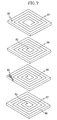
- FIG. 7 schematically illustrates a fourth variation of the tester antenna shown in FIG. 3 in an exploded manner
- FIG. 8 illustrates the bottom side of the tester antenna shown in FIG. 7 ;
- FIG. 9 is a graph illustrating the radiation pattern of the E-plane measured using the tester antenna shown in FIG. 4 ;
- FIG. 10 illustrates the state of the tester antenna measuring the x-y plane in the radiation pattern shown in FIG. 9 ;
- FIG. 11 illustrates the state of the tester antenna measuring the z-y plane in the radiation pattern shown in FIG. 9 ;
- FIG. 12 illustrates the state of the tester antenna measuring the z-x plane in the radiation pattern shown in FIG. 9 ;
- FIG. 13 is a block diagram illustrating the operation of the tester antenna and the IC chip
- FIG. 14 is a partial sectional perspective view of an antenna measurement system according to a second embodiment of the present invention.
- FIG. 15 is a partial sectional perspective view of an antenna measurement system according to a third embodiment of the present invention.
- FIG. 16 illustrates the antenna measurement system shown in FIG. 15 where the tester body is in a standing state
- FIG. 17 is a partial sectional perspective view of an antenna measurement system according to a fourth embodiment of the present invention.
- FIG. 18 is a partial sectional perspective view of an antenna measurement system according to a fifth embodiment of the present invention.
- FIG. 1 is a schematic perspective view of an antenna measurement system according to a first embodiment of the present invention
- FIG. 2 is a plan view of a measurement module for the antenna measurement system shown in FIG. 1 .
- the antenna measurement system includes a tester body 10 placed distant from a source antenna 2 by a predetermined distance, a plurality of measurement modules 20 arranged at the tester body 10 in a predetermined pattern, and a measurement controller 30 .
- Each measurement module 20 has an IC chip 22 for processing the positional information and the measured values to generate the relevant signals, and a tester antenna 24 for receiving and transmitting the signals from the IC chip 22 .
- the tester antenna 24 Upon receipt of the frequency signals from the source antenna 2 , the tester antenna 24 generates induced power for driving the IC chip 22 , and transmits the measured values for the frequency signals to the IC chip 22 .
- the measurement controller 30 receives the signals from the tester antennas 24 of the measurement modules 20 , and processes the positional information and the measured values of the respective measurement modules 20 .
- a receiver antenna 32 is installed at the measurement controller 30 to receive the signals from the tester antenna 24 .
- a built-in software makes transformation of the measured values into far-field range data.
- the tester body 10 is formed with a plane shape using a material little dispersed or reflected against the frequency signals from the source antenna 2 .
- the measurement module 20 has a substrate 21 shaped with a rectangle, a circle or an oval having a length or a maximum diameter of 2-4 mm.
- the IC chip 22 and the antenna 24 are mounted on the substrate 21 by a surface mounting technique.
- the IC chip 22 and/or the antenna 24 may be directly formed on the substrate 21 by printing or photolithography.
- the IC chip stores the number peculiar to its location. It is possible to use a coordination value as the characteristic number for the location stored at the IC chip 22 .
- the characteristic numbers are assigned thereto in the sequence of (X 1 , Y 1 ), (X 2 , Y 1 ), . . . , (Xm, Y 1 ).
- the characteristic numbers are assigned thereto in the sequence of (X 1 , Yn), (X 2 , Yn), . . . , (Xm, Yn).
- the IC chip 22 is programmed such that it transforms the values received at the tester antenna 24 related to the phase and the amplitude of the frequency signals or the dimension of the induced power into digital signals, and transmits them via the tester antenna 24 .
- the IC chip 22 As the IC chip 22 is currently made with several micrometers, it can be mounted on the substrate 21 with the micrometer-leveled size.
- An amplification circuit is preferably installed at the IC chip 22 to amplify the micro-scaled frequency signal or induced power, and obtain precise measurement results.
- the IC chip 22 is programmed such that it combines the measured value from the tester antenna 24 with the characteristic numbers in a predetermined sequence to generate a predetermined measurement signal, and transmits it via the tester antenna 24 together with the trigger signal.
- the tester antenna 24 has a micro-scaled size such that it can be mounted on the substrate 21 with a very small size.
- a microstrip patch antenna or a dielectric chip antenna can be used as the micro tester antenna with a size of several millimeters.
- the tester antenna 24 may have an ultra-micro size such that it can be mounted on the substrate 21 with a micrometer size.
- the measurement module 20 becomes enlarged. In this case, it is impossible to make the measurement per a minute distance, and accordingly, a correct measurement value cannot be obtained with the transformation of the measured values into far-field range data. Furthermore, in case the tester antenna 24 has a large size, it is likely that an error may be made in the measured values due to the impedance variation by the inter-coupling of the neighboring antennas. Therefore, in order to obtain the correct measured values, it is necessary to minimize the tester antenna 24 .
- the tester antenna 24 has wires spirally wound on two or more-leveled imagined planes, respectively.
- the wires formed at the imagined plane neighbors are connected to each other at their central ends or peripheral ends to form a single line.
- the antenna 24 has wires 42 , 44 and 46 spirally wound on first to third imagined planes.
- the wires 42 and 44 formed at the first and second imagined planes are connected to each other at their central ends using an interconnection line 43 .
- the wires 44 and 46 formed at the second and third imagined planes are connected to each other at their peripheral ends using an interconnection line 45 .
- a feeder 48 is connected to the peripheral end of the wire 42 formed at the bottommost first imagined plane.
- wires 42 , 44 and 46 and the interconnection lines 43 and 45 are elongated by holding the peripheral end of the wire 46 and the feeder 48 , the whole wire portions make formation of a single line.
- the wires 42 , 44 and 46 may be outlined with various shapes, such as a rectangle, a circle, an oval, a hexagon, or an octagon.
- the distance between the neighboring wires 42 , 44 and 45 is narrowed so that the inter-impedance thereof is maximized to thereby compensate for the increased capacitance.
- an insulating layer (not shown) between the wires 42 , 44 and 46 to prevent the possible short-circuiting.
- the tester antenna 24 may have wires 52 and 54 spirally wound on the two-leveled imagined planes, respectively.
- the wires 52 and 54 are connected to each other at their peripheral ends using an interconnection line 55 .
- a feeder 58 is connected to the central end of the wire 52 formed at the lower imagined plane.
- FIG. 9 illustrates the radiation pattern of the E-plane measured at 390 MHz while the tester antennas 24 are arranged in various directions as illustrated in FIGS. 10 to 12 .
- the radiation pattern is measured by establishing the distance between the transmitter side of the tester antenna and the receiver side thereof to be 122 cm, and the heights thereof identically to be 204 cm.
- the tester antenna 24 is structured such that the horizontal length of the outermost spiral portion thereof is established to be ⁇ /86.2 mm of the wavelength ( ⁇ ), and the vertical length thereof to be ⁇ /57.1 mm.
- the antenna portions are wound four times with the same distance, and the height of the two imagined planes is established to be ⁇ /285.7 mm.
- the x-y plane of FIG. 9 was measured by installing the tester antenna 24 to be in the state illustrated in FIG. 10 .
- the z-y plane was measured by installing the tester antenna 24 to be in the state illustrated in FIG. 11 .
- the z-x plane was measured by installing the tester antenna 24 in the state illustrated in FIG. 12 .
- the three cases all exhibited a radiation pattern similar to that of the dipole antenna.
- the tester antenna 24 may have five wires 62 , 64 , 66 , 67 and 69 spirally wound on the five-leveled imagined planes.
- the wires 62 and 64 formed at the first and second imagined plane neighbors as well as the wires 66 and 67 formed at the third and fourth imagined plane neighbors are connected to each other at their peripheral ends using interconnection lines 63 .
- the wires 64 and 66 formed at the second and third imagined plane neighbors as well as the wires 67 and 69 formed at the fourth and fifth imagined plane neighbors are connected to each other at their central ends using interconnection lines 65 .
- a feeder 68 is connected to the central end of the wire 62 formed at the bottommost imagined plane.
- the tester antenna 24 is structured such that the wires formed at the imagined plane neighbors are connected to each other repeatedly at their central ends and at their peripheral ends in an alternate manner while wholly forming a single line.
- the tester antenna 24 may be structured such that the wires 72 , 74 and 76 formed at the imagined planes are spirally wound each in the shape of an oval, and connected to each other using interconnection lines 73 and 75 while forming a single line.
- a feeder 78 is connected to the bottommost wire 72 .
- the antenna 24 may be structured such that four dielectric films 80 are placed at first to fourth imagined planes, and spiral wires 82 , 84 , 86 and 87 are printed on the one-sided surfaces thereof.
- Through holes 83 are formed at the first and third-leveled dielectric thin films 80 such that they are connected to the central ends of the wires 82 and 86 .
- Through holes 85 are formed at the second and fourth-leveled dielectric thin films such that they are connected to the peripheral ends of the wires 84 and 87 .
- the through holes 83 and 85 are filled with conductive powder, and the four dielectric thin films are closely adhered to each other to form a single chip. The chip is heated at a predetermined temperature, and the conductive powder in the through holes 83 and 85 are molten so that the wire neighbors are connected to each other to form a single line.
- the dielectric thin film where the through hole is connected to the central end of the wire, and the dielectric thin film where the through hole is connected to the peripheral end of the wire are alternately deposited.
- a feeder 88 is formed at the bottom side of the bottommost dielectric thin film 80 such that it is connected to the through hole 83 .
- the spiral wires 82 , 84 , 86 and 87 and the feeder 88 are formed at the dielectric thin films 80 by a printing technique or a photolithography technique commonly used in the semiconductor manufacturing process.
- the tester antenna 24 is formed with the above structure, it is possible to make the tester antenna with a micrometer-scaled size such that it can be mounted on the substrate 21 having a size of several micrometers together with the IC chip 22 .
- a receiver antenna 32 is installed at the measurement controller 30 to receive the signals from the tester antenna 24 .
- the measurement controller 30 transforms the signals received at the receiver antenna 32 , and displays them by a monitor, or outputs them by a printer. It stores the positional information of the measurement modules 20 as well as the measured values.
- the values measured at the tester antenna 24 and transmitted to the measurement controller 30 are the phase and the amplitude of the frequency signals from the source antenna 2 .
- measurement modules 20 each with an IC chip 22 storing the positional information intrinsic thereto and a tester antenna 24 are mounted at the predetermined locations of a tester body 10 .
- the tester body 10 When the tester body 10 is made, it is placed at the predetermined location (distant from the source antenna by 1 wavelength of the frequency therefrom), and the source antenna 2 is operated.
- the tester antenna 24 of the measurement module 20 installed at the tester body 10 receives the frequency signals (the electromagnetic waves) from the source antenna 2 , which partially generate induced power (using an RF-DC rectifier) to drive the IC chip 22 .
- the IC chip 22 uses the induced power from the tester antenna 24 without requiring a separate power supply. Therefore, when a large-sized tester body 10 is made, or even when a large number of measurement modules 20 are mounted on the tester body 10 , the wire for the power supplying is unneeded, and the structure is simplified while ensuring the easy making thereof.
- the IC chip 22 of the measurement module 20 samples the amplitude and the phase of the frequency and the dimension of the induced power from the tester antenna 24 , and stores and modulates them (using PSK and/or FSK modulation or CDMA).
- the IC chip 22 transmits the positional information and the modulated signals via the tester antenna 24 .
- the measurement controller 30 receives the signals from the tester antenna 24 via the receiver antenna 32 , and data-processes the positional information and the modulated signals of the respective measurement modules 20 to compute and store the data.
- the data are output by a display device or a printer.
- the measurement controller 30 has a built-in software to transform the measured values from the measurement modules 20 into the data of the far-field range, and output them by a display device or a printer.
- the measurement is made once more while the source antenna 2 is rotated by 180°, or the installation position of the tester body 10 is varied by 180° to that position symmetrical thereto. Even in this case, as the measurement time is extremely short, the time consumption is reduced significantly compared to the conventional case.
- FIG. 14 illustrates an antenna measurement system according to a second embodiment of the present invention.
- the tester body 12 is shaped with a sphere, and the measurement modules 20 are arranged on the inner surface of the tester body 12 in a predetermined pattern.
- the tester body 12 is formed with a spherical shape, it is bisected into upper and lower parts. With this structure, it is easy to install and replace the source antenna 2 within the tester body 12 .
- the source antenna 2 is fixed to a support 3 placed at the lower part of the tester body 12 such that it is positioned at the center of the spherical shaped structure. It is preferable to structure the source antenna 2 such that the height thereof can be varied in a controlled manner.
- the tester body 12 When the tester body 12 is formed with a spherical shape, it is possible to correctly measure the all directional (360°) characteristic of the source antenna 2 only with the one-timed measurement.
- the measurement module 20 installed at the tester body 12 is structured that the tester antenna 24 is positioned perpendicular to the radius (r) of the tester body 12 being the measurement distance, thereby being located vertical to the progressive direction of the electromagnetic wave.
- the tester body 12 is preferably structured such that the radius (r) thereof being the distance from the source antenna 2 to the measurement module 20 becomes enlarged as much as possible.
- FIG. 15 illustrates an antenna measurement system according to a third embodiment of the present invention.
- the tester body 14 is formed with a semi-spherical shape, and the measurement modules 20 are arranged internal to the tester body 14 in a predetermined pattern.
- the characteristic positional number of each measurement module 20 is input into the IC chip 22 using the coordination value ( ⁇ , ⁇ ) with the angle ( ⁇ ) to the z axis and the angle ( ⁇ ) to the x axis.
- the structure of the tester body 14 according to the third embodiment of the present invention is the same as the upper part of the tester body 12 according to the second embodiment.
- the structure according to the third embodiment is more effective than that according to the second embodiment.
- the tester body 14 is formed with a semi-spherical shape, as shown in FIG. 16 , it is possible that the tester body 14 is in a standing state as like with the structure related to the first embodiment, and the measurement is made while the source antenna 2 is placed on the extended line of the center of the tester body 14 .
- the plane-shaped tester body 10 according to the first embodiment is replaced by the semi-spherical shaped tester body 14 according to the third embodiment.
- FIG. 17 illustrates an antenna measurement system according to a fourth embodiment of the present invention.
- the tester body is shaped with a hexahedron, and the measurement modules 20 are arranged at the inner surface of the tester body 16 in a predetermined pattern.
- the characteristic positional number of each measurement module 20 is input into the IC chip 22 using the three dimensional coordination values (x, y, z).
- the manufacturing and the installation thereof can be easily made compared to the case where it is formed with the spherical shape.
- the hexahedron-shaped tester body 16 is formed with a combinatory structure where it is bisected into upper and lower parts, which are combined with each other.
- FIG. 18 illustrates an antenna measurement system according to a fifth embodiment of the present invention.
- the tester body 18 is shaped with a hexahedron where the bottom side is removed, and the measurement modules 20 are arranged internal to the tester body 18 in a predetermined pattern.
- the structure of the tester body 18 according to the fifth embodiment is the same as the upper part of the tester body 16 according to the fourth embodiment.
- the structure according to the fifth embodiment is more effective than that according to the fourth embodiment.
- Measurement modules 20 each with an IC chip 22 storing the characteristic positional information and a tester antenna 24 are arranged at a tester body 10 in a predetermined pattern.
- the source antenna 2 is operated while it is placed at the predetermined center location within the tester body 10 .
- the tester antenna 24 of the measurement module 20 internally placed on the tester body 10 receives the frequency signals (the electromagnetic waves) from the source antenna 2 .
- the frequency signals the electromagnetic waves
- the antenna characteristic of the source antenna 2 is measured in the above way, the all-directional characteristic thereof can be correctly known with the one-timed measurement. Furthermore, the measurement is effectively made within the indoor space, and the total inspection can be made at the antenna production site.
- the tester body 12 , 14 , 16 or 8 is shaped with a sphere, a semi-sphere, a hexahedron, or a hexahedron with no bottom side. Alternatively, it may be shaped with an octahedron, a dodecahedron, an icosahedron, a cone, a quadrangular pyramid, or a horn.
- the tester body 10 is shaped with a plane. Alternatively, it may be shaped with a circular arc, a semicircle, a cone, a quadrangular pyramid, or a horn.
- the source antenna is operated, and at the same time, the entire area of the tester body is measured. This makes it possible to conduct the desired measurement in real time.
- the inventive system and method for measuring the radiation characteristic of an antenna it is possible to make a very small-scaled tester antenna. Furthermore, it is also possible to precisely install measurement modules at the tester body per a very small distance (2-3 ⁇ m). Consequently, the characteristic of the source antenna (the phase, and the intensity or amplitude of the frequency signal) can be simply and correctly measured in real time. The measurement is made without making any error due to the variation in the weather or the temperature.
- the total facility cost is significantly reduced. Accordingly, it is possible to conduct measuring and testing the antenna radiation characteristic in small-scaled factories or institutes.
- the inventive system and method for measuring the radiation characteristic of an antenna with some installation space for the plane-shaped or spherical-shaped tester body, it is possible to measure the characteristic of the source antenna. Therefore, it is possible to make larger the volume of the tester body or to make the arrangement distance between the measurement modules very small. In this way, it is possible to obtain more precise far-field range data.
- the inventive system and method for measuring the radiation characteristic of an antenna as it is possible to make the tester antenna in a very small scale, the impedance variation due to the inter-coupling of the neighboring antennas is extremely small even when the distance between the measurement modules is established to be several micrometers. Accordingly, even in such as case, the desired precise measurement values can be well obtained.
Landscapes
- Physics & Mathematics (AREA)
- Electromagnetism (AREA)
- General Physics & Mathematics (AREA)
- Variable-Direction Aerials And Aerial Arrays (AREA)
Abstract
Description
Claims (12)
Applications Claiming Priority (3)
| Application Number | Priority Date | Filing Date | Title |
|---|---|---|---|
| KR20020081538 | 2002-12-20 | ||
| KR1020020081538 | 2002-12-20 | ||
| PCT/KR2003/002788 WO2004057349A1 (en) | 2002-12-20 | 2003-12-19 | System and method for measuring radiation characteristic of antenna |
Publications (2)
| Publication Number | Publication Date |
|---|---|
| US20060057985A1 US20060057985A1 (en) | 2006-03-16 |
| US7280077B2 true US7280077B2 (en) | 2007-10-09 |
Family
ID=32677739
Family Applications (1)
| Application Number | Title | Priority Date | Filing Date |
|---|---|---|---|
| US10/540,333 Expired - Lifetime US7280077B2 (en) | 2002-12-20 | 2003-12-19 | System and method for measuring radiation characteristic of antenna |
Country Status (4)
| Country | Link |
|---|---|
| US (1) | US7280077B2 (en) |
| KR (1) | KR100543725B1 (en) |
| AU (1) | AU2003286971A1 (en) |
| WO (1) | WO2004057349A1 (en) |
Cited By (8)
| Publication number | Priority date | Publication date | Assignee | Title |
|---|---|---|---|---|
| US20060267138A1 (en) * | 2005-05-30 | 2006-11-30 | Semiconductor Energy Laboratory Co., Ltd. | Semiconductor device |
| US20070090999A1 (en) * | 2005-10-24 | 2007-04-26 | Samsung Electronics Co., Ltd. | Self-biased receiver system using a multi-fed antenna |
| US20110134000A1 (en) * | 2009-12-07 | 2011-06-09 | Electronics And Telecommunications Research Institute | Apparatus and method for detecting radiated power |
| US20110193566A1 (en) * | 2006-04-05 | 2011-08-11 | Emscan Corporation | Multichannel absorberless near field measurement system |
| US20130207680A1 (en) * | 2010-10-08 | 2013-08-15 | Satimo Industries | Device for the electromagnetic testing of an object |
| US20150116164A1 (en) * | 2013-10-29 | 2015-04-30 | Mi Technologies, Llc | Radiation measurement system and method with synchronous high speed tracking laser based position measurement |
| US20150253452A1 (en) * | 2014-03-07 | 2015-09-10 | avaSensor, LLC | Matter detector, sensor and locator device and methods of operation |
| US11927614B2 (en) | 2018-07-06 | 2024-03-12 | Samsung Electronics Co., Ltd | Chamber for measuring performance of antenna and system including same |
Families Citing this family (15)
| Publication number | Priority date | Publication date | Assignee | Title |
|---|---|---|---|---|
| KR100802181B1 (en) * | 2006-04-10 | 2008-02-12 | 한국전자통신연구원 | Antenna Radiation Pattern Measurement System and Method in Fresnel Region |
| EP1870718A1 (en) | 2006-06-23 | 2007-12-26 | The Swatch Group Research and Development Ltd. | System for measuring the radiation diagram of a transmission antenna |
| KR100776679B1 (en) * | 2006-09-27 | 2007-11-16 | 한국전자통신연구원 | Method of measuring antenna characteristics in non-operating frequency band of chamber |
| KR100826527B1 (en) * | 2006-12-04 | 2008-04-30 | 한국전자통신연구원 | Antenna Radiation Pattern Measurement System and Method in Fresnel Region Using Pie Change Method |
| KR100796625B1 (en) * | 2007-01-04 | 2008-01-22 | (주)케이티엠테크놀로지 | Hemispherical Antenna Chamber |
| KR20100079644A (en) | 2008-12-31 | 2010-07-08 | 충남대학교산학협력단 | Measuring method of radiation characteristic for antenna |
| DE102009018925A1 (en) * | 2009-04-28 | 2010-11-04 | Astrium Gmbh | Method and arrangement for measuring the directional characteristic of an antenna to be tested |
| US9002287B2 (en) * | 2009-10-09 | 2015-04-07 | Apple Inc. | System for testing multi-antenna devices |
| KR101012161B1 (en) * | 2010-08-25 | 2011-02-07 | 엘아이지넥스원 주식회사 | System and method for measuring antenna pattern of digital radar |
| KR101255478B1 (en) | 2011-07-27 | 2013-04-16 | 선문대학교 산학협력단 | the test system to measure wireless sign |
| US9255953B2 (en) * | 2012-02-16 | 2016-02-09 | Src, Inc. | System and method for antenna pattern estimation |
| US9116232B2 (en) | 2012-04-13 | 2015-08-25 | Apple Inc. | Methods and apparatus for testing satellite navigation system receiver performance |
| CN112230071B (en) * | 2019-07-15 | 2024-04-12 | 川升股份有限公司 | Antenna radiation measurement system to improve RF signal stability |
| NL2026930B1 (en) * | 2020-11-19 | 2022-07-01 | Univ Delft Tech | 3D Real-Time Antenna Characterization |
| KR102839881B1 (en) * | 2021-11-19 | 2025-07-31 | 대한민국 | System for measuring performance of EUT and method thereof |
Citations (8)
| Publication number | Priority date | Publication date | Assignee | Title |
|---|---|---|---|---|
| US4531126A (en) | 1981-05-18 | 1985-07-23 | Societe D'etude Du Radant | Method and device for analyzing a very high frequency radiation beam of electromagnetic waves |
| US5128621A (en) | 1987-04-21 | 1992-07-07 | Centre National De La Recherche Scientifique | Device for measuring, at a plurality of points, the microwave field diffracted by an object |
| US5430369A (en) | 1990-06-14 | 1995-07-04 | Societe D'applications Technologiques De L'imagerie | Device for measuring, at a plurality of points of a surface, the microwave field radiated by a source |
| US5477229A (en) | 1992-10-01 | 1995-12-19 | Alcatel Espace | Active antenna near field calibration method |
| US6236362B1 (en) * | 1999-04-20 | 2001-05-22 | Harris Corporation | Mitigation of antenna test range impairments caused by presence of undesirable emitters |
| US20030173990A1 (en) | 2000-11-13 | 2003-09-18 | Mitsue Nanbu | Wafer map display apparatus and method for semiconductor test system |
| US7035594B2 (en) * | 2001-07-02 | 2006-04-25 | Qualcomm Inc. | Method and apparatus for testing and evaluating wireless communication devices |
| US7170457B2 (en) * | 2004-05-12 | 2007-01-30 | Miao-Yu Chien | Mobile electromagnetic compatibility (EMC) test laboratory |
-
2003
- 2003-12-19 US US10/540,333 patent/US7280077B2/en not_active Expired - Lifetime
- 2003-12-19 AU AU2003286971A patent/AU2003286971A1/en not_active Abandoned
- 2003-12-19 WO PCT/KR2003/002788 patent/WO2004057349A1/en not_active Application Discontinuation
- 2003-12-19 KR KR1020030093537A patent/KR100543725B1/en not_active Expired - Lifetime
Patent Citations (8)
| Publication number | Priority date | Publication date | Assignee | Title |
|---|---|---|---|---|
| US4531126A (en) | 1981-05-18 | 1985-07-23 | Societe D'etude Du Radant | Method and device for analyzing a very high frequency radiation beam of electromagnetic waves |
| US5128621A (en) | 1987-04-21 | 1992-07-07 | Centre National De La Recherche Scientifique | Device for measuring, at a plurality of points, the microwave field diffracted by an object |
| US5430369A (en) | 1990-06-14 | 1995-07-04 | Societe D'applications Technologiques De L'imagerie | Device for measuring, at a plurality of points of a surface, the microwave field radiated by a source |
| US5477229A (en) | 1992-10-01 | 1995-12-19 | Alcatel Espace | Active antenna near field calibration method |
| US6236362B1 (en) * | 1999-04-20 | 2001-05-22 | Harris Corporation | Mitigation of antenna test range impairments caused by presence of undesirable emitters |
| US20030173990A1 (en) | 2000-11-13 | 2003-09-18 | Mitsue Nanbu | Wafer map display apparatus and method for semiconductor test system |
| US7035594B2 (en) * | 2001-07-02 | 2006-04-25 | Qualcomm Inc. | Method and apparatus for testing and evaluating wireless communication devices |
| US7170457B2 (en) * | 2004-05-12 | 2007-01-30 | Miao-Yu Chien | Mobile electromagnetic compatibility (EMC) test laboratory |
Non-Patent Citations (1)
| Title |
|---|
| International Search Report; International Application No. PCT/KR 03/02788-0; Date of Report: Feb. 23, 2004 by Austrian Patent Office, Dresdner Strabetae, Vienna. |
Cited By (14)
| Publication number | Priority date | Publication date | Assignee | Title |
|---|---|---|---|---|
| US20060267138A1 (en) * | 2005-05-30 | 2006-11-30 | Semiconductor Energy Laboratory Co., Ltd. | Semiconductor device |
| US7688272B2 (en) * | 2005-05-30 | 2010-03-30 | Semiconductor Energy Laboratory Co., Ltd. | Semiconductor device |
| US20070090999A1 (en) * | 2005-10-24 | 2007-04-26 | Samsung Electronics Co., Ltd. | Self-biased receiver system using a multi-fed antenna |
| US7853223B2 (en) * | 2005-10-24 | 2010-12-14 | Samsung Electronics Co., Ltd. | Self-biased receiver system using a multi-fed antenna |
| US8502546B2 (en) | 2006-04-05 | 2013-08-06 | Emscan Corporation | Multichannel absorberless near field measurement system |
| US20110193566A1 (en) * | 2006-04-05 | 2011-08-11 | Emscan Corporation | Multichannel absorberless near field measurement system |
| US20110134000A1 (en) * | 2009-12-07 | 2011-06-09 | Electronics And Telecommunications Research Institute | Apparatus and method for detecting radiated power |
| US8547284B2 (en) * | 2009-12-07 | 2013-10-01 | Electronics And Telecommunications Research Institute | Apparatus and method for detecting radiated power |
| US20130207680A1 (en) * | 2010-10-08 | 2013-08-15 | Satimo Industries | Device for the electromagnetic testing of an object |
| US9267967B2 (en) * | 2010-10-08 | 2016-02-23 | Satimo Industries | Device for the electromagnetic testing of an object |
| US20150116164A1 (en) * | 2013-10-29 | 2015-04-30 | Mi Technologies, Llc | Radiation measurement system and method with synchronous high speed tracking laser based position measurement |
| US9726704B2 (en) * | 2013-10-29 | 2017-08-08 | Nsi-Mi Technologies, Llc | Radiation measurement system and method with synchronous high speed tracking laser based position measurement |
| US20150253452A1 (en) * | 2014-03-07 | 2015-09-10 | avaSensor, LLC | Matter detector, sensor and locator device and methods of operation |
| US11927614B2 (en) | 2018-07-06 | 2024-03-12 | Samsung Electronics Co., Ltd | Chamber for measuring performance of antenna and system including same |
Also Published As
| Publication number | Publication date |
|---|---|
| AU2003286971A8 (en) | 2004-07-14 |
| KR100543725B1 (en) | 2006-01-20 |
| KR20040055671A (en) | 2004-06-26 |
| AU2003286971A1 (en) | 2004-07-14 |
| WO2004057349A1 (en) | 2004-07-08 |
| US20060057985A1 (en) | 2006-03-16 |
Similar Documents
| Publication | Publication Date | Title |
|---|---|---|
| US7280077B2 (en) | System and method for measuring radiation characteristic of antenna | |
| JP7213035B2 (en) | Test equipment, test systems and test methods | |
| CN113661397B (en) | Test arrangement, automated test equipment, and method for testing a device under test comprising a circuit and an antenna coupled to the circuit | |
| CN112204406A (en) | Wireless test fixture using antenna array, method for performing wireless production test | |
| US20100066619A1 (en) | Magnetic coupling device and reading device | |
| US8729909B2 (en) | Radio wave intensity measuring device and radio wave measuring system | |
| TW201939047A (en) | Localized free space tester | |
| CN209841969U (en) | Compact range antenna test system | |
| KR20220052912A (en) | Test apparatus, automated test equipment and method for testing DUT including antenna | |
| CN113419116A (en) | Passive performance test system and test method suitable for whole vehicle-level antenna | |
| JP2000338155A (en) | Antenna measurement system | |
| Toivanen et al. | Rfid-based book finder [education corner] | |
| Jabbar et al. | AWideband frequency Beam-Scanning antenna array for Millimeter-Wave industrial wireless sensing applications | |
| US8284108B2 (en) | Method of measuring radiation characteristic of antenna | |
| EP1570257B1 (en) | System for measuring the specific absorption rate (sar) comprising a plurality of microantennas and associated ic chips in a phantom | |
| CN115753837A (en) | Plane wave generator and plane wave generator testing system | |
| CN115754491B (en) | Plane wave generator and plane wave generator test system | |
| TWM639827U (en) | Separate Test Equipment | |
| JP7702680B1 (en) | Inspection Probe Head | |
| JP4673214B2 (en) | RFID tag test method and test system | |
| Qing et al. | Antenna Measurement Setups: Introduction | |
| Mai-Khanh et al. | A Low-Cost Planar Arrow-Shaped Monopole Antenna for 5G Near-Field Measurement | |
| CN117783698A (en) | VHF antenna double-unmanned aerial vehicle testing system and method | |
| Cudrnak | RFID Modeling, Characterization, and Optimization |
Legal Events
| Date | Code | Title | Description |
|---|---|---|---|
| AS | Assignment |
Owner name: THE INDUSTRY & ACADEMIC COOPERATION IN CHUNGNAM NA Free format text: ASSIGNMENT OF ASSIGNORS INTEREST;ASSIGNOR:THE EDUCATION & RESEARCH FOUNDATION FOR INDUSTRY, UNIVERSITY AND RESEARCH INSTITUTE IN CHUNGNAM NATIONAL UNIVERSITY;REEL/FRAME:019601/0384 Effective date: 20050902 Owner name: VIGITASYSTEM INC., JAPAN Free format text: ASSIGNMENT OF ASSIGNORS INTEREST;ASSIGNOR:THE EDUCATION & RESEARCH FOUNDATION FOR INDUSTRY, UNIVERSITY AND RESEARCH INSTITUTE IN CHUNGNAM NATIONAL UNIVERSITY;REEL/FRAME:019601/0384 Effective date: 20050902 Owner name: AMPLET INC., JAPAN Free format text: ASSIGNMENT OF ASSIGNORS INTEREST;ASSIGNOR:THE EDUCATION & RESEARCH FOUNDATION FOR INDUSTRY, UNIVERSITY AND RESEARCH INSTITUTE IN CHUNGNAM NATIONAL UNIVERSITY;REEL/FRAME:019601/0384 Effective date: 20050902 Owner name: THE EDUCATION & RESEARCH FOUNDATION FOR INDUSTRY, Free format text: ASSIGNMENT OF ASSIGNORS INTEREST;ASSIGNORS:WOO, JONG-MYUNG;KIM, JONG-LAE;REEL/FRAME:019601/0356 Effective date: 20050902 Owner name: AMPLET INC., JAPAN Free format text: ASSIGNMENT OF ASSIGNORS INTEREST;ASSIGNORS:WOO, JONG-MYUNG;KIM, JONG-LAE;REEL/FRAME:019601/0356 Effective date: 20050902 Owner name: VIGITASYSTEM INC., JAPAN Free format text: ASSIGNMENT OF ASSIGNORS INTEREST;ASSIGNORS:WOO, JONG-MYUNG;KIM, JONG-LAE;REEL/FRAME:019601/0356 Effective date: 20050902 |
|
| STCF | Information on status: patent grant |
Free format text: PATENTED CASE |
|
| FEPP | Fee payment procedure |
Free format text: PAYOR NUMBER ASSIGNED (ORIGINAL EVENT CODE: ASPN); ENTITY STATUS OF PATENT OWNER: SMALL ENTITY |
|
| FPAY | Fee payment |
Year of fee payment: 4 |
|
| FPAY | Fee payment |
Year of fee payment: 8 |
|
| MAFP | Maintenance fee payment |
Free format text: PAYMENT OF MAINTENANCE FEE, 12TH YR, SMALL ENTITY (ORIGINAL EVENT CODE: M2553); ENTITY STATUS OF PATENT OWNER: SMALL ENTITY Year of fee payment: 12 |