US7273794B2 - Shallow trench isolation fill by liquid phase deposition of SiO2 - Google Patents
Shallow trench isolation fill by liquid phase deposition of SiO2 Download PDFInfo
- Publication number
- US7273794B2 US7273794B2 US10/732,953 US73295303A US7273794B2 US 7273794 B2 US7273794 B2 US 7273794B2 US 73295303 A US73295303 A US 73295303A US 7273794 B2 US7273794 B2 US 7273794B2
- Authority
- US
- United States
- Prior art keywords
- silicon dioxide
- shallow trench
- trench isolation
- isolation region
- layer
- Prior art date
- Legal status (The legal status is an assumption and is not a legal conclusion. Google has not performed a legal analysis and makes no representation as to the accuracy of the status listed.)
- Expired - Fee Related, expires
Links
Images


Classifications
-
- H—ELECTRICITY
- H10—SEMICONDUCTOR DEVICES; ELECTRIC SOLID-STATE DEVICES NOT OTHERWISE PROVIDED FOR
- H10D—INORGANIC ELECTRIC SEMICONDUCTOR DEVICES
- H10D86/00—Integrated devices formed in or on insulating or conducting substrates, e.g. formed in silicon-on-insulator [SOI] substrates or on stainless steel or glass substrates
- H10D86/201—Integrated devices formed in or on insulating or conducting substrates, e.g. formed in silicon-on-insulator [SOI] substrates or on stainless steel or glass substrates the substrates comprising an insulating layer on a semiconductor body, e.g. SOI
-
- H—ELECTRICITY
- H10—SEMICONDUCTOR DEVICES; ELECTRIC SOLID-STATE DEVICES NOT OTHERWISE PROVIDED FOR
- H10D—INORGANIC ELECTRIC SEMICONDUCTOR DEVICES
- H10D86/00—Integrated devices formed in or on insulating or conducting substrates, e.g. formed in silicon-on-insulator [SOI] substrates or on stainless steel or glass substrates
- H10D86/01—Manufacture or treatment
-
- H—ELECTRICITY
- H10—SEMICONDUCTOR DEVICES; ELECTRIC SOLID-STATE DEVICES NOT OTHERWISE PROVIDED FOR
- H10P—GENERIC PROCESSES OR APPARATUS FOR THE MANUFACTURE OR TREATMENT OF DEVICES COVERED BY CLASS H10
- H10P90/00—Preparation of wafers not covered by a single main group of this subclass, e.g. wafer reinforcement
- H10P90/19—Preparing inhomogeneous wafers
- H10P90/1904—Preparing vertically inhomogeneous wafers
- H10P90/1906—Preparing SOI wafers
-
- H—ELECTRICITY
- H10—SEMICONDUCTOR DEVICES; ELECTRIC SOLID-STATE DEVICES NOT OTHERWISE PROVIDED FOR
- H10W—GENERIC PACKAGES, INTERCONNECTIONS, CONNECTORS OR OTHER CONSTRUCTIONAL DETAILS OF DEVICES COVERED BY CLASS H10
- H10W10/00—Isolation regions in semiconductor bodies between components of integrated devices
- H10W10/01—Manufacture or treatment
- H10W10/011—Manufacture or treatment of isolation regions comprising dielectric materials
- H10W10/014—Manufacture or treatment of isolation regions comprising dielectric materials using trench refilling with dielectric materials, e.g. shallow trench isolations
-
- H—ELECTRICITY
- H10—SEMICONDUCTOR DEVICES; ELECTRIC SOLID-STATE DEVICES NOT OTHERWISE PROVIDED FOR
- H10W—GENERIC PACKAGES, INTERCONNECTIONS, CONNECTORS OR OTHER CONSTRUCTIONAL DETAILS OF DEVICES COVERED BY CLASS H10
- H10W10/00—Isolation regions in semiconductor bodies between components of integrated devices
- H10W10/01—Manufacture or treatment
- H10W10/061—Manufacture or treatment using SOI processes together with lateral isolation, e.g. combinations of SOI and shallow trench isolations
-
- H—ELECTRICITY
- H10—SEMICONDUCTOR DEVICES; ELECTRIC SOLID-STATE DEVICES NOT OTHERWISE PROVIDED FOR
- H10W—GENERIC PACKAGES, INTERCONNECTIONS, CONNECTORS OR OTHER CONSTRUCTIONAL DETAILS OF DEVICES COVERED BY CLASS H10
- H10W10/00—Isolation regions in semiconductor bodies between components of integrated devices
- H10W10/10—Isolation regions comprising dielectric materials
- H10W10/17—Isolation regions comprising dielectric materials formed using trench refilling with dielectric materials, e.g. shallow trench isolations
-
- H—ELECTRICITY
- H10—SEMICONDUCTOR DEVICES; ELECTRIC SOLID-STATE DEVICES NOT OTHERWISE PROVIDED FOR
- H10W—GENERIC PACKAGES, INTERCONNECTIONS, CONNECTORS OR OTHER CONSTRUCTIONAL DETAILS OF DEVICES COVERED BY CLASS H10
- H10W10/00—Isolation regions in semiconductor bodies between components of integrated devices
- H10W10/10—Isolation regions comprising dielectric materials
- H10W10/181—Semiconductor-on-insulator [SOI] isolation regions, e.g. buried oxide regions of SOI wafers
Definitions
- the present invention relates to fabricating semiconductor devices and more particularly to shallow trench isolation techniques.
- a number of semiconductor devices can be formed on the same silicon substrate.
- One technique for isolating these different devices from one another involves the use of a shallow trench between two devices, or active areas, that is filled with an electrically-insulative material.
- shallow trench isolation a trench is formed that extends from a top material layer on a wafer to a buried oxide layer, for example, and the trench is then filled with an electrically-insulative material, such as oxide.
- chemical vapor deposition is used to cover the entire wafer with the oxide material and then planarized.
- the oxide typically silicon dioxide
- CMP chemical mechanical polishing
- CVD deposition of oxide results in growth from the bottom and sides of the trench.
- three growing fronts exist within the trench as the oxide is being formed.
- a seam is formed that behaves differently during wet etching, such as with buffered hydrofluoric acid (BHF) or diluted hydrofluoric acid (DHF).
- BHF buffered hydrofluoric acid
- DHF diluted hydrofluoric acid
- the seams etch at a faster rate than the other portions of silicon dioxide.
- trenches, or cavities are formed in the silicon dioxide along the seams. During later fabrication steps that deposit material on the wafer, these cavities can collect the deposited material resulting in unintended consequences.
- FIG. 1 illustrates a silicon-on-insulator (SOI) wafer 100 with shallow tench isolation regions formed using the conventional methods just described.
- a silicon substrate 102 supports a buried oxide layer 104 and a SOI layer 106 .
- active areas 120 , 122 , 124 , 126 cover the SOl layer 106 .
- Three trenches are formed between the active areas 120 , 122 , 124 , 126 and are filled with an electrically-insulative oxide such as silicon dioxide 112 .
- FIG. 1 depicts the over and under polishing that occurs when a thick layer of silicon dioxide 112 must be planarized over the entire surface of the wafer 100 .
- the right-side of the wafer 100 shows that the planarization step removed silicon dioxide 112 from the trench while the left-side of the wafer 100 shows that some silicon dioxide 112 still remains on the pad nitride layer 110 .
- embodiments of the present invention involve filling a shallow trench isolation region with liquid phase deposited silicon dioxide (LPD-SiO 2 ) while avoiding covering active areas with the oxide.
- LPD-SiO 2 liquid phase deposited silicon dioxide
- the polishing needed to planarize the wafer is significantly reduced as compared to a CVD oxide layer that covers the entire wafer surface.
- the LPD-SiO 2 does not include the growth seams that CVD silicon dioxide does. Accordingly, the etch rate of the LPD-SiO 2 is uniform across its entire expanse thereby preventing cavities and other etching irregularities present in prior art shallow trench isolation regions in which the etch rate at the growth seams exceeds that of the other oxide areas.
- One aspect of the present invention relates to a method of forming shallow trench isolation regions.
- a plurality of active regions are formed on a silicon substrate and a shallow trench isolation region is formed between two of the active regions.
- Silicon dioxide is selectively deposited within the shallow trench isolation region and not deposited on the two active regions.
- Another aspect of the present invention relates to a semiconductor substrate on an SOI substrate that includes first and second active regions separated by a shallow trench isolation region.
- the shallow trench isolation region is filled with liquid-phase deposited silicon dioxide (LPD-SiO 2 ).
- Yet another aspect of the present invention relates to a semiconductor device forming area on an SOI substrate that includes at least two active areas and a shallow trench isolation region between the two areas.
- This forming area also includes an electrically-insulative material filling the shallow trench isolation region, the electrically-insulative material comprised substantially of silicon dioxide and having a uniform etch rate when exposed to wet etching solution.
- One additional aspect of the present invention relates to a method of forming shallow trench isolation regions.
- a plurality of active regions are formed on a silicon substrate and a shallow trench isolation region is formed between two of the active regions.
- Silicon dioxide is selectively deposited within the shallow trench isolation region by liquid phase deposition of the silicon dioxide.
- FIG. 1 illustrates a SOI wafer having shallow trench isolation regions formed using conventional fabrication methods.
- FIG. 2 illustrates an initial SOI wafer on which shallow trench isolation regions are formed according to an embodiment of the present invention.
- FIG. 3 illustrates the SOI wafer of FIG. 2 with a pad nitride layer and an optional pad oxide layer according to an embodiment of the present invention.
- FIG. 4 illustrates the SOI wafer of FIG. 3 with a plurality of shallow isolation trenches.
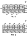
- FIG. 5 illustrates the SOI wafer of FIG. 4 with the plurality of shallow isolation trenches filled with an electrically insulative material in accordance with one embodiment of the present invention.
- FIG. 6 illustrates the SOI wafer of FIG. 5 once the electrically insulative material within the trenches has been planarized.
- FIG. 2 illustrates a silicon-on-insulator (SOI) wafer that can be formed by a variety of conventional methods, such as SIMOX or wafer bonding and etch back.
- the wafer 200 includes a silicon or other semiconductor substrate 202 , a buried oxide (BOX) layer 204 , and a silicon on insulator (SOI) layer 206 .
- a pad oxide layer 308 and a pad nitride layer 310 are formed over the SOI layer 206 .
- the pad oxide layer 308 is typically silicon dioxide and is approximately between 2-10 nm in thickness.
- Some embodiments of the present invention omit the pad oxide layer 308 such as when a buffer between the pad nitride layer 310 and the silicon 206 is not needed. For example, as the thickness of the pad nitride layer 310 is reduced, it causes less damage when formed over the silicon 206 . In some instances, therefore, the pad nitride layer 310 can be formed directly on the silicon 206 without the protection of the pad oxide layer 308 .
- the pad nitride layer is typically Si 3 N 4 and is approximately between 10-150 nm thick.
- a photo resist pattern can be formed on the top of the pad nitride layer 310 so as to form shallow isolation trenches down to the BOX layer 204 .
- the trenches 402 , 404 , 406 , and 408 separate a number of active areas in which separate devices, such as transistors, can be formed.
- a photo resist layer (not shown) is patterned on the pad nitride layer 310 and etching of the pad nitride layer 310 and pad oxide layer 308 is performed using the pattern.
- the photo resist can then be stripped and the resulting pattern of the pad nitride layer 310 is typically used to control the etch area of the SOI layer 206 .
- the photo resist pattern can be used as the guide for etching all three layers, as well.
- FIG. 5 depicts the SOI wafer 300 with its trenches 402 - 408 filled with oxide 502 .
- the oxide is formed by depositing silicon dioxide by means of Liquid Phase Deposition. This deposition occurs in such a manner that the oxide nucleates on, and grows from, the exposed surface of the BOX layer 204 .
- liquid-phase deposited silicon dioxide LPD-SiO 2
- LPD-SiO 2 liquid-phase deposited silicon dioxide
- silicon dioxide 502 is localized to the trenches and does not cover the active areas 504 - 512 . Furthermore, the silicon dioxide 502 in each trench is formed without seams caused by the intersection of different growth fronts and, therefore, has a uniform etch rate across its entire surface. As shown in FIG. 5 , the liquid phase deposited silicon dioxide 502 (LPD-SiO 2 ) overfills the trenches and extends above the pad nitride layer 310 by approximately 10 to 100 nm, although as much as 500 nm is contemplated.
- LPD-SiO 2 liquid phase deposited silicon dioxide 502
- LPD-SiO 2 tends to be less dense than thermally grown silicon dioxide, such as that resulting from a CVD process. Accordingly, a high temperature anneal or oxidation, such as at 800-1200° C., can be performed to densify the LPD-SiO 2 502 so that it is more characteristic of thermally grown silicon dioxide.
- the annealing step can be performed using rapid thermal annealing that lasts for seconds to minutes or a slow furnace annealing that can last for hours. In either case, the ambient atmosphere is preferably inert to slightly oxidizing. This annealing step can be performed before or after the LPD-SiO 2 502 is planarized to the level of the pad nitride layer 310 as shown in FIG.
- CMP Chemical mechanical polishing
- the thickness of the pad nitride layer 310 can be reduced as compared to conventional methods. Reducing the thickness of the pad nitride layer 310 is beneficial because it reduces the time needed to deposit the layer 310 and remove the layer 310 ; both of which are slow processes. In the past protective pad nitride layers have commonly exceeded 200 nm and more.
- the pad nitride layer 310 and possibly the pad oxide layer 308 , would be stripped off and well implantation would occur to form source/drain regions over which a gate could be constructed. Additionally, if the optional pad oxide layer 308 was omitted during fabrication, a sacrificial oxide layer can be grown over the exposed SOI regions before additional manufacturing steps are performed.
Landscapes
- Element Separation (AREA)
Abstract
Description
Claims (12)
Priority Applications (4)
| Application Number | Priority Date | Filing Date | Title |
|---|---|---|---|
| US10/732,953 US7273794B2 (en) | 2003-12-11 | 2003-12-11 | Shallow trench isolation fill by liquid phase deposition of SiO2 |
| US11/760,477 US7525156B2 (en) | 2003-12-11 | 2007-06-08 | Shallow trench isolation fill by liquid phase deposition of SiO2 |
| US11/875,069 US20080040696A1 (en) | 2003-12-11 | 2007-10-19 | Design Structures Incorporating Shallow Trench Isolation Filled by Liquid Phase Deposition of SiO2 |
| US12/112,549 US20080197448A1 (en) | 2003-12-11 | 2008-04-30 | SHALLOW TRENCH ISOLATION FILL BY LIQUID PHASE DEPOSITION OF SiO2 |
Applications Claiming Priority (1)
| Application Number | Priority Date | Filing Date | Title |
|---|---|---|---|
| US10/732,953 US7273794B2 (en) | 2003-12-11 | 2003-12-11 | Shallow trench isolation fill by liquid phase deposition of SiO2 |
Related Child Applications (1)
| Application Number | Title | Priority Date | Filing Date |
|---|---|---|---|
| US11/760,477 Division US7525156B2 (en) | 2003-12-11 | 2007-06-08 | Shallow trench isolation fill by liquid phase deposition of SiO2 |
Publications (2)
| Publication Number | Publication Date |
|---|---|
| US20050130387A1 US20050130387A1 (en) | 2005-06-16 |
| US7273794B2 true US7273794B2 (en) | 2007-09-25 |
Family
ID=34652970
Family Applications (3)
| Application Number | Title | Priority Date | Filing Date |
|---|---|---|---|
| US10/732,953 Expired - Fee Related US7273794B2 (en) | 2003-12-11 | 2003-12-11 | Shallow trench isolation fill by liquid phase deposition of SiO2 |
| US11/760,477 Expired - Fee Related US7525156B2 (en) | 2003-12-11 | 2007-06-08 | Shallow trench isolation fill by liquid phase deposition of SiO2 |
| US12/112,549 Abandoned US20080197448A1 (en) | 2003-12-11 | 2008-04-30 | SHALLOW TRENCH ISOLATION FILL BY LIQUID PHASE DEPOSITION OF SiO2 |
Family Applications After (2)
| Application Number | Title | Priority Date | Filing Date |
|---|---|---|---|
| US11/760,477 Expired - Fee Related US7525156B2 (en) | 2003-12-11 | 2007-06-08 | Shallow trench isolation fill by liquid phase deposition of SiO2 |
| US12/112,549 Abandoned US20080197448A1 (en) | 2003-12-11 | 2008-04-30 | SHALLOW TRENCH ISOLATION FILL BY LIQUID PHASE DEPOSITION OF SiO2 |
Country Status (1)
| Country | Link |
|---|---|
| US (3) | US7273794B2 (en) |
Cited By (5)
| Publication number | Priority date | Publication date | Assignee | Title |
|---|---|---|---|---|
| US20070228510A1 (en) * | 2003-12-11 | 2007-10-04 | International Business Machines Corporation | SHALLOW TRENCH ISOLATION FILL BY LIQUID PHASE DEPOSITION OF SiO2 |
| US20080040696A1 (en) * | 2003-12-11 | 2008-02-14 | International Business Machines Corporation | Design Structures Incorporating Shallow Trench Isolation Filled by Liquid Phase Deposition of SiO2 |
| US20090243000A1 (en) * | 2008-03-26 | 2009-10-01 | Anderson Brent A | Method, structure and design structure for customizing history effects of soi circuits |
| US20090243029A1 (en) * | 2008-03-26 | 2009-10-01 | Anderson Brent A | Method, structure and design structure for customizing history effects of soi circuits |
| US20100230752A1 (en) * | 2009-03-13 | 2010-09-16 | International Business Machines Corporation | Soi (silicon on insulator) substrate improvements |
Families Citing this family (5)
| Publication number | Priority date | Publication date | Assignee | Title |
|---|---|---|---|---|
| US8319285B2 (en) | 2005-12-22 | 2012-11-27 | Infineon Technologies Ag | Silicon-on-insulator chip having multiple crystal orientations |
| US8399957B2 (en) * | 2011-04-08 | 2013-03-19 | International Business Machines Corporation | Dual-depth self-aligned isolation structure for a back gate electrode |
| KR102144995B1 (en) * | 2013-09-12 | 2020-08-14 | 삼성전자주식회사 | Nanopore device including graphene nanopore and method of fabricating the same |
| CN108470709A (en) * | 2018-03-29 | 2018-08-31 | 上海华力集成电路制造有限公司 | The manufacturing method of insulation structure of shallow groove |
| CN113471289B (en) * | 2021-05-19 | 2024-07-16 | 广东省大湾区集成电路与系统应用研究院 | Silicon-on-insulator substrate and preparation method and application thereof |
Citations (5)
| Publication number | Priority date | Publication date | Assignee | Title |
|---|---|---|---|---|
| US5453395A (en) * | 1994-03-21 | 1995-09-26 | United Microelectronics Corp. | Isolation technology using liquid phase deposition |
| US5770501A (en) * | 1995-12-22 | 1998-06-23 | United Microelectronics Corporation | Process of fabricating NAND-structure flash EEPROM using liquid phase deposition |
| US5851900A (en) * | 1997-04-28 | 1998-12-22 | Mosel Vitelic Inc. | Method of manufacturing a shallow trench isolation for a semiconductor device |
| US5994178A (en) * | 1997-12-31 | 1999-11-30 | Texas Instruments - Acer Incorporated | Method of fabricating CMOS transistors with a planar shallow trench isolation |
| US6511884B1 (en) * | 2001-10-09 | 2003-01-28 | Chartered Semiconductor Manufacturing Ltd. | Method to form and/or isolate vertical transistors |
Family Cites Families (51)
| Publication number | Priority date | Publication date | Assignee | Title |
|---|---|---|---|---|
| US4693781A (en) | 1986-06-26 | 1987-09-15 | Motorola, Inc. | Trench formation process |
| CA2131668C (en) * | 1993-12-23 | 1999-03-02 | Carol Galli | Isolation structure using liquid phase oxide deposition |
| US5882982A (en) | 1997-01-16 | 1999-03-16 | Vlsi Technology, Inc. | Trench isolation method |
| US5851921A (en) | 1997-04-04 | 1998-12-22 | Advanced Micro Devices, Inc. | Semiconductor device and method for forming the device using a dual layer, self-aligned silicide to enhance contact performance |
| US6077786A (en) * | 1997-05-08 | 2000-06-20 | International Business Machines Corporation | Methods and apparatus for filling high aspect ratio structures with silicate glass |
| US5849643A (en) | 1997-05-23 | 1998-12-15 | Advanced Micro Devices, Inc. | Gate oxidation technique for deep sub quarter micron transistors |
| US5867420A (en) | 1997-06-11 | 1999-02-02 | Siemens Aktiengesellschaft | Reducing oxidation stress in the fabrication of devices |
| US6100131A (en) | 1997-06-11 | 2000-08-08 | Siemens Aktiengesellschaft | Method of fabricating a random access memory cell |
| US6306722B1 (en) | 1999-05-03 | 2001-10-23 | United Microelectronics Corp. | Method for fabricating shallow trench isolation structure |
| US6015739A (en) | 1997-10-29 | 2000-01-18 | Advanced Micro Devices | Method of making gate dielectric for sub-half micron MOS transistors including a graded dielectric constant |
| US6211002B1 (en) * | 1998-01-28 | 2001-04-03 | Texas Instruments-Acer Incorporated | CMOS process for forming planarized twin wells |
| TW399327B (en) | 1998-06-09 | 2000-07-21 | United Microelectronics Corp | The manufacturing method of DRAM capacitor |
| US6037238A (en) | 1999-01-04 | 2000-03-14 | Vanguard International Semiconductor Corporation | Process to reduce defect formation occurring during shallow trench isolation formation |
| US6010948A (en) | 1999-02-05 | 2000-01-04 | Taiwan Semiconductor Manufacturing Company | Shallow trench isolation process employing a BPSG trench fill |
| US6348389B1 (en) | 1999-03-11 | 2002-02-19 | Taiwan Semiconductor Manufacturing Company | Method of forming and etching a resist protect oxide layer including end-point etch |
| US6207531B1 (en) | 1999-07-02 | 2001-03-27 | Promos Technologies, Inc. | Shallow trench isolation using UV/O3 passivation prior to trench fill |
| US6579778B1 (en) | 1999-08-10 | 2003-06-17 | Advanced Micro Devices, Inc. | Source bus formation for a flash memory using silicide |
| US6171911B1 (en) | 1999-09-13 | 2001-01-09 | Taiwan Semiconductor Manufacturing Company | Method for forming dual gate oxides on integrated circuits with advanced logic devices |
| KR100328596B1 (en) | 1999-09-15 | 2002-03-15 | 윤종용 | method for manufacturing semiconductor devices |
| US6221767B1 (en) | 1999-10-28 | 2001-04-24 | United Microelectronics Corp. | Method of fabricating a silicide landing pad |
| US6294817B1 (en) | 1999-12-13 | 2001-09-25 | Infineon Technologies Ag | Source/drain-on insulator (S/DOI) field effect transistor using oxidized amorphous silicon and method of fabrication |
| US6265271B1 (en) | 2000-01-24 | 2001-07-24 | Taiwan Semiconductor Manufacturing Company | Integration of the borderless contact salicide process |
| US6335249B1 (en) | 2000-02-07 | 2002-01-01 | Taiwan Semiconductor Manufacturing Company | Salicide field effect transistors with improved borderless contact structures and a method of fabrication |
| US6544860B1 (en) | 2000-03-06 | 2003-04-08 | Koninklijke Philips Electronics N.V. | Shallow trench isolation method for forming rounded bottom trench corners |
| US6225167B1 (en) | 2000-03-13 | 2001-05-01 | Taiwan Semiconductor Manufacturing Company | Method of generating multiple oxide thicknesses by one oxidation step using NH3 nitridation followed by re-oxidation |
| US6541382B1 (en) | 2000-04-17 | 2003-04-01 | Taiwan Semiconductor Manufacturing Company | Lining and corner rounding method for shallow trench isolation |
| US6511887B1 (en) | 2000-06-19 | 2003-01-28 | Taiwan Semiconductor Manufacturing Computer | Method for making FET gate oxides with different thicknesses using a thin silicon nitride layer and a single oxidation step |
| JP2002016248A (en) | 2000-06-30 | 2002-01-18 | Mitsubishi Electric Corp | Method for manufacturing semiconductor device |
| US6406985B1 (en) | 2000-11-15 | 2002-06-18 | United Microelectronics Corp. | Method of fabricating buried contact |
| US20020106865A1 (en) * | 2001-02-05 | 2002-08-08 | Tai-Ju Chen | Method of forming shallow trench isolation |
| US7125783B2 (en) | 2001-04-18 | 2006-10-24 | Integrated Device Technology, Inc. | Dielectric anti-reflective coating surface treatment to prevent defect generation in associated wet clean |
| US6403485B1 (en) | 2001-05-02 | 2002-06-11 | Chartered Semiconductor Manufacturing Ltd | Method to form a low parasitic capacitance pseudo-SOI CMOS device |
| KR20020091982A (en) | 2001-06-01 | 2002-12-11 | 삼성전자 주식회사 | Non-valotile mem0ry device having sti structure and method of fabricating the same |
| US6492224B1 (en) | 2001-07-16 | 2002-12-10 | Taiwan Semiconductor Manufacturing Company | Buried PIP capacitor for mixed-mode process |
| TWI248160B (en) | 2002-01-28 | 2006-01-21 | Nanya Technology Corp | Manufacturing method of shallow trench isolation |
| US6878578B1 (en) | 2002-04-26 | 2005-04-12 | Taiwan Semiconductor Manufacturing Co., Ltd. | Method for forming a high quality chemical oxide on a freshly cleaned silicon surface as a native oxide replacement |
| KR100492155B1 (en) | 2002-08-08 | 2005-06-01 | 삼성전자주식회사 | Method for forming silicide layer of semiconductor device |
| JP2004087960A (en) | 2002-08-28 | 2004-03-18 | Fujitsu Ltd | Method for manufacturing semiconductor device |
| KR100464935B1 (en) | 2002-09-17 | 2005-01-05 | 주식회사 하이닉스반도체 | Method of fabricating semiconductor device with ultra-shallow super-steep-retrograde epi-channel by Boron-fluoride compound doping |
| KR100469128B1 (en) | 2002-11-07 | 2005-01-29 | 삼성전자주식회사 | Method of forming floating gate of non-volatile memory device having self-aligned shallow trench isolation |
| US6962857B1 (en) | 2003-02-05 | 2005-11-08 | Advanced Micro Devices, Inc. | Shallow trench isolation process using oxide deposition and anneal |
| US7238588B2 (en) | 2003-01-14 | 2007-07-03 | Advanced Micro Devices, Inc. | Silicon buffered shallow trench isolation |
| US6911369B2 (en) | 2003-02-12 | 2005-06-28 | Taiwan Semiconductor Manufacturing Company, Ltd. | Discontinuity prevention for SiGe deposition |
| US6967130B2 (en) | 2003-06-20 | 2005-11-22 | Taiwan Semiconductor Manufacturing Company, Ltd. | Method of forming dual gate insulator layers for CMOS applications |
| KR100510379B1 (en) | 2003-07-31 | 2005-08-25 | 동부아남반도체 주식회사 | Method for forming shallow trench isolation |
| US6991991B2 (en) | 2003-11-12 | 2006-01-31 | United Microelectronics Corp. | Method for preventing to form a spacer undercut in SEG pre-clean process |
| US7273794B2 (en) * | 2003-12-11 | 2007-09-25 | International Business Machines Corporation | Shallow trench isolation fill by liquid phase deposition of SiO2 |
| US20080040696A1 (en) * | 2003-12-11 | 2008-02-14 | International Business Machines Corporation | Design Structures Incorporating Shallow Trench Isolation Filled by Liquid Phase Deposition of SiO2 |
| US7087497B2 (en) | 2004-03-04 | 2006-08-08 | Applied Materials | Low-thermal-budget gapfill process |
| US7180116B2 (en) | 2004-06-04 | 2007-02-20 | Taiwan Semiconductor Manufacturing Co., Ltd. | Self-aligned metal electrode to eliminate native oxide effect for metal insulator semiconductor (MIS) capacitor |
| US7268048B2 (en) | 2004-08-06 | 2007-09-11 | Chartered Semiconductor Manufacturing Ltd. | Methods for elimination of arsenic based defects in semiconductor devices with isolation regions |
-
2003
- 2003-12-11 US US10/732,953 patent/US7273794B2/en not_active Expired - Fee Related
-
2007
- 2007-06-08 US US11/760,477 patent/US7525156B2/en not_active Expired - Fee Related
-
2008
- 2008-04-30 US US12/112,549 patent/US20080197448A1/en not_active Abandoned
Patent Citations (5)
| Publication number | Priority date | Publication date | Assignee | Title |
|---|---|---|---|---|
| US5453395A (en) * | 1994-03-21 | 1995-09-26 | United Microelectronics Corp. | Isolation technology using liquid phase deposition |
| US5770501A (en) * | 1995-12-22 | 1998-06-23 | United Microelectronics Corporation | Process of fabricating NAND-structure flash EEPROM using liquid phase deposition |
| US5851900A (en) * | 1997-04-28 | 1998-12-22 | Mosel Vitelic Inc. | Method of manufacturing a shallow trench isolation for a semiconductor device |
| US5994178A (en) * | 1997-12-31 | 1999-11-30 | Texas Instruments - Acer Incorporated | Method of fabricating CMOS transistors with a planar shallow trench isolation |
| US6511884B1 (en) * | 2001-10-09 | 2003-01-28 | Chartered Semiconductor Manufacturing Ltd. | Method to form and/or isolate vertical transistors |
Cited By (13)
| Publication number | Priority date | Publication date | Assignee | Title |
|---|---|---|---|---|
| US20070228510A1 (en) * | 2003-12-11 | 2007-10-04 | International Business Machines Corporation | SHALLOW TRENCH ISOLATION FILL BY LIQUID PHASE DEPOSITION OF SiO2 |
| US20080040696A1 (en) * | 2003-12-11 | 2008-02-14 | International Business Machines Corporation | Design Structures Incorporating Shallow Trench Isolation Filled by Liquid Phase Deposition of SiO2 |
| US20080197448A1 (en) * | 2003-12-11 | 2008-08-21 | International Business Machines Corporation | SHALLOW TRENCH ISOLATION FILL BY LIQUID PHASE DEPOSITION OF SiO2 |
| US7525156B2 (en) | 2003-12-11 | 2009-04-28 | International Business Machines Corporation | Shallow trench isolation fill by liquid phase deposition of SiO2 |
| US8420460B2 (en) * | 2008-03-26 | 2013-04-16 | International Business Machines Corporation | Method, structure and design structure for customizing history effects of SOI circuits |
| US20090243029A1 (en) * | 2008-03-26 | 2009-10-01 | Anderson Brent A | Method, structure and design structure for customizing history effects of soi circuits |
| US8410554B2 (en) | 2008-03-26 | 2013-04-02 | International Business Machines Corporation | Method, structure and design structure for customizing history effects of SOI circuits |
| US20090243000A1 (en) * | 2008-03-26 | 2009-10-01 | Anderson Brent A | Method, structure and design structure for customizing history effects of soi circuits |
| US8963211B2 (en) | 2008-03-26 | 2015-02-24 | International Business Machines Corporation | Method, structure and design structure for customizing history effects of SOI circuits |
| US9286425B2 (en) | 2008-03-26 | 2016-03-15 | Globalfoundries Inc. | Method, structure and design structure for customizing history effects of SOI circuits |
| US9349852B2 (en) | 2008-03-26 | 2016-05-24 | Globalfoundries Inc. | Method, structure and design structure for customizing history effects of SOI circuits |
| US20100230752A1 (en) * | 2009-03-13 | 2010-09-16 | International Business Machines Corporation | Soi (silicon on insulator) substrate improvements |
| US8288821B2 (en) | 2009-03-13 | 2012-10-16 | International Business Machines Corporation | SOI (silicon on insulator) substrate improvements |
Also Published As
| Publication number | Publication date |
|---|---|
| US20080197448A1 (en) | 2008-08-21 |
| US20070228510A1 (en) | 2007-10-04 |
| US20050130387A1 (en) | 2005-06-16 |
| US7525156B2 (en) | 2009-04-28 |
Similar Documents
| Publication | Publication Date | Title |
|---|---|---|
| US7525156B2 (en) | Shallow trench isolation fill by liquid phase deposition of SiO2 | |
| US5989978A (en) | Shallow trench isolation of MOSFETS with reduced corner parasitic currents | |
| US9099493B2 (en) | Semiconductor device with raised source/drain and replacement metal gate | |
| US6468853B1 (en) | Method of fabricating a shallow trench isolation structure with reduced local oxide recess near corner | |
| US5858858A (en) | Annealing methods for forming isolation trenches | |
| US7915173B2 (en) | Shallow trench isolation structure having reduced dislocation density | |
| US20060205164A1 (en) | Method of forming a shallow trench isolation structure | |
| JP2007521667A (en) | Tri-gate transistor and manufacturing method thereof | |
| US5882981A (en) | Mesa isolation Refill Process for Silicon on Insulator Technology Using Flowage Oxides as the Refill Material | |
| US6130467A (en) | Shallow trench isolation with spacers for improved gate oxide quality | |
| US6165906A (en) | Semiconductor topography employing a shallow trench isolation structure with an improved trench edge | |
| US6214657B1 (en) | Semiconductor device isolation structure and fabrication method of semiconductor device using the same | |
| US6433400B1 (en) | Semiconductor fabrication employing barrier atoms incorporated at the edges of a trench isolation structure | |
| US6107140A (en) | Method of patterning gate electrode conductor with ultra-thin gate oxide | |
| US6436791B1 (en) | Method of manufacturing a very deep STI (shallow trench isolation) | |
| KR100428526B1 (en) | Method of forming an isolation oxide for silicon-on-insulator technology | |
| US20080040696A1 (en) | Design Structures Incorporating Shallow Trench Isolation Filled by Liquid Phase Deposition of SiO2 | |
| EP1109216B1 (en) | Process of making a semiconductor device having regions of insulating material formed in a semiconductor substrate | |
| US7829400B2 (en) | Semiconductor device fabrication method and semiconductor device | |
| KR100214530B1 (en) | Trench device isolation structure formation method | |
| KR100271802B1 (en) | A mothod of isolation in semicondcutor device | |
| KR100289658B1 (en) | Semiconductor Device Separation Method | |
| KR100511896B1 (en) | Method of manufacturing soi substrate | |
| KR100322533B1 (en) | Isolation method using selective epitaxial growth | |
| JP4349421B2 (en) | Manufacturing method of semiconductor device |
Legal Events
| Date | Code | Title | Description |
|---|---|---|---|
| AS | Assignment |
Owner name: INERNATIONAL BUSINESS MACHINES CORPORATION, NEW YO Free format text: ASSIGNMENT OF ASSIGNORS INTEREST;ASSIGNORS:HAKEY, MARK CHARLES;HOLMES, STEVEN JOHN;HORAK, DAVID VACLAV;AND OTHERS;REEL/FRAME:014482/0087;SIGNING DATES FROM 20031208 TO 20040324 |
|
| FEPP | Fee payment procedure |
Free format text: PAYOR NUMBER ASSIGNED (ORIGINAL EVENT CODE: ASPN); ENTITY STATUS OF PATENT OWNER: LARGE ENTITY |
|
| REMI | Maintenance fee reminder mailed | ||
| LAPS | Lapse for failure to pay maintenance fees | ||
| STCH | Information on status: patent discontinuation |
Free format text: PATENT EXPIRED DUE TO NONPAYMENT OF MAINTENANCE FEES UNDER 37 CFR 1.362 |
|
| FP | Lapsed due to failure to pay maintenance fee |
Effective date: 20110925 |
|
| AS | Assignment |
Owner name: GLOBALFOUNDRIES U.S. 2 LLC, NEW YORK Free format text: ASSIGNMENT OF ASSIGNORS INTEREST;ASSIGNOR:INTERNATIONAL BUSINESS MACHINES CORPORATION;REEL/FRAME:036550/0001 Effective date: 20150629 |
|
| AS | Assignment |
Owner name: GLOBALFOUNDRIES INC., CAYMAN ISLANDS Free format text: ASSIGNMENT OF ASSIGNORS INTEREST;ASSIGNORS:GLOBALFOUNDRIES U.S. 2 LLC;GLOBALFOUNDRIES U.S. INC.;REEL/FRAME:036779/0001 Effective date: 20150910 |