US7250658B2 - Hybrid planar and FinFET CMOS devices - Google Patents
Hybrid planar and FinFET CMOS devices Download PDFInfo
- Publication number
- US7250658B2 US7250658B2 US11/122,193 US12219305A US7250658B2 US 7250658 B2 US7250658 B2 US 7250658B2 US 12219305 A US12219305 A US 12219305A US 7250658 B2 US7250658 B2 US 7250658B2
- Authority
- US
- United States
- Prior art keywords
- finfet
- fet
- device region
- planar single
- layer
- Prior art date
- Legal status (The legal status is an assumption and is not a legal conclusion. Google has not performed a legal analysis and makes no representation as to the accuracy of the status listed.)
- Expired - Lifetime, expires
Links
Images


Classifications
-
- H—ELECTRICITY
- H10—SEMICONDUCTOR DEVICES; ELECTRIC SOLID-STATE DEVICES NOT OTHERWISE PROVIDED FOR
- H10D—INORGANIC ELECTRIC SEMICONDUCTOR DEVICES
- H10D86/00—Integrated devices formed in or on insulating or conducting substrates, e.g. formed in silicon-on-insulator [SOI] substrates or on stainless steel or glass substrates
- H10D86/201—Integrated devices formed in or on insulating or conducting substrates, e.g. formed in silicon-on-insulator [SOI] substrates or on stainless steel or glass substrates the substrates comprising an insulating layer on a semiconductor body, e.g. SOI
- H10D86/215—Integrated devices formed in or on insulating or conducting substrates, e.g. formed in silicon-on-insulator [SOI] substrates or on stainless steel or glass substrates the substrates comprising an insulating layer on a semiconductor body, e.g. SOI comprising FinFETs
-
- H—ELECTRICITY
- H10—SEMICONDUCTOR DEVICES; ELECTRIC SOLID-STATE DEVICES NOT OTHERWISE PROVIDED FOR
- H10D—INORGANIC ELECTRIC SEMICONDUCTOR DEVICES
- H10D86/00—Integrated devices formed in or on insulating or conducting substrates, e.g. formed in silicon-on-insulator [SOI] substrates or on stainless steel or glass substrates
- H10D86/01—Manufacture or treatment
- H10D86/011—Manufacture or treatment comprising FinFETs
-
- H—ELECTRICITY
- H10—SEMICONDUCTOR DEVICES; ELECTRIC SOLID-STATE DEVICES NOT OTHERWISE PROVIDED FOR
- H10D—INORGANIC ELECTRIC SEMICONDUCTOR DEVICES
- H10D30/00—Field-effect transistors [FET]
- H10D30/01—Manufacture or treatment
- H10D30/021—Manufacture or treatment of FETs having insulated gates [IGFET]
- H10D30/024—Manufacture or treatment of FETs having insulated gates [IGFET] of fin field-effect transistors [FinFET]
-
- H—ELECTRICITY
- H10—SEMICONDUCTOR DEVICES; ELECTRIC SOLID-STATE DEVICES NOT OTHERWISE PROVIDED FOR
- H10D—INORGANIC ELECTRIC SEMICONDUCTOR DEVICES
- H10D30/00—Field-effect transistors [FET]
- H10D30/60—Insulated-gate field-effect transistors [IGFET]
- H10D30/62—Fin field-effect transistors [FinFET]
Definitions
- the present invention relates to integrated semiconductor devices, and more particularly to an integrated semiconductor circuit that includes a planar single gate complementary metal oxide semiconductor (CMOS) device; and a double gate device, i.e., FinFET, which are fabricated on the same semiconductor substrate.
- CMOS complementary metal oxide semiconductor
- FinFET double gate device
- the planar single gate CMOS device is an nFET formed on a thin silicon-on-insulator (SOI) layer
- the FinFET is a pFinFET structure having a vertical channel that has a surface orientation at the ( 110 ) direction.
- the planar single gate CMOS device is a pFET formed on a thin SOI layer with a ( 110 ) surface orientation and the FinFET is an nFinFET structure having a vertical channel that has a surface ( 100 ) orientation.
- the present invention also provides a method for fabricating the integrated semiconductor circuit of the present invention.
- CMOS complementary metal oxide semiconductor
- Electrons are known to have a high mobility for a ( 100 ) Si surface orientation, but holes are known to have high mobility for a ( 110 ) surface orientation. That is, hole mobility values on ( 100 ) Si are roughly 2 ⁇ -4 ⁇ lower than the corresponding electron hole mobility for this crystallographic orientation.
- pFETs are typically designed with larger widths In order to balance pull-up currents against the nFET pull-down currents and achieve uniform circuit switching; nFETs with larger widths are undesirable since they take up a significant amount of chip area.
- hole mobilities on ( 110 ) Si are 2 ⁇ higher than on ( 100 ) Si; therefore, pFETs formed on a ( 110 ) surface will exhibit significantly higher drive currents than pF Ts formed on a ( 100 ) surface.
- electron mobilities on ( 110 ) Si surfaces are significantly degraded compared to ( 100 ) Si surfaces.
- a FinFET is a double-gated device that comprises a tall, yet thin vertical channel region.
- a wafer with a ( 100 ) surface orientation can be used to fabricate FinFETs with a ( 110 ) channel surface orientation.
- the pFinFET experiences enhanced mobility with respect to the conventional CMOS device fabricated on a wafer with a ( 100 ) surface orientation.
- the nFinFET fabricate on the ( 100 ) surface orientation experiences mobility degradation compared to a conventional nFET on the ( 100 ) surface channel orientation.
- planar single gated devices or different types of double gated devices on a semiconductor wafer
- both planar and FinFET devices on the same wafer in such a fashion that the devices are formed with a surface orientation that enhances the performance of each device.
- the pFinFET should be fabricated such that the structure has a surface channel that is oriented at the ( 110 ) direction.
- a circuit that is comprised of an nFinFET fabricated on a wafer with a ( 110 ) surface orientation so that the nFinFET has a ( 100 ) surface orientation and a planar pFET device having a ( 110 ) surface orientation.
- One object of the present invention is to provide an integrated semiconductor circuit that includes at least one FinFET device and at least one planar single gated FET device on the same semiconductor substrate.
- a further object of the present invention is to provide an integrated semiconductor circuit that includes at least one FinFET device and at least one planar single gated FET device that are fabricated on the same semiconductor substrate in a manner such that each device is oriented in a direction that enhances the performance of the device.
- a still further object of the present invention is to provide an integrated semiconductor circuit that comprises an nFET and a pFinFET wherein the pFinFET structure has a ( 110 ) surface orientation and the nFET has a ( 100 ) surface orientation.
- An additional object of the present invention is to provide an integrated semiconductor circuit that comprises a pFET and an nFinFET wherein the pFET structure has a ( 110 ) surface orientation.
- Another object of the present invention is to provide a simple, yet easy method for providing hybrid planar and FinFET CMOS devices.
- a method in which resist imaging and a patterned hard mask are used in trimming the width of the FinFET active device region and subsequent resist imaging and etching are used in thinning the thickness of the FET device area is used in thinning the thickness of the FET device area.
- the trimmed active FinFET device region is formed such that it lies perpendicular to the thinned FET device region.
- the FinFET device region is formed such that it is oriented in the ( 110 ) direction, while the thinned FET device region is oriented in the ( 100 ) direction.
- the substrate is a ( 110 ) surface orientated wafer and the FinFET has a ( 100 ) surface orientation, while the planar single gated device has a ( 110 ) surface orientation.
- the method of the present invention comprises the steps of:
- a silicon-on-insulator structure comprising at least a top semiconductor layer located on a buried insulating layer, said top semiconductor layer having at least one patterned hard mask located in a FinFET region of the structure and at least one patterned hard mask located in a FET region of the structure;
- etching exposed portions of the top semiconductor that are not protected with said hard masks stopping on said buried insulating layer said etching defining a FinFET active device region and a FET active device region, said FinFET active device region being perpendicular to the FET active device region;
- the present invention also relates to an integrated semiconductor circuit that comprises at least one pFinFET and at least one nFET located atop a buried insulating layer of an silicon-on-insulator substrate, said at least one nFET is located on a surface of a top semiconductor layer of the silicon-on-insulator substrate and said at least one pFinFET has a vertical channel that is perpendicular to the at least one nFET.
- the integrated semiconductor circuit comprises at least one nFinFET and at least one pFET located atop a buried insulating layer of an silicon-on-insulator substrate, said at least one pFET is located on a surface of a top semiconductor layer of the silicon-on-insulator substrate and said at least one nFinFET has a vertical channel that is perpendicular to the at least one pFET.
- the integrated semiconductor circuit of the present invention comprises at least one FinFET and at least one planar single gated FET located atop a buried insulating layer of an silicon-on-insulator substrate, said at least one planar single gated FET comprising an active device region that includes a patterned top semiconductor layer of the silicon-on-insulator substrate and said at least-one FinFET has a vertical channel that is perpendicular to the at least one planar single gated FET.
- FIG. 1 is a pictorial representation (through a cross sectional view) illustrating a starting SOI substrate employed in the present invention.
- FIG. 2 is a pictorial representation (through a cross sectional view) illustrating a structure containing an oxide layer on an upper surface of the SOI substrate of FIG. 1 .
- FIG. 3 is a pictorial representation (through a cross sectional view) illustrating a structure containing a cap layer located atop the structure shown in FIG. 2 .
- FIG. 4 is a pictorial representation (through a cross sectional illustrating a structure after lithography is used to form resist images for defining active device regions.
- FIG. 5 is a pictorial representation (through a cross sectional view) illustrating a structure after the cap layer and the oxide layer are etched selective to the resist images.
- FIG. 6 is a pictorial representation (through a cross sectional view) illustrating a structure after removing the resist images and forming a resist image blocking the FET device region.
- FIG. 7 is a pictorial representation (through a cross sectional view) illustrating a structure after the FinFET hard mask has been trimmed.
- FIG. 8 is a pictorial representation (through a cross sectional view) illustrating a structure after removing the blocking mask and etching the exposed surfaces of the top semiconductor layer of the SOI substrate forming FinFET and FET active device regions.
- FIG. 9 is a pictorial representation (through a cross sectional view) illustrating a structure after blocking the FinFET active device region and removing the hard mask from the FET device region.
- FIG. 10 is a pictorial representation (through a cross sectional view) illustrating a structure after the FET active device region has been thinned to a height that is less than the height of the FinFET active device region.
- FIG. 11 is a pictorial representation (through a cross sectional view) illustrating a structure after a gate dielectric has been formed on vertical surfaces of the FinFET active device region and on a horizontal surface of the FET active device region.
- FIG. 12 is a pictorial representation (through a cross sectional view) illustrating a structure containing a deposited gate conductor material.
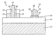
- FIG. 13 is a pictorial representation (through a cross section perpendicular to the gate) illustrating a structure containing patterned gate electrodes.
- FIG. 14 is a pictorial representation (through a cross section perpendicular to the gate view) illustrating a final structure of the present invention.
- FIG. 1 illustrates an initial silicon-on-insulator (SOI) substrate 10 that may be used in the present invention.
- SOI substrate 10 includes a buried insulating region 14 that is positioned between a bottom semiconductor layer 12 and a top semiconductor layer 16 .
- the top semiconductor layer 16 is sometimes referred to in the art as an SOI layer of an SOI substrate.
- the SOI layer is the layer of the SOI substrate in which active devices are typically built upon.
- semiconductor as used herein to describe the bottom semiconductor layer 12 and the top semiconductor layer 16 denotes any semiconducting material including, for example, Si, Ge, SiGe, SiC, SiGeC, InAs, GaAs, InP or other like III/V compound semiconductors. Multilayers of these semiconductor s are also contemplated herein.
- both semiconductor layers, i.e., the bottom semiconductor layer 12 and the top semiconductor layer 16 of the SOI substrate 10 are both comprised of Si.
- the buried insulating layer 14 may be a crystalline or non-crystalline oxide or nitride. In a preferred embodiment of the present invention, the buried insulating layer 14 is an oxide.
- the buried insulating layer 14 may be continuous, as shown, or it may be discontinuous. When a discontinuous buried insulating region is present, the insulating region exists as isolated islands that are surrounded by semiconductor material.
- the SOI substrate 10 may be a standard ( 100 ) oriented wafer, a ( 110 ) oriented wafer, or, any other surface orientation. A preferred orientation of the SOI substrate is the ( 100 ) surface orientation.
- the SOI substrate 10 may be formed utilizing standard processes including for example, SIMOX (separation by ion implantation of oxygen) or bonding.
- SIMOX separation by ion implantation of oxygen
- bonding an optional thinning step may follow the bonding process. The optional thinning step reduces the thickness of the top semiconductor layer to a layer having a thickness that is more desirable.
- the thickness of the top semiconductor layer 16 of the SOI substrate 10 is from about 100 to about 1000 ⁇ , with a thickness of from about 500 to about 700 ⁇ being more highly preferred.
- the buried insulating layer 14 of the SOI substrate 10 has a thickness of from about 10 to about 2000 ⁇ , with a thickness of from about 1000 to about 1500 ⁇ being more highly preferred.
- the thickness of the bottom semiconductor layer 12 is inconsequential to the present invention.
- an oxide layer 18 is formed on an upper exposed surface of the top semiconductor layer 16 providing the structure shown, for example, in FIG. 2 .
- the oxide layer 18 is formed by subjecting the top semiconductor layer 16 of the SOI substrate 10 to an oxidation process.
- the oxidation process may be performed using a wet or dry thermal oxidation process.
- the oxidation process used at this point of the present invention is typically performed at a temperature of about 1000° C. or above.
- the oxide layer 18 may be formed by a deposition process including, for example, chemical vapor deposition (CVD), plasma-assisted CVD or chemical solution deposition.
- the resultant structure including oxide layer 18 is shown, for example, in FIG. 2 .
- the thickness of the oxide layer 18 formed at this point of the present invention may vary depending on the conditions used to form the same. Typically, however, the oxide layer 18 has a thickness of from about 200 to about 800 ⁇ , with a thickness of about 400 to about 600 ⁇ being more highly preferred.
- the oxide layer 18 is employed in the present invention as a hard mask during a subsequent Si etch to define the active regions as well as a protective layer to protect the FinFET during the gate stack etch and also during the spacer etch.
- a cap layer 20 comprising silicon is deposited on an exposed upper surface of the oxide layer 18 .
- the resultant structure that is formed after depositing the cap layer 20 is shown, for example, in FIG. 3 .
- the cap layer 20 which is formed by a deposition process such as a sputter etch process, is used to protect the oxide layer 18 during the FinFET trimming process.
- the cap layer 20 is typically thinner than the oxide layer 18 .
- the cap layer 20 has a thickness of from about 10 to about 500 ⁇ , with a thickness of from about 50 to about 100 ⁇ being more highly preferred.
- lithography is used to pattern resist images for the pFinFET active device region and nFET active device region, or alternatively nFinFET and pFET.
- patterned resist image 22 (which defines the FinFET active device region) and patterned resist image 24 (which defines the FET active device region) are formed on predetermined portions of the cap layer 20 .
- the patterned resist images 22 and 24 are formed by first applying a photoresist to the entire surface of cap layer 20 , then exposing the photoresist to a desire radiation pattern, and thereafter developing the pattern into the exposed photoresist utilizing a conventional resist developer.
- the structure including the patterned photoresist images 22 and 24 is shown, for example, in FIG. 4 .
- the cap layer 20 and the oxide layer 18 not protected by the resist images 22 and 24 are etched selective to the resist images to form hard mask patterns for the FinFET active region and the FET active region, respectively.
- the etching used in this step of the present invention is a directional reactive ion etch process or similar dry etch process that is capable of removing the cap layer 20 and the oxide layer 18 stopping on an upper surface of the top semiconductor layer 16 .
- the resultant structure that is formed after this step of the present invention has been performed is shown, for example, in FIG. 5 .
- the resist images 22 and 24 are removed using a wet solvent stripping process or a standard ashing process known to those skilled in the art so as to expose hard mask pattern 26 and hard mask pattern 28 .
- Hard mask pattern 26 is used in the present invention to define the active area for the FinFET, whereas hard mask pattern 28 is used in defining the active area for the planar single gated FET.
- a resist mask 30 is then formed in the region in which the planar single gated FET will be formed to provide the structure shown in FIG. 6 .
- the resist mask 30 covers the hard mask pattern 28 as well as portions of the top semiconductor layer 16 abutting the hard mask pattern 28 .
- Resist mask 30 is formed by applying a photoresist to the structure shown in FIG. 5 , and thereafter patterning the applied photoresist using lithography.
- the hard mask pattern 26 is then selectively trimmed using a chemical oxide removal process.
- the chemical oxide removal (COR) processing step comprises exposing the structure to a gaseous mixture of HF and ammonia at a pressure of about 30 mTorr or below, preferably at a pressure between about 1 mTorr and about 10 mTorr, and a temperature of about 25° C. or a temperature slightly above room temperature.
- the ratio of gaseous HF to gaseous ammonia is from about 1:10 to about 10:1, with a ratio of about 2:1 being more highly preferred.
- the hard mask pattern 26 for the FinFET is trimmed using a wet etch process in which a chemical etchant, such as hydrofluoric acid, that selectively removes oxide is employed.
- a chemical etchant such as hydrofluoric acid
- the resultant structure that is formed after the trimming step has been performed is shown, for example, in FIG. 7 .
- the oxide layer 18 of the hard mask pattern 26 is thinner than the overlying patterned cap layer 20 as well as the oxide layer of the hard mask pattern 28 .
- the resist mask 30 that blocked the FET device region is removed utilizing a conventional stripping process.
- a dry etching process such as reactive ion etching, plasma etching, ion beam etching or laser ablation is employed to etch the active regions for the FinFET and the FET.
- a dry etching process is employed to remove the cap layer 20 as well as the top semiconductor layer 16 that are not protected by either the trimmed hard mask pattern 26 or the hard mask pattern 28 .
- the etching step used at this point of the present invention thus removes any unprotected silicon (or semiconductor material) from the structure stopping on buried insulating layer 14 .
- the resultant structure is shown in FIG. 8 .
- reference numeral 32 denotes the active device region for the FinFET
- reference numeral 34 denotes the active device region for the planar single gated FET (p or n).
- Portions of the FinFET active device region will serve as the channel region of the FinFET (p or N).
- the channel region of the pFinFET has a ( 110 ) surface orientation.
- the FinFET is an nFinFET having a ( 100 ) surface orientation
- the planar single gated device is a pFET having a ( 110 ) surface orientation.
- Another resist mask 36 is patterned over the FinFET region using a standard lithography process.
- an etching process is used to selectively remove the oxide layer 18 of the patterned hard mask 28 over the FET active device region 34 .
- the etching process used to remove the oxide layer 18 of the patterned hard mask 28 from the FET active; device region 34 may include a wet chemical etching processor a dry etching process.
- the resultant structure after resist mask 36 formation and etching the patterned oxide layer 18 from the FET device region 34 is shown, for example, in FIG. 9 .
- the FET device region 34 may be thinned using an etching process that is highly selective to SiO 2 . Alternatively, the resist mask may be left in place during the thinning process. The thinned FET active device region 34 is shown in FIG. 10 .
- the resist mask 36 is removed from the structure utilizing a conventional resist stripping process. It is noted that at this point of the present invention, the FinFET active device region 32 has a height, h 1 , that is greater than the height, h 2 , of the FET active device region 34 . Another feature of the structure at this point of the present invention is that the FinFET active device region is perpendicular to the FET active device region.
- the FinFET has a ( 110 ) surface orientation if the starting wafer has a ( 100 ) surface orientation. If the starting wafer has a ( 110 ) surface orientation, then the FinFET has a ( 100 ) surface orientation.
- An oxidation process is carried out to form a sacrificial oxide layer (not shown in the drawings) to remove any damaged semiconductor layers from the active regions of the FinFET and the FET.
- the thickness of the sacrificial oxide layer formed at this point of the present invention may vary depending on the conditions of the oxidation process itself. Typically, however, the sacrificial oxide layer has a thickness of from about 30 to about 100 ⁇ .
- a block mask not shown, may be patterned over the FET region and an ion implantation process may be performed to implant the FinFET channel regions to set the threshold voltage of the device. A similar procedure may be performed to set the threshold voltage of the FET device. A conventional anneal process is then typically performed to activate the dopants.
- the sacrificial oxide layer is then removed from the structure using a wet or dry etching process.
- a gate dielectric 40 is formed on the exposed vertical surfaces of the FinFET active device region 32 and the exposed horizontal surface of the FET active device region 34 .
- the gate dielectric 40 may comprise an oxide, nitride, oxynitride or any combination thereof.
- the gate dielectric 40 is an oxide such as, but not limited to: SiO 2 , Al 2 O 2 , perovskite oxides, or other like oxides.
- the gate dielectric 40 is formed utilizing a thermal oxidation, nitridation, or oxynitridation process.
- the thickness of the gate dielectric 40 is from about 0.5 to about 10 nm, with a thickness of from about 0.8 to about 1-0 nm being more highly preferred.
- the structure including the gate dielectric 40 is shown, for example, in FIG. 11 .
- the FinFET active device region 32 has two gate dielectrics formed on the exposed vertical surfaces, while the FET active device 34 has a single gate dielectric formed on the exposed horizontal surface thereof.
- a gate conductor material 42 is then formed over the entire structure shown in FIG. 11 providing the structure shown, for example, in FIG. 12 .
- the gate, conductor material 42 is formed utilizing a conventional deposition process such as, for example, chemical vapor deposition (CVD), plasma-assisted CVD, evaporation, sputtering, chemical solution deposition, or atomic layer deposition.
- the gate conductor material 42 may comprise poly-Si; an elemental metal such as W; an alloy containing one or more elemental metals; a silicide; or a stack combination thereof, such as, for example, poly-Si/W or silicide.
- FIG. 13 which is a cross sectional view perpendicular to the gate, the patterned gate electrode for the FinFET is labeled as 44 , while the patterned gate electrode for the FET is labeled as 46 .
- a hard mask over the gate electrode regions before the gate stack etch.
- the hard mask for the FinFET gate may be blocked using a lithography mask, and the FET gate stack may be etched selectively with respect to the lithography mask. The process may be repeated to etch the gate stack for the FinFET.
- a resist mask is patterned over the FET region and a low energy ion implant process (on the order of 20 KeV or less) is used to implant, if desired, halo implants as well as extension implants for the FinFET region.
- a typical implant species for the optional FinFET halo implant may be arsenic.
- a typical implant for the FinFET extension may be boron or BF 2 , if the FinFET is a p-type device.
- the resist mask is removed using a solvent stripping process or an oxygen ash process.
- Another resist mask (not shown) is next patterned over the FinFET region and the FET halo, if desired, and FET extensions are implanted using boron or indium for the optional halo implant, and arsenic for the FET extension in the case that the planar single gated FET is an nFET.
- the resist mask is removed using a conventional resist removal process.
- a dielectric material such as an oxide, nitride, oxynitride or any combination thereof, is deposited and a directional etching process is used to from source/drain spacers.
- a directional etching process is used to from source/drain spacers.
- An independent spacer etch process may be performed by using a resist mask to cover the FET, while the FinFET spacers 48 are formed and the FinFET may be protected by another resist mask while the FET spacers 50 are formed.
- the resultant structure including source/drain spacers 48 and 50 is shown, for example, in FIG. 14 .
- the source/drain implants are then formed for the FinFET and the FET using a conventional block mask and ion implantation.
- a layer of selective epitaxial Si may be grown on the source/drain regions before the implant to reduce parasitic resistance.
- a conventional rapid thermal anneal process may then be used to activate the junctions.
- a silicide process may be employed to create low resistance source/drain contact regions.
- a conventional interconnect process may be used to continue the process through the back end of the line.
Landscapes
- Metal-Oxide And Bipolar Metal-Oxide Semiconductor Integrated Circuits (AREA)
- Thin Film Transistor (AREA)
- Electrodes Of Semiconductors (AREA)
- Solid State Image Pick-Up Elements (AREA)
Abstract
Description
Claims (6)
Priority Applications (1)
| Application Number | Priority Date | Filing Date | Title |
|---|---|---|---|
| US11/122,193 US7250658B2 (en) | 2003-06-26 | 2005-05-04 | Hybrid planar and FinFET CMOS devices |
Applications Claiming Priority (2)
| Application Number | Priority Date | Filing Date | Title |
|---|---|---|---|
| US10/604,097 US6911383B2 (en) | 2003-06-26 | 2003-06-26 | Hybrid planar and finFET CMOS devices |
| US11/122,193 US7250658B2 (en) | 2003-06-26 | 2005-05-04 | Hybrid planar and FinFET CMOS devices |
Related Parent Applications (1)
| Application Number | Title | Priority Date | Filing Date |
|---|---|---|---|
| US10/604,097 Division US6911383B2 (en) | 2003-06-26 | 2003-06-26 | Hybrid planar and finFET CMOS devices |
Publications (2)
| Publication Number | Publication Date |
|---|---|
| US20050263831A1 US20050263831A1 (en) | 2005-12-01 |
| US7250658B2 true US7250658B2 (en) | 2007-07-31 |
Family
ID=33539887
Family Applications (2)
| Application Number | Title | Priority Date | Filing Date |
|---|---|---|---|
| US10/604,097 Expired - Fee Related US6911383B2 (en) | 2003-06-26 | 2003-06-26 | Hybrid planar and finFET CMOS devices |
| US11/122,193 Expired - Lifetime US7250658B2 (en) | 2003-06-26 | 2005-05-04 | Hybrid planar and FinFET CMOS devices |
Family Applications Before (1)
| Application Number | Title | Priority Date | Filing Date |
|---|---|---|---|
| US10/604,097 Expired - Fee Related US6911383B2 (en) | 2003-06-26 | 2003-06-26 | Hybrid planar and finFET CMOS devices |
Country Status (4)
| Country | Link |
|---|---|
| US (2) | US6911383B2 (en) |
| JP (1) | JP4006419B2 (en) |
| CN (1) | CN1292473C (en) |
| TW (1) | TWI283018B (en) |
Cited By (107)
| Publication number | Priority date | Publication date | Assignee | Title |
|---|---|---|---|---|
| US20060275988A1 (en) * | 2005-06-03 | 2006-12-07 | Atsushi Yagishita | Semiconductor device and method of fabricating the same |
| US20070194373A1 (en) * | 2006-02-22 | 2007-08-23 | Anderson Brent A | Cmos structure and method including multiple crystallographic planes |
| US20070221956A1 (en) * | 2006-03-23 | 2007-09-27 | Kabushiki Kaisha Toshiba | Semiconductor device and method of fabricating the same |
| US20090057765A1 (en) * | 2007-08-30 | 2009-03-05 | International Business Machines Corporation | Finfet structure using differing gate dielectric materials and gate electrode materials |
| US20090166739A1 (en) * | 2005-12-02 | 2009-07-02 | Tohoku University | Semiconductor Device |
| US20100270621A1 (en) * | 2009-04-23 | 2010-10-28 | Nec Electronics Corporation | Semiconductor device and method of manufacturing the semiconductor device |
| US8278184B1 (en) | 2011-11-02 | 2012-10-02 | United Microelectronics Corp. | Fabrication method of a non-planar transistor |
| US8426277B2 (en) | 2011-09-23 | 2013-04-23 | United Microelectronics Corp. | Semiconductor process |
| US8426283B1 (en) | 2011-11-10 | 2013-04-23 | United Microelectronics Corp. | Method of fabricating a double-gate transistor and a tri-gate transistor on a common substrate |
| US8440511B1 (en) | 2011-11-16 | 2013-05-14 | United Microelectronics Corp. | Method for manufacturing multi-gate transistor device |
| US8441072B2 (en) | 2011-09-02 | 2013-05-14 | United Microelectronics Corp. | Non-planar semiconductor structure and fabrication method thereof |
| US8466502B2 (en) | 2011-03-24 | 2013-06-18 | United Microelectronics Corp. | Metal-gate CMOS device |
| US8470714B1 (en) | 2012-05-22 | 2013-06-25 | United Microelectronics Corp. | Method of forming fin structures in integrated circuits |
| US8477006B2 (en) | 2011-08-30 | 2013-07-02 | United Microelectronics Corp. | Resistor and manufacturing method thereof |
| US8497198B2 (en) | 2011-09-23 | 2013-07-30 | United Microelectronics Corp. | Semiconductor process |
| US8501636B1 (en) | 2012-07-24 | 2013-08-06 | United Microelectronics Corp. | Method for fabricating silicon dioxide layer |
| US8507350B2 (en) | 2011-09-21 | 2013-08-13 | United Microelectronics Corporation | Fabricating method of semiconductor elements |
| US8536072B2 (en) | 2012-02-07 | 2013-09-17 | United Microelectronics Corp. | Semiconductor process |
| US8569158B2 (en) | 2011-03-31 | 2013-10-29 | Tokyo Electron Limited | Method for forming ultra-shallow doping regions by solid phase diffusion |
| US8575708B2 (en) | 2011-10-26 | 2013-11-05 | United Microelectronics Corp. | Structure of field effect transistor with fin structure |
| US8580664B2 (en) | 2011-03-31 | 2013-11-12 | Tokyo Electron Limited | Method for forming ultra-shallow boron doping regions by solid phase diffusion |
| US8604548B2 (en) | 2011-11-23 | 2013-12-10 | United Microelectronics Corp. | Semiconductor device having ESD device |
| US8664060B2 (en) | 2012-02-07 | 2014-03-04 | United Microelectronics Corp. | Semiconductor structure and method of fabricating the same |
| US8674433B2 (en) | 2011-08-24 | 2014-03-18 | United Microelectronics Corp. | Semiconductor process |
| US8691651B2 (en) | 2011-08-25 | 2014-04-08 | United Microelectronics Corp. | Method of forming non-planar FET |
| US8691652B2 (en) | 2012-05-03 | 2014-04-08 | United Microelectronics Corp. | Semiconductor process |
| US8698199B2 (en) | 2012-01-11 | 2014-04-15 | United Microelectronics Corp. | FinFET structure |
| US8709901B1 (en) | 2013-04-17 | 2014-04-29 | United Microelectronics Corp. | Method of forming an isolation structure |
| US8710596B2 (en) | 2011-05-13 | 2014-04-29 | United Microelectronics Corp. | Semiconductor device |
| US8709910B2 (en) | 2012-04-30 | 2014-04-29 | United Microelectronics Corp. | Semiconductor process |
| US8722501B2 (en) | 2011-10-18 | 2014-05-13 | United Microelectronics Corp. | Method for manufacturing multi-gate transistor device |
| US8753902B1 (en) | 2013-03-13 | 2014-06-17 | United Microelectronics Corp. | Method of controlling etching process for forming epitaxial structure |
| US8766319B2 (en) | 2012-04-26 | 2014-07-01 | United Microelectronics Corp. | Semiconductor device with ultra thin silicide layer |
| US8772860B2 (en) | 2011-05-26 | 2014-07-08 | United Microelectronics Corp. | FINFET transistor structure and method for making the same |
| US8796695B2 (en) | 2012-06-22 | 2014-08-05 | United Microelectronics Corp. | Multi-gate field-effect transistor and process thereof |
| US8802521B1 (en) | 2013-06-04 | 2014-08-12 | United Microelectronics Corp. | Semiconductor fin-shaped structure and manufacturing process thereof |
| US8803247B2 (en) | 2011-12-15 | 2014-08-12 | United Microelectronics Corporation | Fin-type field effect transistor |
| US8822284B2 (en) | 2012-02-09 | 2014-09-02 | United Microelectronics Corp. | Method for fabricating FinFETs and semiconductor structure fabricated using the method |
| US8841197B1 (en) | 2013-03-06 | 2014-09-23 | United Microelectronics Corp. | Method for forming fin-shaped structures |
| US8853015B1 (en) | 2013-04-16 | 2014-10-07 | United Microelectronics Corp. | Method of forming a FinFET structure |
| US8853013B2 (en) | 2011-08-19 | 2014-10-07 | United Microelectronics Corp. | Method for fabricating field effect transistor with fin structure |
| US8871575B2 (en) | 2011-10-31 | 2014-10-28 | United Microelectronics Corp. | Method of fabricating field effect transistor with fin structure |
| US8872280B2 (en) | 2012-07-31 | 2014-10-28 | United Microelectronics Corp. | Non-planar FET and manufacturing method thereof |
| US8877623B2 (en) | 2012-05-14 | 2014-11-04 | United Microelectronics Corp. | Method of forming semiconductor device |
| US8883621B2 (en) | 2012-12-27 | 2014-11-11 | United Microelectronics Corp. | Semiconductor structure and method of fabricating MOS device |
| US8921206B2 (en) | 2011-11-30 | 2014-12-30 | United Microelectronics Corp. | Semiconductor process |
| US8927388B2 (en) | 2012-11-15 | 2015-01-06 | United Microelectronics Corp. | Method of fabricating dielectric layer and shallow trench isolation |
| US8946031B2 (en) | 2012-01-18 | 2015-02-03 | United Microelectronics Corp. | Method for fabricating MOS device |
| US8946078B2 (en) | 2012-03-22 | 2015-02-03 | United Microelectronics Corp. | Method of forming trench in semiconductor substrate |
| US8951884B1 (en) | 2013-11-14 | 2015-02-10 | United Microelectronics Corp. | Method for forming a FinFET structure |
| US8975672B2 (en) | 2011-11-09 | 2015-03-10 | United Microelectronics Corp. | Metal oxide semiconductor transistor and manufacturing method thereof |
| US8981487B2 (en) | 2013-07-31 | 2015-03-17 | United Microelectronics Corp. | Fin-shaped field-effect transistor (FinFET) |
| US8980701B1 (en) | 2013-11-05 | 2015-03-17 | United Microelectronics Corp. | Method of forming semiconductor device |
| US8987096B2 (en) | 2012-02-07 | 2015-03-24 | United Microelectronics Corp. | Semiconductor process |
| US8993384B2 (en) | 2013-06-09 | 2015-03-31 | United Microelectronics Corp. | Semiconductor device and fabrication method thereof |
| US8993433B2 (en) | 2013-05-27 | 2015-03-31 | United Microelectronics Corp. | Manufacturing method for forming a self aligned contact |
| US9000483B2 (en) | 2013-05-16 | 2015-04-07 | United Microelectronics Corp. | Semiconductor device with fin structure and fabrication method thereof |
| US9006805B2 (en) | 2013-08-07 | 2015-04-14 | United Microelectronics Corp. | Semiconductor device |
| US9006092B2 (en) | 2011-11-03 | 2015-04-14 | United Microelectronics Corp. | Semiconductor structure having fluoride metal layer and process thereof |
| US9006107B2 (en) | 2012-03-11 | 2015-04-14 | United Microelectronics Corp. | Patterned structure of semiconductor device and fabricating method thereof |
| US9006804B2 (en) | 2013-06-06 | 2015-04-14 | United Microelectronics Corp. | Semiconductor device and fabrication method thereof |
| US9012975B2 (en) | 2012-06-14 | 2015-04-21 | United Microelectronics Corp. | Field effect transistor and manufacturing method thereof |
| US9018066B2 (en) | 2013-09-30 | 2015-04-28 | United Microelectronics Corp. | Method of fabricating semiconductor device structure |
| US9019672B2 (en) | 2013-07-17 | 2015-04-28 | United Microelectronics Corporation | Chip with electrostatic discharge protection function |
| US9048246B2 (en) | 2013-06-18 | 2015-06-02 | United Microelectronics Corp. | Die seal ring and method of forming the same |
| US9064931B2 (en) | 2012-10-11 | 2015-06-23 | United Microelectronics Corp. | Semiconductor structure having contact plug and metal gate transistor and method of making the same |
| US9064814B2 (en) | 2013-06-19 | 2015-06-23 | United Microelectronics Corp. | Semiconductor structure having metal gate and manufacturing method thereof |
| US9070710B2 (en) | 2013-06-07 | 2015-06-30 | United Microelectronics Corp. | Semiconductor process |
| US9076870B2 (en) | 2013-02-21 | 2015-07-07 | United Microelectronics Corp. | Method for forming fin-shaped structure |
| US9093565B2 (en) | 2013-07-15 | 2015-07-28 | United Microelectronics Corp. | Fin diode structure |
| US9093285B2 (en) | 2013-03-22 | 2015-07-28 | United Microelectronics Corp. | Semiconductor structure and process thereof |
| US9105685B2 (en) | 2013-07-12 | 2015-08-11 | United Microelectronics Corp. | Method of forming shallow trench isolation structure |
| US9105660B2 (en) | 2011-08-17 | 2015-08-11 | United Microelectronics Corp. | Fin-FET and method of forming the same |
| US9105582B2 (en) | 2013-08-15 | 2015-08-11 | United Microelectronics Corporation | Spatial semiconductor structure and method of fabricating the same |
| US9123810B2 (en) | 2013-06-18 | 2015-09-01 | United Microelectronics Corp. | Semiconductor integrated device including FinFET device and protecting structure |
| US9142649B2 (en) | 2012-04-23 | 2015-09-22 | United Microelectronics Corp. | Semiconductor structure with metal gate and method of fabricating the same |
| US9147747B2 (en) | 2013-05-02 | 2015-09-29 | United Microelectronics Corp. | Semiconductor structure with hard mask disposed on the gate structure |
| US9159626B2 (en) | 2012-03-13 | 2015-10-13 | United Microelectronics Corp. | FinFET and fabricating method thereof |
| US9159831B2 (en) | 2012-10-29 | 2015-10-13 | United Microelectronics Corp. | Multigate field effect transistor and process thereof |
| US9159809B2 (en) | 2012-02-29 | 2015-10-13 | United Microelectronics Corp. | Multi-gate transistor device |
| US9166024B2 (en) | 2013-09-30 | 2015-10-20 | United Microelectronics Corp. | FinFET structure with cavities and semiconductor compound portions extending laterally over sidewall spacers |
| US9190291B2 (en) | 2013-07-03 | 2015-11-17 | United Microelectronics Corp. | Fin-shaped structure forming process |
| US9196500B2 (en) | 2013-04-09 | 2015-11-24 | United Microelectronics Corp. | Method for manufacturing semiconductor structures |
| US9196352B2 (en) | 2013-02-25 | 2015-11-24 | United Microelectronics Corp. | Static random access memory unit cell structure and static random access memory unit cell layout structure |
| US9214395B2 (en) | 2013-03-13 | 2015-12-15 | United Microelectronics Corp. | Method of manufacturing semiconductor devices |
| US9230812B2 (en) | 2013-05-22 | 2016-01-05 | United Microelectronics Corp. | Method for forming semiconductor structure having opening |
| US9263287B2 (en) | 2013-05-27 | 2016-02-16 | United Microelectronics Corp. | Method of forming fin-shaped structure |
| US9263282B2 (en) | 2013-06-13 | 2016-02-16 | United Microelectronics Corporation | Method of fabricating semiconductor patterns |
| US9281303B2 (en) | 2014-05-28 | 2016-03-08 | International Business Machines Corporation | Electrostatic discharge devices and methods of manufacture |
| US9299843B2 (en) | 2013-11-13 | 2016-03-29 | United Microelectronics Corp. | Semiconductor structure and manufacturing method thereof |
| US9306032B2 (en) | 2013-10-25 | 2016-04-05 | United Microelectronics Corp. | Method of forming self-aligned metal gate structure in a replacement gate process using tapered interlayer dielectric |
| US9318567B2 (en) | 2012-09-05 | 2016-04-19 | United Microelectronics Corp. | Fabrication method for semiconductor devices |
| US9349812B2 (en) | 2013-05-27 | 2016-05-24 | United Microelectronics Corp. | Semiconductor device with self-aligned contact and method of manufacturing the same |
| US9373719B2 (en) | 2013-09-16 | 2016-06-21 | United Microelectronics Corp. | Semiconductor device |
| US9385048B2 (en) | 2013-09-05 | 2016-07-05 | United Microelectronics Corp. | Method of forming Fin-FET |
| US9401429B2 (en) | 2013-06-13 | 2016-07-26 | United Microelectronics Corp. | Semiconductor structure and process thereof |
| US9466601B2 (en) | 2013-08-12 | 2016-10-11 | Samsung Electronics Co., Ltd. | Semiconductor device and method of fabricating the same |
| US9536792B2 (en) | 2013-01-10 | 2017-01-03 | United Microelectronics Corp. | Complementary metal oxide semiconductor field effect transistor, metal oxide semiconductor field effect transistor and manufacturing method thereof |
| US9559189B2 (en) | 2012-04-16 | 2017-01-31 | United Microelectronics Corp. | Non-planar FET |
| US9564340B2 (en) | 2015-02-03 | 2017-02-07 | Samsung Electronics Co., Ltd. | Method of manufacturing semiconductor device |
| US9698229B2 (en) | 2012-01-17 | 2017-07-04 | United Microelectronics Corp. | Semiconductor structure and process thereof |
| US9711368B2 (en) | 2013-04-15 | 2017-07-18 | United Microelectronics Corp. | Sidewall image transfer process |
| US9870952B1 (en) | 2017-02-07 | 2018-01-16 | International Business Machines Corporation | Formation of VFET and finFET |
| US9899224B2 (en) | 2015-03-03 | 2018-02-20 | Tokyo Electron Limited | Method of controlling solid phase diffusion of boron dopants to form ultra-shallow doping regions |
| US20180053848A1 (en) * | 2016-03-31 | 2018-02-22 | International Business Machines Corporation | Fabrication of vertical fin transistor with multiple threshold voltages |
| US10014227B2 (en) | 2011-08-10 | 2018-07-03 | United Microelectronics Corp. | Semiconductor device having strained fin structure and method of making the same |
| US10090410B1 (en) | 2017-03-17 | 2018-10-02 | International Business Machines Corporation | Forming a combination of long channel devices and vertical transport fin field effect transistors on the same substrate |
Families Citing this family (114)
| Publication number | Priority date | Publication date | Assignee | Title |
|---|---|---|---|---|
| DE10220923B4 (en) * | 2002-05-10 | 2006-10-26 | Infineon Technologies Ag | Method for producing a non-volatile flash semiconductor memory |
| US7449719B2 (en) * | 2003-06-04 | 2008-11-11 | Tadahiro Ohmi | Semiconductor device and method of manufacturing the same |
| US7456476B2 (en) | 2003-06-27 | 2008-11-25 | Intel Corporation | Nonplanar semiconductor device with partially or fully wrapped around gate electrode and methods of fabrication |
| US7355253B2 (en) * | 2003-08-22 | 2008-04-08 | International Business Machines Corporation | Strained-channel Fin field effect transistor (FET) with a uniform channel thickness and separate gates |
| US7029958B2 (en) * | 2003-11-04 | 2006-04-18 | Advanced Micro Devices, Inc. | Self aligned damascene gate |
| US7091566B2 (en) * | 2003-11-20 | 2006-08-15 | International Business Machines Corp. | Dual gate FinFet |
| US7049662B2 (en) * | 2003-11-26 | 2006-05-23 | International Business Machines Corporation | Structure and method to fabricate FinFET devices |
| US7018551B2 (en) * | 2003-12-09 | 2006-03-28 | International Business Machines Corporation | Pull-back method of forming fins in FinFets |
| US7180134B2 (en) * | 2004-01-30 | 2007-02-20 | Taiwan Semiconductor Manufacturing Company, Ltd. | Methods and structures for planar and multiple-gate transistors formed on SOI |
| JP4852694B2 (en) * | 2004-03-02 | 2012-01-11 | 独立行政法人産業技術総合研究所 | Semiconductor integrated circuit and manufacturing method thereof |
| US7087471B2 (en) * | 2004-03-15 | 2006-08-08 | International Business Machines Corporation | Locally thinned fins |
| JP4565097B2 (en) * | 2004-04-08 | 2010-10-20 | 独立行政法人産業技術総合研究所 | Double-gate MOS transistor, double-gate CMOS transistor, and manufacturing method thereof |
| KR100618827B1 (en) * | 2004-05-17 | 2006-09-08 | 삼성전자주식회사 | Semiconductor device comprising FIFNFETT and method for manufacturing same |
| DE102005022306B4 (en) * | 2004-05-17 | 2009-12-31 | Samsung Electronics Co., Ltd., Suwon | Method for producing a semiconductor device with a Fin field effect transistor (FinFET) |
| US7291886B2 (en) * | 2004-06-21 | 2007-11-06 | International Business Machines Corporation | Hybrid substrate technology for high-mobility planar and multiple-gate MOSFETs |
| US6960509B1 (en) * | 2004-06-30 | 2005-11-01 | Freescale Semiconductor, Inc. | Method of fabricating three dimensional gate structure using oxygen diffusion |
| KR100612419B1 (en) * | 2004-10-19 | 2006-08-16 | 삼성전자주식회사 | Semiconductor device having fin transistor and planar transistor and method for forming same |
| US20060086977A1 (en) | 2004-10-25 | 2006-04-27 | Uday Shah | Nonplanar device with thinned lower body portion and method of fabrication |
| US20060177977A1 (en) * | 2005-02-08 | 2006-08-10 | The Hong Kong University Of Science And Technology | Method for patterning fins and gates in a FinFET device using trimmed hard-mask capped with imaging layer |
| US7518196B2 (en) | 2005-02-23 | 2009-04-14 | Intel Corporation | Field effect transistor with narrow bandgap source and drain regions and method of fabrication |
| KR100610421B1 (en) * | 2005-03-25 | 2006-08-08 | 주식회사 하이닉스반도체 | Manufacturing Method of Semiconductor Device |
| US7521993B1 (en) * | 2005-05-13 | 2009-04-21 | Sun Microsystems, Inc. | Substrate stress signal amplifier |
| US7858481B2 (en) | 2005-06-15 | 2010-12-28 | Intel Corporation | Method for fabricating transistor with thinned channel |
| JP5128064B2 (en) * | 2005-06-17 | 2013-01-23 | 国立大学法人東北大学 | Semiconductor device |
| US7547637B2 (en) | 2005-06-21 | 2009-06-16 | Intel Corporation | Methods for patterning a semiconductor film |
| US7279375B2 (en) | 2005-06-30 | 2007-10-09 | Intel Corporation | Block contact architectures for nanoscale channel transistors |
| KR100725951B1 (en) | 2005-08-23 | 2007-06-11 | 경북대학교 산학협력단 | CMOS element with well structure |
| US7352034B2 (en) * | 2005-08-25 | 2008-04-01 | International Business Machines Corporation | Semiconductor structures integrating damascene-body FinFET's and planar devices on a common substrate and methods for forming such semiconductor structures |
| US7737532B2 (en) * | 2005-09-06 | 2010-06-15 | Taiwan Semiconductor Manufacturing Company, Ltd. | Hybrid Schottky source-drain CMOS for high mobility and low barrier |
| US7479421B2 (en) | 2005-09-28 | 2009-01-20 | Intel Corporation | Process for integrating planar and non-planar CMOS transistors on a bulk substrate and article made thereby |
| US20070090416A1 (en) | 2005-09-28 | 2007-04-26 | Doyle Brian S | CMOS devices with a single work function gate electrode and method of fabrication |
| US7575975B2 (en) * | 2005-10-31 | 2009-08-18 | Freescale Semiconductor, Inc. | Method for forming a planar and vertical semiconductor structure having a strained semiconductor layer |
| US7615806B2 (en) * | 2005-10-31 | 2009-11-10 | Freescale Semiconductor, Inc. | Method for forming a semiconductor structure and structure thereof |
| US7547947B2 (en) * | 2005-11-15 | 2009-06-16 | International Business Machines Corporation | SRAM cell |
| US7348633B2 (en) * | 2005-11-18 | 2008-03-25 | International Business Machines Corporation | Hybrid crystallographic surface orientation substrate having one or more SOI regions and/or bulk semiconductor regions |
| KR100675290B1 (en) * | 2005-11-24 | 2007-01-29 | 삼성전자주식회사 | Method for manufacturing semiconductor device having multi-channel field effect transistor and pin field effect transistor and related device |
| US7512017B2 (en) * | 2005-12-21 | 2009-03-31 | Intel Corporation | Integration of planar and tri-gate devices on the same substrate |
| JP4490927B2 (en) * | 2006-01-24 | 2010-06-30 | 株式会社東芝 | Semiconductor device |
| JP4635897B2 (en) * | 2006-02-15 | 2011-02-23 | 株式会社東芝 | Semiconductor device and manufacturing method thereof |
| US7456055B2 (en) | 2006-03-15 | 2008-11-25 | Freescale Semiconductor, Inc. | Process for forming an electronic device including semiconductor fins |
| US7419866B2 (en) * | 2006-03-15 | 2008-09-02 | Freescale Semiconductor, Inc. | Process of forming an electronic device including a semiconductor island over an insulating layer |
| US7288483B1 (en) * | 2006-03-28 | 2007-10-30 | Tokyo Electron Limited | Method and system for patterning a dielectric film |
| KR100744137B1 (en) | 2006-04-06 | 2007-08-01 | 삼성전자주식회사 | Semiconductor device and manufacturing method thereof |
| US20090289304A1 (en) * | 2006-04-07 | 2009-11-26 | Koninklijke Philips Electronics Nv | Co-integration of multi-gate fet with other fet devices in cmos technology |
| JP2007287728A (en) * | 2006-04-12 | 2007-11-01 | Elpida Memory Inc | Semiconductor device |
| US7407890B2 (en) * | 2006-04-21 | 2008-08-05 | International Business Machines Corporation | Patterning sub-lithographic features with variable widths |
| JP5003013B2 (en) * | 2006-04-25 | 2012-08-15 | 株式会社日立製作所 | Silicon light-emitting diode, silicon phototransistor, silicon laser, and manufacturing method thereof. |
| US7436006B2 (en) * | 2006-05-19 | 2008-10-14 | International Business Machines Corporation | Hybrid strained orientated substrates and devices |
| KR101357421B1 (en) * | 2006-07-13 | 2014-02-03 | 고에키자이단호진 고쿠사이카가쿠 신고우자이단 | Transistor and semiconductor device |
| WO2008007748A1 (en) * | 2006-07-13 | 2008-01-17 | National University Corporation Tohoku University | Semiconductor device |
| KR100801315B1 (en) | 2006-09-29 | 2008-02-05 | 주식회사 하이닉스반도체 | Method of manufacturing a semiconductor device with a projection transistor |
| US7592675B2 (en) * | 2006-10-02 | 2009-09-22 | Taiwan Semiconductor Manufacutring Company, Ltd. | Partial FinFET memory cell |
| CN100539153C (en) * | 2006-10-02 | 2009-09-09 | 台湾积体电路制造股份有限公司 | Semiconductor structure and memory cell |
| JP5137378B2 (en) * | 2006-10-20 | 2013-02-06 | ルネサスエレクトロニクス株式会社 | Semiconductor device and manufacturing method thereof |
| JP2008124423A (en) * | 2006-10-20 | 2008-05-29 | Oki Electric Ind Co Ltd | Semiconductor device manufacturing method and semiconductor device |
| US7544994B2 (en) * | 2006-11-06 | 2009-06-09 | International Business Machines Corporation | Semiconductor structure with multiple fins having different channel region heights and method of forming the semiconductor structure |
| US7649243B2 (en) * | 2006-11-06 | 2010-01-19 | International Business Machines Corporation | Semiconductor structures incorporating multiple crystallographic planes and methods for fabrication thereof |
| US20080128797A1 (en) * | 2006-11-30 | 2008-06-05 | International Business Machines Corporation | Structure and method for multiple height finfet devices |
| US7772656B2 (en) * | 2006-12-14 | 2010-08-10 | International Business Machines Corporation | Combination planar FET and FinFET device |
| US20080157162A1 (en) * | 2006-12-27 | 2008-07-03 | Doyle Brian S | Method of combining floating body cell and logic transistors |
| US8017463B2 (en) * | 2006-12-29 | 2011-09-13 | Intel Corporation | Expitaxial fabrication of fins for FinFET devices |
| KR100875655B1 (en) | 2007-01-04 | 2008-12-26 | 주식회사 하이닉스반도체 | Manufacturing method of semiconductor device |
| US7781278B2 (en) * | 2007-01-18 | 2010-08-24 | International Business Machines Corporation | CMOS devices having channel regions with a V-shaped trench and hybrid channel orientations, and method for forming the same |
| US7772048B2 (en) * | 2007-02-23 | 2010-08-10 | Freescale Semiconductor, Inc. | Forming semiconductor fins using a sacrificial fin |
| US7923337B2 (en) * | 2007-06-20 | 2011-04-12 | International Business Machines Corporation | Fin field effect transistor devices with self-aligned source and drain regions |
| JP4459257B2 (en) * | 2007-06-27 | 2010-04-28 | 株式会社東芝 | Semiconductor device |
| US20090057846A1 (en) * | 2007-08-30 | 2009-03-05 | Doyle Brian S | Method to fabricate adjacent silicon fins of differing heights |
| KR20090035775A (en) * | 2007-10-08 | 2009-04-13 | 삼성전자주식회사 | Semiconductor device and method of forming the same |
| US7838913B2 (en) * | 2008-05-28 | 2010-11-23 | International Business Machines Corporation | Hybrid FET incorporating a finFET and a planar FET |
| US8362566B2 (en) | 2008-06-23 | 2013-01-29 | Intel Corporation | Stress in trigate devices using complimentary gate fill materials |
| US8241970B2 (en) | 2008-08-25 | 2012-08-14 | International Business Machines Corporation | CMOS with channel P-FinFET and channel N-FinFET having different crystalline orientations and parallel fins |
| JP5003699B2 (en) * | 2009-03-10 | 2012-08-15 | 株式会社日立製作所 | Silicon light-emitting diode, silicon phototransistor, silicon laser, and manufacturing method thereof. |
| US9337100B2 (en) * | 2009-06-03 | 2016-05-10 | Qualcomm Incorporated | Apparatus and method to fabricate an electronic device |
| US9029132B2 (en) | 2009-08-06 | 2015-05-12 | International Business Machines Corporation | Sensor for biomolecules |
| JP5356970B2 (en) * | 2009-10-01 | 2013-12-04 | ユニサンティス エレクトロニクス シンガポール プライベート リミテッド | Semiconductor device |
| US8125007B2 (en) * | 2009-11-20 | 2012-02-28 | International Business Machines Corporation | Integrated circuit including FinFET RF switch angled relative to planar MOSFET and related design structure |
| US8455334B2 (en) * | 2009-12-04 | 2013-06-04 | International Business Machines Corporation | Planar and nanowire field effect transistors |
| US9068935B2 (en) | 2010-04-08 | 2015-06-30 | International Business Machines Corporation | Dual FET sensor for sensing biomolecules and charged ions in an electrolyte |
| CN102129982A (en) * | 2010-12-29 | 2011-07-20 | 北京大学深圳研究生院 | Manufacturing method of semiconductor fine pattern and FIN body of fin field effect transistor |
| US8236634B1 (en) | 2011-03-17 | 2012-08-07 | International Business Machines Corporation | Integration of fin-based devices and ETSOI devices |
| US8778744B2 (en) * | 2011-06-24 | 2014-07-15 | Institute of Microelectronics, Chinese Academy of Sciences | Method for manufacturing semiconductor field effect transistor |
| US8759904B2 (en) * | 2011-08-24 | 2014-06-24 | GlobalFoundries, Inc. | Electronic device having plural FIN-FETs with different FIN heights and planar FETs on the same substrate |
| CN102969232B (en) * | 2011-09-01 | 2015-01-14 | 中国科学院微电子研究所 | Manufacturing method of dummy gate in gate-last process |
| CN102983073B (en) * | 2011-09-05 | 2015-12-09 | 中国科学院微电子研究所 | Manufacturing method of small-scale fin structure |
| US9406518B2 (en) * | 2011-11-18 | 2016-08-02 | Taiwan Semiconductor Manufacturing Company, Ltd. | (110) surface orientation for reducing fermi-level-pinning between high-K dielectric and group III-V compound semiconductor substrate |
| US8709888B2 (en) * | 2011-12-16 | 2014-04-29 | International Business Machines Corporation | Hybrid CMOS nanowire mesh device and PDSOI device |
| US8722472B2 (en) | 2011-12-16 | 2014-05-13 | International Business Machines Corporation | Hybrid CMOS nanowire mesh device and FINFET device |
| US8563376B2 (en) * | 2011-12-16 | 2013-10-22 | International Business Machines Corporation | Hybrid CMOS nanowire mesh device and bulk CMOS device |
| US8587068B2 (en) * | 2012-01-26 | 2013-11-19 | International Business Machines Corporation | SRAM with hybrid FinFET and planar transistors |
| US8692291B2 (en) | 2012-03-27 | 2014-04-08 | International Business Machines Corporation | Passive devices for FinFET integrated circuit technologies |
| KR20130133559A (en) * | 2012-05-29 | 2013-12-09 | 에스케이하이닉스 주식회사 | Method for fabricating semiconductor device |
| US8723268B2 (en) | 2012-06-13 | 2014-05-13 | Synopsys, Inc. | N-channel and P-channel end-to-end finFET cell architecture with relaxed gate pitch |
| US8815656B2 (en) * | 2012-09-19 | 2014-08-26 | International Business Machines Corporation | Semiconductor device and method with greater epitaxial growth on 110 crystal plane |
| US8946063B2 (en) * | 2012-11-30 | 2015-02-03 | International Business Machines Corporation | Semiconductor device having SSOI substrate with relaxed tensile stress |
| TWI570812B (en) * | 2013-03-06 | 2017-02-11 | 聯華電子股份有限公司 | Method for forming fin-shaped structure |
| CN104143514B (en) * | 2013-05-09 | 2017-09-26 | 中芯国际集成电路制造(上海)有限公司 | The forming method of multiple gate field effect transistor |
| WO2014197891A2 (en) * | 2013-06-07 | 2014-12-11 | Cornell University | Floating gate based sensor apparatus and related floating gate based sensor applications |
| TWI566273B (en) * | 2013-06-13 | 2017-01-11 | 聯華電子股份有限公司 | Method of fabricating semiconductor pattern |
| US9059020B1 (en) | 2013-12-02 | 2015-06-16 | International Business Machins Corporation | Implementing buried FET below and beside FinFET on bulk substrate |
| CN103943484B (en) * | 2014-04-28 | 2016-08-17 | 上海华力微电子有限公司 | Self aligned grid separation method |
| US9419015B1 (en) * | 2015-03-13 | 2016-08-16 | Globalfoundries Inc. | Method for integrating thin-film transistors on an isolation region in an integrated circuit and resulting device |
| US20160268256A1 (en) * | 2015-03-13 | 2016-09-15 | Qualcomm Incorporated | Complementary metal-oxide semiconductor (cmos) transistor and tunnel field-effect transistor (tfet) on a single substrate |
| CN104966672B (en) * | 2015-06-30 | 2019-01-25 | 上海华力微电子有限公司 | Fin-type field effect transistor substrate preparation method |
| US9666581B2 (en) * | 2015-08-21 | 2017-05-30 | Taiwan Semiconductor Manufacturing Company, Ltd. | FinFET with source/drain structure and method of fabrication thereof |
| US9978748B2 (en) * | 2015-12-09 | 2018-05-22 | International Business Machines Corporation | Method of cutting fins to create diffusion breaks for finFETs |
| US10026653B2 (en) * | 2015-12-16 | 2018-07-17 | International Business Machines Corporation | Variable gate lengths for vertical transistors |
| CN105655410B (en) * | 2016-04-13 | 2019-07-30 | 京东方科技集团股份有限公司 | Non-shading thin film transistor, array substrate and display device |
| US9793271B1 (en) * | 2016-04-29 | 2017-10-17 | International Business Machines Corporation | Semiconductor device with different fin pitches |
| US9916978B2 (en) | 2016-06-02 | 2018-03-13 | United Microelectronics Corporation | Method for fabricating a Fin field effect transistor (FinFET) |
| US10049944B2 (en) | 2016-10-05 | 2018-08-14 | Globalfoundries Inc. | Method of manufacturing selective nanostructures into finFET process flow |
| US10517179B2 (en) * | 2016-12-15 | 2019-12-24 | Taiwan Semiconductor Manufacturing Co., Ltd. | Material composition and methods thereof |
| US10679992B1 (en) | 2018-11-16 | 2020-06-09 | International Business Machines Corporation | Integrated device with vertical field-effect transistors and hybrid channels |
| DE102021121138B3 (en) | 2021-08-13 | 2023-02-02 | Infineon Technologies Ag | SEMICONDUCTOR DEVICES AND METHOD OF MANUFACTURING A SEMICONDUCTOR DEVICE |
| US11908743B2 (en) * | 2021-09-27 | 2024-02-20 | International Business Machines Corporation | Planar devices with consistent base dielectric |
Citations (14)
| Publication number | Priority date | Publication date | Assignee | Title |
|---|---|---|---|---|
| JPS6292361A (en) | 1985-10-17 | 1987-04-27 | Toshiba Corp | Complementary type semiconductor device |
| JPS6470748A (en) | 1987-07-14 | 1989-03-16 | Agfa Gevaert Nv | Manufacture of curled photographic film |
| JPH07183488A (en) | 1993-12-24 | 1995-07-21 | Nissan Motor Co Ltd | MOS-controlled thyristor and method of manufacturing the same |
| US6166413A (en) | 1996-02-28 | 2000-12-26 | Nec Corporation | Semiconductor device having field effect transistors different in thickness of gate electrodes and process of fabrication thereof |
| US6245615B1 (en) | 1999-08-31 | 2001-06-12 | Micron Technology, Inc. | Method and apparatus on (110) surfaces of silicon structures with conduction in the <110> direction |
| US6252284B1 (en) | 1999-12-09 | 2001-06-26 | International Business Machines Corporation | Planarized silicon fin device |
| US6300182B1 (en) | 2000-12-11 | 2001-10-09 | Advanced Micro Devices, Inc. | Field effect transistor having dual gates with asymmetrical doping for reduced threshold voltage |
| US20020014666A1 (en) | 1999-11-30 | 2002-02-07 | Tadahiro Ohmi | Semiconductor device formed on (111) surface of a si crystal and fabrication process thereof |
| US20020063292A1 (en) | 2000-11-29 | 2002-05-30 | Mark Armstrong | CMOS fabrication process utilizing special transistor orientation |
| US6413802B1 (en) | 2000-10-23 | 2002-07-02 | The Regents Of The University Of California | Finfet transistor structures having a double gate channel extending vertically from a substrate and methods of manufacture |
| US20020185676A1 (en) | 2001-05-31 | 2002-12-12 | Hisayo Momose | Semiconductor device |
| US6657259B2 (en) | 2001-12-04 | 2003-12-02 | International Business Machines Corporation | Multiple-plane FinFET CMOS |
| JP2004088101A (en) | 2002-08-26 | 2004-03-18 | Internatl Business Mach Corp <Ibm> | Integrated circuit chip and method of manufacturing the same |
| US6858478B2 (en) * | 2002-08-23 | 2005-02-22 | Intel Corporation | Tri-gate devices and methods of fabrication |
-
2003
- 2003-06-26 US US10/604,097 patent/US6911383B2/en not_active Expired - Fee Related
-
2004
- 2004-06-18 TW TW093117787A patent/TWI283018B/en not_active IP Right Cessation
- 2004-06-22 JP JP2004183756A patent/JP4006419B2/en not_active Expired - Fee Related
- 2004-06-25 CN CN200410060055.8A patent/CN1292473C/en not_active Expired - Fee Related
-
2005
- 2005-05-04 US US11/122,193 patent/US7250658B2/en not_active Expired - Lifetime
Patent Citations (15)
| Publication number | Priority date | Publication date | Assignee | Title |
|---|---|---|---|---|
| JPS6292361A (en) | 1985-10-17 | 1987-04-27 | Toshiba Corp | Complementary type semiconductor device |
| JPS6470748A (en) | 1987-07-14 | 1989-03-16 | Agfa Gevaert Nv | Manufacture of curled photographic film |
| JPH07183488A (en) | 1993-12-24 | 1995-07-21 | Nissan Motor Co Ltd | MOS-controlled thyristor and method of manufacturing the same |
| US6166413A (en) | 1996-02-28 | 2000-12-26 | Nec Corporation | Semiconductor device having field effect transistors different in thickness of gate electrodes and process of fabrication thereof |
| US20010026006A1 (en) | 1999-08-31 | 2001-10-04 | Micron Technology, Inc. | Method and apparatus on (110) surfaces of silicon structures with conduction in the <110> direction |
| US6245615B1 (en) | 1999-08-31 | 2001-06-12 | Micron Technology, Inc. | Method and apparatus on (110) surfaces of silicon structures with conduction in the <110> direction |
| US20020014666A1 (en) | 1999-11-30 | 2002-02-07 | Tadahiro Ohmi | Semiconductor device formed on (111) surface of a si crystal and fabrication process thereof |
| US6252284B1 (en) | 1999-12-09 | 2001-06-26 | International Business Machines Corporation | Planarized silicon fin device |
| US6413802B1 (en) | 2000-10-23 | 2002-07-02 | The Regents Of The University Of California | Finfet transistor structures having a double gate channel extending vertically from a substrate and methods of manufacture |
| US20020063292A1 (en) | 2000-11-29 | 2002-05-30 | Mark Armstrong | CMOS fabrication process utilizing special transistor orientation |
| US6300182B1 (en) | 2000-12-11 | 2001-10-09 | Advanced Micro Devices, Inc. | Field effect transistor having dual gates with asymmetrical doping for reduced threshold voltage |
| US20020185676A1 (en) | 2001-05-31 | 2002-12-12 | Hisayo Momose | Semiconductor device |
| US6657259B2 (en) | 2001-12-04 | 2003-12-02 | International Business Machines Corporation | Multiple-plane FinFET CMOS |
| US6858478B2 (en) * | 2002-08-23 | 2005-02-22 | Intel Corporation | Tri-gate devices and methods of fabrication |
| JP2004088101A (en) | 2002-08-26 | 2004-03-18 | Internatl Business Mach Corp <Ibm> | Integrated circuit chip and method of manufacturing the same |
Cited By (164)
| Publication number | Priority date | Publication date | Assignee | Title |
|---|---|---|---|---|
| US20060275988A1 (en) * | 2005-06-03 | 2006-12-07 | Atsushi Yagishita | Semiconductor device and method of fabricating the same |
| US7371644B2 (en) | 2005-06-03 | 2008-05-13 | Kabushiki Kaisha Toshiba | Semiconductor device and method of fabricating the same |
| US7723171B2 (en) | 2005-06-03 | 2010-05-25 | Kabushiki Kaisha Toshiba | Semiconductor device and method of fabricating the same |
| US20090166739A1 (en) * | 2005-12-02 | 2009-07-02 | Tohoku University | Semiconductor Device |
| US7800202B2 (en) | 2005-12-02 | 2010-09-21 | Tohoku University | Semiconductor device |
| US20070194373A1 (en) * | 2006-02-22 | 2007-08-23 | Anderson Brent A | Cmos structure and method including multiple crystallographic planes |
| US7473946B2 (en) * | 2006-02-22 | 2009-01-06 | International Business Machines Corporation | CMOS structure and method including multiple crystallographic planes |
| US20090111225A1 (en) * | 2006-02-22 | 2009-04-30 | International Business Machines Corporation | Cmos structure and method including multiple crystallographic planes |
| US7785955B2 (en) | 2006-02-22 | 2010-08-31 | International Business Machines Corporation | CMOS structure and method including multiple crystallographic planes |
| US20070221956A1 (en) * | 2006-03-23 | 2007-09-27 | Kabushiki Kaisha Toshiba | Semiconductor device and method of fabricating the same |
| US20090057765A1 (en) * | 2007-08-30 | 2009-03-05 | International Business Machines Corporation | Finfet structure using differing gate dielectric materials and gate electrode materials |
| US7732874B2 (en) * | 2007-08-30 | 2010-06-08 | International Business Machines Corporation | FinFET structure using differing gate dielectric materials and gate electrode materials |
| US8269271B2 (en) * | 2009-04-23 | 2012-09-18 | Renesas Electronics Corporation | Hybrid planarFET and FinFET provided on a chip |
| US20100270621A1 (en) * | 2009-04-23 | 2010-10-28 | Nec Electronics Corporation | Semiconductor device and method of manufacturing the semiconductor device |
| US8586437B2 (en) | 2009-04-23 | 2013-11-19 | Renesas Electronics Corporation | Semiconductor device and method of manufacturing the semiconductor device |
| US8466502B2 (en) | 2011-03-24 | 2013-06-18 | United Microelectronics Corp. | Metal-gate CMOS device |
| US8592271B2 (en) | 2011-03-24 | 2013-11-26 | United Microelectronics Corp. | Metal-gate CMOS device and fabrication method thereof |
| US9012316B2 (en) | 2011-03-31 | 2015-04-21 | Tokyo Electron Limited | Method for forming ultra-shallow boron doping regions by solid phase diffusion |
| US8569158B2 (en) | 2011-03-31 | 2013-10-29 | Tokyo Electron Limited | Method for forming ultra-shallow doping regions by solid phase diffusion |
| US8580664B2 (en) | 2011-03-31 | 2013-11-12 | Tokyo Electron Limited | Method for forming ultra-shallow boron doping regions by solid phase diffusion |
| US8877620B2 (en) | 2011-03-31 | 2014-11-04 | Tokyo Electron Limited | Method for forming ultra-shallow doping regions by solid phase diffusion |
| US8710596B2 (en) | 2011-05-13 | 2014-04-29 | United Microelectronics Corp. | Semiconductor device |
| US8853041B2 (en) | 2011-05-13 | 2014-10-07 | United Microelectronics Corp. | Method for fabricating semiconductor device |
| US8772860B2 (en) | 2011-05-26 | 2014-07-08 | United Microelectronics Corp. | FINFET transistor structure and method for making the same |
| US9385193B2 (en) | 2011-05-26 | 2016-07-05 | United Microelectronics Corp. | FINFET transistor structure and method for making the same |
| US10014227B2 (en) | 2011-08-10 | 2018-07-03 | United Microelectronics Corp. | Semiconductor device having strained fin structure and method of making the same |
| US9406805B2 (en) | 2011-08-17 | 2016-08-02 | United Microelectronics Corp. | Fin-FET |
| US9105660B2 (en) | 2011-08-17 | 2015-08-11 | United Microelectronics Corp. | Fin-FET and method of forming the same |
| US8853013B2 (en) | 2011-08-19 | 2014-10-07 | United Microelectronics Corp. | Method for fabricating field effect transistor with fin structure |
| US8674433B2 (en) | 2011-08-24 | 2014-03-18 | United Microelectronics Corp. | Semiconductor process |
| US8691651B2 (en) | 2011-08-25 | 2014-04-08 | United Microelectronics Corp. | Method of forming non-planar FET |
| US8477006B2 (en) | 2011-08-30 | 2013-07-02 | United Microelectronics Corp. | Resistor and manufacturing method thereof |
| US8441072B2 (en) | 2011-09-02 | 2013-05-14 | United Microelectronics Corp. | Non-planar semiconductor structure and fabrication method thereof |
| US8779513B2 (en) | 2011-09-02 | 2014-07-15 | United Microelectronics Corp. | Non-planar semiconductor structure |
| US8507350B2 (en) | 2011-09-21 | 2013-08-13 | United Microelectronics Corporation | Fabricating method of semiconductor elements |
| US8497198B2 (en) | 2011-09-23 | 2013-07-30 | United Microelectronics Corp. | Semiconductor process |
| US8426277B2 (en) | 2011-09-23 | 2013-04-23 | United Microelectronics Corp. | Semiconductor process |
| US8722501B2 (en) | 2011-10-18 | 2014-05-13 | United Microelectronics Corp. | Method for manufacturing multi-gate transistor device |
| US8575708B2 (en) | 2011-10-26 | 2013-11-05 | United Microelectronics Corp. | Structure of field effect transistor with fin structure |
| US8871575B2 (en) | 2011-10-31 | 2014-10-28 | United Microelectronics Corp. | Method of fabricating field effect transistor with fin structure |
| US8278184B1 (en) | 2011-11-02 | 2012-10-02 | United Microelectronics Corp. | Fabrication method of a non-planar transistor |
| US9006092B2 (en) | 2011-11-03 | 2015-04-14 | United Microelectronics Corp. | Semiconductor structure having fluoride metal layer and process thereof |
| US9219140B2 (en) | 2011-11-09 | 2015-12-22 | United Microelectronics Corp. | Metal oxide semiconductor transistor and manufacturing method thereof |
| US8975672B2 (en) | 2011-11-09 | 2015-03-10 | United Microelectronics Corp. | Metal oxide semiconductor transistor and manufacturing method thereof |
| US9875901B2 (en) | 2011-11-09 | 2018-01-23 | United Microelectronics Corp. | Manufacturing method of metal oxide semiconductor transistor |
| US8426283B1 (en) | 2011-11-10 | 2013-04-23 | United Microelectronics Corp. | Method of fabricating a double-gate transistor and a tri-gate transistor on a common substrate |
| US8440511B1 (en) | 2011-11-16 | 2013-05-14 | United Microelectronics Corp. | Method for manufacturing multi-gate transistor device |
| US8604548B2 (en) | 2011-11-23 | 2013-12-10 | United Microelectronics Corp. | Semiconductor device having ESD device |
| US8748278B2 (en) | 2011-11-23 | 2014-06-10 | United Microelectronics Corp. | Method for fabricating semiconductor device |
| US8921206B2 (en) | 2011-11-30 | 2014-12-30 | United Microelectronics Corp. | Semiconductor process |
| US8803247B2 (en) | 2011-12-15 | 2014-08-12 | United Microelectronics Corporation | Fin-type field effect transistor |
| US8698199B2 (en) | 2012-01-11 | 2014-04-15 | United Microelectronics Corp. | FinFET structure |
| US9698229B2 (en) | 2012-01-17 | 2017-07-04 | United Microelectronics Corp. | Semiconductor structure and process thereof |
| US8946031B2 (en) | 2012-01-18 | 2015-02-03 | United Microelectronics Corp. | Method for fabricating MOS device |
| US8536072B2 (en) | 2012-02-07 | 2013-09-17 | United Microelectronics Corp. | Semiconductor process |
| US8987096B2 (en) | 2012-02-07 | 2015-03-24 | United Microelectronics Corp. | Semiconductor process |
| US8664060B2 (en) | 2012-02-07 | 2014-03-04 | United Microelectronics Corp. | Semiconductor structure and method of fabricating the same |
| US9054187B2 (en) | 2012-02-07 | 2015-06-09 | United Microelectronics Corp. | Semiconductor structure |
| US8822284B2 (en) | 2012-02-09 | 2014-09-02 | United Microelectronics Corp. | Method for fabricating FinFETs and semiconductor structure fabricated using the method |
| US9184292B2 (en) | 2012-02-09 | 2015-11-10 | United Microelectronics Corp. | Semiconductor structure with different fins of FinFETs |
| US9159809B2 (en) | 2012-02-29 | 2015-10-13 | United Microelectronics Corp. | Multi-gate transistor device |
| US9006107B2 (en) | 2012-03-11 | 2015-04-14 | United Microelectronics Corp. | Patterned structure of semiconductor device and fabricating method thereof |
| US9159626B2 (en) | 2012-03-13 | 2015-10-13 | United Microelectronics Corp. | FinFET and fabricating method thereof |
| US9379026B2 (en) | 2012-03-13 | 2016-06-28 | United Microelectronics Corp. | Fin-shaped field-effect transistor process |
| US9214384B2 (en) | 2012-03-22 | 2015-12-15 | United Microelectronics Corp. | Method of forming trench in semiconductor substrate |
| US8946078B2 (en) | 2012-03-22 | 2015-02-03 | United Microelectronics Corp. | Method of forming trench in semiconductor substrate |
| US9923095B2 (en) | 2012-04-16 | 2018-03-20 | United Microelectronics Corp. | Manufacturing method of non-planar FET |
| US9559189B2 (en) | 2012-04-16 | 2017-01-31 | United Microelectronics Corp. | Non-planar FET |
| US9142649B2 (en) | 2012-04-23 | 2015-09-22 | United Microelectronics Corp. | Semiconductor structure with metal gate and method of fabricating the same |
| US8766319B2 (en) | 2012-04-26 | 2014-07-01 | United Microelectronics Corp. | Semiconductor device with ultra thin silicide layer |
| US8993390B2 (en) | 2012-04-26 | 2015-03-31 | United Microelectronics Corp. | Method for fabricating semiconductor device |
| US8709910B2 (en) | 2012-04-30 | 2014-04-29 | United Microelectronics Corp. | Semiconductor process |
| US8691652B2 (en) | 2012-05-03 | 2014-04-08 | United Microelectronics Corp. | Semiconductor process |
| US8877623B2 (en) | 2012-05-14 | 2014-11-04 | United Microelectronics Corp. | Method of forming semiconductor device |
| US9006091B2 (en) | 2012-05-14 | 2015-04-14 | United Microelectronics Corp. | Method of forming semiconductor device having metal gate |
| US8470714B1 (en) | 2012-05-22 | 2013-06-25 | United Microelectronics Corp. | Method of forming fin structures in integrated circuits |
| US9871123B2 (en) | 2012-06-14 | 2018-01-16 | United Microelectronics Corp. | Field effect transistor and manufacturing method thereof |
| US9012975B2 (en) | 2012-06-14 | 2015-04-21 | United Microelectronics Corp. | Field effect transistor and manufacturing method thereof |
| US8999793B2 (en) | 2012-06-22 | 2015-04-07 | United Microelectronics Corp. | Multi-gate field-effect transistor process |
| US8796695B2 (en) | 2012-06-22 | 2014-08-05 | United Microelectronics Corp. | Multi-gate field-effect transistor and process thereof |
| US8501636B1 (en) | 2012-07-24 | 2013-08-06 | United Microelectronics Corp. | Method for fabricating silicon dioxide layer |
| US9312365B2 (en) | 2012-07-31 | 2016-04-12 | United Microelectronics Corp. | Manufacturing method of non-planar FET |
| US8872280B2 (en) | 2012-07-31 | 2014-10-28 | United Microelectronics Corp. | Non-planar FET and manufacturing method thereof |
| US9318567B2 (en) | 2012-09-05 | 2016-04-19 | United Microelectronics Corp. | Fabrication method for semiconductor devices |
| US9064931B2 (en) | 2012-10-11 | 2015-06-23 | United Microelectronics Corp. | Semiconductor structure having contact plug and metal gate transistor and method of making the same |
| US9159831B2 (en) | 2012-10-29 | 2015-10-13 | United Microelectronics Corp. | Multigate field effect transistor and process thereof |
| US8927388B2 (en) | 2012-11-15 | 2015-01-06 | United Microelectronics Corp. | Method of fabricating dielectric layer and shallow trench isolation |
| US8883621B2 (en) | 2012-12-27 | 2014-11-11 | United Microelectronics Corp. | Semiconductor structure and method of fabricating MOS device |
| US10062770B2 (en) | 2013-01-10 | 2018-08-28 | United Microelectronics Corp. | Complementary metal oxide semiconductor field effect transistor, metal oxide semiconductor field effect transistor and manufacturing method thereof |
| US9536792B2 (en) | 2013-01-10 | 2017-01-03 | United Microelectronics Corp. | Complementary metal oxide semiconductor field effect transistor, metal oxide semiconductor field effect transistor and manufacturing method thereof |
| US9076870B2 (en) | 2013-02-21 | 2015-07-07 | United Microelectronics Corp. | Method for forming fin-shaped structure |
| US9196352B2 (en) | 2013-02-25 | 2015-11-24 | United Microelectronics Corp. | Static random access memory unit cell structure and static random access memory unit cell layout structure |
| US8841197B1 (en) | 2013-03-06 | 2014-09-23 | United Microelectronics Corp. | Method for forming fin-shaped structures |
| US8753902B1 (en) | 2013-03-13 | 2014-06-17 | United Microelectronics Corp. | Method of controlling etching process for forming epitaxial structure |
| US9214395B2 (en) | 2013-03-13 | 2015-12-15 | United Microelectronics Corp. | Method of manufacturing semiconductor devices |
| US9502530B2 (en) | 2013-03-13 | 2016-11-22 | United Microelectronics Corp. | Method of manufacturing semiconductor devices |
| US9449964B2 (en) | 2013-03-22 | 2016-09-20 | United Microelectronics Corp. | Semiconductor process |
| US9093285B2 (en) | 2013-03-22 | 2015-07-28 | United Microelectronics Corp. | Semiconductor structure and process thereof |
| US9196500B2 (en) | 2013-04-09 | 2015-11-24 | United Microelectronics Corp. | Method for manufacturing semiconductor structures |
| US9711368B2 (en) | 2013-04-15 | 2017-07-18 | United Microelectronics Corp. | Sidewall image transfer process |
| US8853015B1 (en) | 2013-04-16 | 2014-10-07 | United Microelectronics Corp. | Method of forming a FinFET structure |
| US9117909B2 (en) | 2013-04-16 | 2015-08-25 | United Microelectronics Corp. | Non-planar transistor |
| US8709901B1 (en) | 2013-04-17 | 2014-04-29 | United Microelectronics Corp. | Method of forming an isolation structure |
| US9331171B2 (en) | 2013-05-02 | 2016-05-03 | United Microelectronics Corp. | Manufacturing method for forming semiconductor structure |
| US9147747B2 (en) | 2013-05-02 | 2015-09-29 | United Microelectronics Corp. | Semiconductor structure with hard mask disposed on the gate structure |
| US9190497B2 (en) | 2013-05-16 | 2015-11-17 | United Microelectronics Corp. | Method for fabricating semiconductor device with loop-shaped fin |
| US9000483B2 (en) | 2013-05-16 | 2015-04-07 | United Microelectronics Corp. | Semiconductor device with fin structure and fabrication method thereof |
| US9230812B2 (en) | 2013-05-22 | 2016-01-05 | United Microelectronics Corp. | Method for forming semiconductor structure having opening |
| US9349812B2 (en) | 2013-05-27 | 2016-05-24 | United Microelectronics Corp. | Semiconductor device with self-aligned contact and method of manufacturing the same |
| US8993433B2 (en) | 2013-05-27 | 2015-03-31 | United Microelectronics Corp. | Manufacturing method for forming a self aligned contact |
| US9263287B2 (en) | 2013-05-27 | 2016-02-16 | United Microelectronics Corp. | Method of forming fin-shaped structure |
| US8802521B1 (en) | 2013-06-04 | 2014-08-12 | United Microelectronics Corp. | Semiconductor fin-shaped structure and manufacturing process thereof |
| US9281199B2 (en) | 2013-06-06 | 2016-03-08 | United Microelectronics Corp. | Method for fabricating semiconductor device with paterned hard mask |
| US9006804B2 (en) | 2013-06-06 | 2015-04-14 | United Microelectronics Corp. | Semiconductor device and fabrication method thereof |
| US9070710B2 (en) | 2013-06-07 | 2015-06-30 | United Microelectronics Corp. | Semiconductor process |
| US8993384B2 (en) | 2013-06-09 | 2015-03-31 | United Microelectronics Corp. | Semiconductor device and fabrication method thereof |
| US9318609B2 (en) | 2013-06-09 | 2016-04-19 | United Microelectronics Corp. | Semiconductor device with epitaxial structure |
| US9263282B2 (en) | 2013-06-13 | 2016-02-16 | United Microelectronics Corporation | Method of fabricating semiconductor patterns |
| US9401429B2 (en) | 2013-06-13 | 2016-07-26 | United Microelectronics Corp. | Semiconductor structure and process thereof |
| US9048246B2 (en) | 2013-06-18 | 2015-06-02 | United Microelectronics Corp. | Die seal ring and method of forming the same |
| US9349695B2 (en) | 2013-06-18 | 2016-05-24 | United Microelectronics Corp. | Semiconductor integrated device including FinFET device and protecting structure |
| US9123810B2 (en) | 2013-06-18 | 2015-09-01 | United Microelectronics Corp. | Semiconductor integrated device including FinFET device and protecting structure |
| US9064814B2 (en) | 2013-06-19 | 2015-06-23 | United Microelectronics Corp. | Semiconductor structure having metal gate and manufacturing method thereof |
| US9190291B2 (en) | 2013-07-03 | 2015-11-17 | United Microelectronics Corp. | Fin-shaped structure forming process |
| US9105685B2 (en) | 2013-07-12 | 2015-08-11 | United Microelectronics Corp. | Method of forming shallow trench isolation structure |
| US9559091B2 (en) | 2013-07-15 | 2017-01-31 | United Microelectronics Corp. | Method of manufacturing fin diode structure |
| US9455246B2 (en) | 2013-07-15 | 2016-09-27 | United Microelectronics Corp. | Fin diode structure |
| US9331064B2 (en) | 2013-07-15 | 2016-05-03 | United Microelectronics Corp. | Fin diode structure |
| US9093565B2 (en) | 2013-07-15 | 2015-07-28 | United Microelectronics Corp. | Fin diode structure |
| US9019672B2 (en) | 2013-07-17 | 2015-04-28 | United Microelectronics Corporation | Chip with electrostatic discharge protection function |
| US8981487B2 (en) | 2013-07-31 | 2015-03-17 | United Microelectronics Corp. | Fin-shaped field-effect transistor (FinFET) |
| US9337193B2 (en) | 2013-08-07 | 2016-05-10 | United Microelectronics Corp. | Semiconductor device with epitaxial structures |
| US9006805B2 (en) | 2013-08-07 | 2015-04-14 | United Microelectronics Corp. | Semiconductor device |
| US9466601B2 (en) | 2013-08-12 | 2016-10-11 | Samsung Electronics Co., Ltd. | Semiconductor device and method of fabricating the same |
| US9711506B2 (en) | 2013-08-12 | 2017-07-18 | Samsung Electronics Co., Ltd. | Semiconductor device and method of fabricating the same |
| US10177150B2 (en) | 2013-08-12 | 2019-01-08 | Samsung Electronics Co., Ltd. | Semiconductor device and method of fabricating the same |
| US9105582B2 (en) | 2013-08-15 | 2015-08-11 | United Microelectronics Corporation | Spatial semiconductor structure and method of fabricating the same |
| US9362358B2 (en) | 2013-08-15 | 2016-06-07 | United Microelectronics Corporation | Spatial semiconductor structure |
| US9385048B2 (en) | 2013-09-05 | 2016-07-05 | United Microelectronics Corp. | Method of forming Fin-FET |
| US9373719B2 (en) | 2013-09-16 | 2016-06-21 | United Microelectronics Corp. | Semiconductor device |
| US9018066B2 (en) | 2013-09-30 | 2015-04-28 | United Microelectronics Corp. | Method of fabricating semiconductor device structure |
| US9166024B2 (en) | 2013-09-30 | 2015-10-20 | United Microelectronics Corp. | FinFET structure with cavities and semiconductor compound portions extending laterally over sidewall spacers |
| US9601600B2 (en) | 2013-09-30 | 2017-03-21 | United Microelectronics Corp. | Processes for fabricating FinFET structures with semiconductor compound portions formed in cavities and extending over sidewall spacers |
| US9306032B2 (en) | 2013-10-25 | 2016-04-05 | United Microelectronics Corp. | Method of forming self-aligned metal gate structure in a replacement gate process using tapered interlayer dielectric |
| US8980701B1 (en) | 2013-11-05 | 2015-03-17 | United Microelectronics Corp. | Method of forming semiconductor device |
| US9299843B2 (en) | 2013-11-13 | 2016-03-29 | United Microelectronics Corp. | Semiconductor structure and manufacturing method thereof |
| US8951884B1 (en) | 2013-11-14 | 2015-02-10 | United Microelectronics Corp. | Method for forming a FinFET structure |
| US9704848B2 (en) | 2014-05-28 | 2017-07-11 | International Business Machines Corporation | Electrostatic discharge devices and methods of manufacture |
| US10229905B2 (en) | 2014-05-28 | 2019-03-12 | International Business Machines Corporation | Electrostatic discharge devices and methods of manufacture |
| US10748893B2 (en) | 2014-05-28 | 2020-08-18 | International Business Machines Corporation | Electrostatic discharge devices and methods of manufacture |
| US9281303B2 (en) | 2014-05-28 | 2016-03-08 | International Business Machines Corporation | Electrostatic discharge devices and methods of manufacture |
| US10157908B2 (en) | 2014-05-28 | 2018-12-18 | International Business Machines Corporation | Electrostatic discharge devices and methods of manufacture |
| US9425184B2 (en) | 2014-05-28 | 2016-08-23 | International Business Machines Corporation | Electrostatic discharge devices and methods of manufacture |
| US9564340B2 (en) | 2015-02-03 | 2017-02-07 | Samsung Electronics Co., Ltd. | Method of manufacturing semiconductor device |
| US9899224B2 (en) | 2015-03-03 | 2018-02-20 | Tokyo Electron Limited | Method of controlling solid phase diffusion of boron dopants to form ultra-shallow doping regions |
| US10361301B2 (en) | 2016-03-31 | 2019-07-23 | International Business Machines Corporation | Fabrication of vertical fin transistor with multiple threshold voltages |
| US20180053848A1 (en) * | 2016-03-31 | 2018-02-22 | International Business Machines Corporation | Fabrication of vertical fin transistor with multiple threshold voltages |
| US10991823B2 (en) * | 2016-03-31 | 2021-04-27 | International Business Machines Corporation | Fabrication of vertical fin transistor with multiple threshold voltages |
| US11018254B2 (en) | 2016-03-31 | 2021-05-25 | International Business Machines Corporation | Fabrication of vertical fin transistor with multiple threshold voltages |
| US11043587B2 (en) | 2016-03-31 | 2021-06-22 | International Business Machines Corporation | Fabrication of vertical fin transistor with multiple threshold voltages |
| US9870952B1 (en) | 2017-02-07 | 2018-01-16 | International Business Machines Corporation | Formation of VFET and finFET |
| US10090410B1 (en) | 2017-03-17 | 2018-10-02 | International Business Machines Corporation | Forming a combination of long channel devices and vertical transport fin field effect transistors on the same substrate |
| US10411127B2 (en) | 2017-03-17 | 2019-09-10 | International Business Machines Corporation | Forming a combination of long channel devices and vertical transport fin field effect transistors on the same substrate |
| US10418485B2 (en) | 2017-03-17 | 2019-09-17 | International Business Machines Corporation | Forming a combination of long channel devices and vertical transport Fin field effect transistors on the same substrate |
Also Published As
| Publication number | Publication date |
|---|---|
| JP2005019996A (en) | 2005-01-20 |
| JP4006419B2 (en) | 2007-11-14 |
| US6911383B2 (en) | 2005-06-28 |
| CN1591838A (en) | 2005-03-09 |
| US20040266076A1 (en) | 2004-12-30 |
| TWI283018B (en) | 2007-06-21 |
| TW200507079A (en) | 2005-02-16 |
| US20050263831A1 (en) | 2005-12-01 |
| CN1292473C (en) | 2006-12-27 |
Similar Documents
| Publication | Publication Date | Title |
|---|---|---|
| US7250658B2 (en) | Hybrid planar and FinFET CMOS devices | |
| US8012820B2 (en) | Ultra-thin SOI CMOS with raised epitaxial source and drain and embedded SiGe PFET extension | |
| US6512266B1 (en) | Method of fabricating SiO2 spacers and annealing caps | |
| US5915199A (en) | Method for manufacturing a CMOS self-aligned strapped interconnection | |
| US7098477B2 (en) | Structure and method of manufacturing a finFET device having stacked fins | |
| EP1565931B1 (en) | Strained finfet cmos device structures | |
| US7393732B2 (en) | Double silicon-on-insulator (SOI) metal oxide semiconductor field effect transistor (MOSFET) structures | |
| US7687365B2 (en) | CMOS structure for body ties in ultra-thin SOI (UTSOI) substrates | |
| KR100352079B1 (en) | Method for epitaxial bipolar bicmos | |
| US20070122984A1 (en) | Structure and method for manufacturing strained finfet | |
| EP2020029B1 (en) | Improved cmos diodes with dual gate conductors, and methods for forming the same | |
| US5460998A (en) | Integrated P+ implant sequence in DPDM process for suppression of GIDL | |
| US6664150B2 (en) | Active well schemes for SOI technology | |
| US7491598B2 (en) | CMOS circuits including a passive element having a low end resistance | |
| US7648880B2 (en) | Nitride-encapsulated FET (NNCFET) | |
| US20070158743A1 (en) | Thin silicon single diffusion field effect transistor for enhanced drive performance with stress film liners | |
| JP2006518547A (en) | Manufacturing method of semiconductor device and semiconductor device obtained by such method | |
| JP3518059B2 (en) | Method of manufacturing MIS transistor | |
| JPH01251667A (en) | Method for manufacturing field effect transistors | |
| JPH1174371A (en) | Semiconductor device manufacturing method and semiconductor device | |
| KR20020049934A (en) | Method of manufacturing a transistor in a semiconductor device |
Legal Events
| Date | Code | Title | Description |
|---|---|---|---|
| FEPP | Fee payment procedure |
Free format text: PAYOR NUMBER ASSIGNED (ORIGINAL EVENT CODE: ASPN); ENTITY STATUS OF PATENT OWNER: LARGE ENTITY |
|
| STCF | Information on status: patent grant |
Free format text: PATENTED CASE |
|
| FPAY | Fee payment |
Year of fee payment: 4 |
|
| FPAY | Fee payment |
Year of fee payment: 8 |
|
| AS | Assignment |
Owner name: GLOBALFOUNDRIES U.S. 2 LLC, NEW YORK Free format text: ASSIGNMENT OF ASSIGNORS INTEREST;ASSIGNOR:INTERNATIONAL BUSINESS MACHINES CORPORATION;REEL/FRAME:036550/0001 Effective date: 20150629 |
|
| AS | Assignment |
Owner name: GLOBALFOUNDRIES INC., CAYMAN ISLANDS Free format text: ASSIGNMENT OF ASSIGNORS INTEREST;ASSIGNORS:GLOBALFOUNDRIES U.S. 2 LLC;GLOBALFOUNDRIES U.S. INC.;REEL/FRAME:036779/0001 Effective date: 20150910 |
|
| AS | Assignment |
Owner name: AURIGA INNOVATIONS, INC., CANADA Free format text: ASSIGNMENT OF ASSIGNORS INTEREST;ASSIGNOR:GLOBALFOUNDRIES INC.;REEL/FRAME:041741/0358 Effective date: 20161207 |
|
| MAFP | Maintenance fee payment |
Free format text: PAYMENT OF MAINTENANCE FEE, 12TH YEAR, LARGE ENTITY (ORIGINAL EVENT CODE: M1553); ENTITY STATUS OF PATENT OWNER: LARGE ENTITY Year of fee payment: 12 |