US7219320B2 - Semiconductor integrated circuit timing analysis apparatus timing analysis method and timing analysis program - Google Patents
Semiconductor integrated circuit timing analysis apparatus timing analysis method and timing analysis program Download PDFInfo
- Publication number
- US7219320B2 US7219320B2 US10/807,286 US80728604A US7219320B2 US 7219320 B2 US7219320 B2 US 7219320B2 US 80728604 A US80728604 A US 80728604A US 7219320 B2 US7219320 B2 US 7219320B2
- Authority
- US
- United States
- Prior art keywords
- timing analysis
- variation
- stages
- target path
- coefficient
- Prior art date
- Legal status (The legal status is an assumption and is not a legal conclusion. Google has not performed a legal analysis and makes no representation as to the accuracy of the status listed.)
- Expired - Fee Related, expires
Links
Images


Classifications
-
- G—PHYSICS
- G06—COMPUTING OR CALCULATING; COUNTING
- G06F—ELECTRIC DIGITAL DATA PROCESSING
- G06F30/00—Computer-aided design [CAD]
- G06F30/30—Circuit design
- G06F30/32—Circuit design at the digital level
- G06F30/33—Design verification, e.g. functional simulation or model checking
- G06F30/3308—Design verification, e.g. functional simulation or model checking using simulation
- G06F30/3312—Timing analysis
Definitions
- the present invention relates to a timing analysis apparatus, a timing analysis method and a program product for a semiconductor integrated circuit, which is particularly preferable for use in static timing analysis in a semiconductor integrated circuit.
- STA static timing analysis
- the static timing analysis requires short time for verification, and is capable of comprehensively analyzing an entire chip at one time, and therefore static timing analysis apparatuses are used as one of the verification apparatuses for designs of most of the semiconductor integrated circuits recently.
- static timing analysis is generally carried out by expressing the variation of each element by multiplying the delay of each element by an equal coefficient (for example, refer to Patent document 1 (Japanese Patent Laid-open No. 63-98042), and Patent document 2 (Japanese Patent Laid-open No. 2002-222232). The variation in the delay of each element is expressed in this manner, and it is verified whether the semiconductor integrated circuit is normally operable or not when the variation in the chip occurs.
- timing verification of a semiconductor integrated circuit under the worst condition is conducted by verifying whether the conditions expressed by the following expressions (19) and (20) are satisfied or not.
- the worst condition is the condition under which the circuit operates at a low speed, and corresponds to the case in which process (P) is at a low speed, temperature (T) is high, and voltage (V) is low.
- timing verification of a semiconductor integrated circuit under the best condition is conducted by verifying whether the conditions shown by the following expressions (21) and (22) are satisfied, or not.
- the best condition is the condition under which the circuit operates at a high speed, and corresponds to the case in which process (P) is at a high speed, temperature (T) is low, and voltage (V) is high.
- Data_path_time ⁇ Clock_path_time ⁇ ocv _best ⁇ Hold_time>0 (22)
- the above-described expressions (19) and (21) are conditional expressions for verifying setup time, and the above-described expressions (20) and (22) are conditional expressions for verifying hold time.
- Cycle_Time is a cycle of a clock signal
- Clock_path_time is a clock path delay
- Data_path_time is a data path delay
- Setup_time is a value of standard of setup time
- Hold_time is a value of standard of hold time
- ocv_worst is a variation coefficient under the worst condition
- ocv_best is a variation coefficient under the best condition.
- the coefficients ocv_worst and ocv_best are constant values which are previously specified to express variations in delay.
- a timing analysis apparatus of the present invention comprises a coefficient arithmetically operating unit for calculating a variation coefficient of delay time in a path to be analyzed in a semiconductor integrated circuit, and a first timing analysis unit for performing timing analysis in the path to be analyzed.
- the above-described coefficient arithmetically operating unit calculates the variation coefficient of the delay time in the path to be analyzed with a variation in the delay time in each gate being cancelled out in accordance with a number of gate stages in the path to be analyzed, and the first timing analysis unit performs timing analysis based on the variation coefficient and the inputted circuit information.
- the variation of the delay time in each gate inside the chip is cancelled out in accordance with the number of gate stages of the path to be analyzed, and the variation degree in the entire path is reduced.
- the timing analysis apparatus of the present invention may further comprise a second timing analysis unit for performing timing analysis in a path to be analyzed, and a determination unit for determining whether previously specified timing conditions are satisfied or not based on an analysis result.
- the second timing analysis unit performs timing analysis in the path to be analyzed by accumulating a variation in the delay time of each gate based on the circuit information, and as a result, only when it is determined that the above-described timing conditions are not satisfied, the second timing analysis unit calculates the variation coefficient of the delay time in the coefficient arithmetically operating unit.
- timing analysis of the path to be analyzed is performed as in the prior art, and only when the timing conditions are violated, the variation coefficient of the delay time in the entire path with the variation in the delay time in each gate being cancelled out is calculated, and thereby timing analysis can be carried out.
- FIG. 1A and FIG. 1B are diagrams showing an example of a change in delay distribution according to a number of gate stages
- FIG. 2 is a graph showing correlation between a number of circuit stages and a delay in an entire path
- FIG. 3 is a block diagram showing a constitution example of a timing analysis apparatus in a first embodiment
- FIG. 4 is a flow chart showing an operation of the timing analysis apparatus in the first embodiment
- FIG. 5 is a flow chart showing an operation of OCV coefficient calculation processing
- FIG. 6A is a diagram for explaining concrete example of timing analysis in the first embodiment
- FIG. 6B is a diagram for explaining a variation in an entire process and a variation in a chip
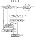
- FIG. 7 is a block diagram showing a constitution example of a timing analysis apparatus according to a second embodiment
- FIG. 8 is a flow chart showing an operation of the timing analysis apparatus in the second embodiment
- FIG. 9A , FIG. 9B and FIG. 9C are diagrams showing examples of tables of a coefficient of each number of stages
- FIG. 10 is a block diagram showing a constitution example of a computer capable of realizing the timing analysis apparatus.
- FIG. 11 is a diagram for explaining a problem of conventional static timing analysis.
- FIG. 11 is a schematic diagram for explaining a verification method of setup time in the conventional static timing analysis.
- reference numeral 111 denotes a source (source of supply) of a clock signal SCLK.
- the clock signal SCLK outputted from the source 111 is inputted into a clock input terminal ⁇ CLK> of a flip flop (FF) 116 via buffers 112 to 115 , and also inputted into a clock input terminal ⁇ CLK> of FF 118 .
- FF flip flop
- a data signal DAT is inputted into a data input terminal ⁇ DI> of the FF 116 .
- the data signal outputted from a data output terminal ⁇ DO> of the FF 116 in synchronism with the clock signal SCLK is inputted into a data input terminal ⁇ DI> of the FF 118 via a combinational circuit 117 .
- DS 1 to DS 8 show distributions of variations of respective elements (for convenience of explanation, the combinational circuit is also assumed to be an element) 113 to 117 , and 119 to 121 .
- the verification is conducted on the assumption that all the elements 112 to 117 on a data path 122 vary to a late side and all the elements 119 to 121 on a clock path 123 vary to an early side, as shown in FIG. 11 .
- the present invention is made in view of the above problem, and has its object to make it possible to carry out accurate timing analysis in consideration of variations in delay inside a chip according to the number of gate stages in a path.
- delay time which is considered when timing analysis in a path to be analyzed (target path) is executed
- 3 ⁇ ⁇ is a standard deviation of delay distribution
- the variation in delay which is considered when timing analysis is executed is optional, and it may be, for example, 4 ⁇ , 2 ⁇ , or ⁇ .
- FIGS. 1A and 1B are diagrams for explaining a change in delay distribution according to the number of circuit stages.
- reference numeral 11 denotes a starting point of a path (transmission path of a signal) which is a target of the timing analysis
- reference numeral 12 denotes an end of the path.
- the starting point 11 corresponds to a source (a supply source, an input terminal or the like) of a signal
- the end 12 corresponds to an input terminal of a flip flop.
- Reference symbol G(i) (i is a natural number) denotes a gate (element) such as a buffer which is connected in series between the starting point 11 and the end 12 .
- a central value (average value) of a delay of each gate G(i) is ⁇ i, and the variation (standard deviation) in the delay is ⁇ i.
- Reference symbol ⁇ (j) (j is a natural number) denotes a central value in a distribution of arrival time (delay) until a signal inputted from the starting point 11 arrives at the end 12 via the gates G( 1 ) to G(j) in the case in which the number of gate stages is j.
- Reference symbol ww(j) denotes a delay in the worst condition (in the case in which all the gates G(i) are delayed by 3 ⁇ ) which is obtained by the conventional method, and 3 ⁇ (j) is a delay when a 3 ⁇ delay occurs in view of the entire path, which are obtained according to the following expressions (1) and (2), respectively.
- ww(j) is the delay obtained by simply accumulating 3 ⁇ which is the delay in each gate G(i), while 3 ⁇ (j) is the delay in consideration of the probability according to the number of gate stages.
- FIG. 2 is a graph showing correlation between the number of circuit stages (number of gate stages) obtained by Monte Carlo analysis of the path delay and the delay in the entire path.
- the horizontal axis represents the number of circuit stages while the vertical axis represents the ratio to the accumulated delay.
- the ratio to the accumulated delay is the ratio of the delay value in consideration of the number of circuit stages of the entire path to the delay value of simple accumulation of 3 ⁇ of the variation of delay distribution in each gate on the path, and [3 ⁇ (j)]/[ww(j)].
- the ratio to the accumulated delay becomes smaller as the number of circuit stages becomes larger.
- the delay in the conventional method (accumulated delay) is “1” irrespective of the number of circuit stages, and therefore the difference 21 between the delay in consideration of the number of circuit stages shown by the solid line in FIG. 2 and “1”, namely, the difference between ww(j) and 3 ⁇ (j) is a timing margin excessively insured in the conventional timing verification. Namely, the timing margin excessively insured, which is shown by the difference between ww(j) and 3 ⁇ (j) becomes larger as the number of circuit stages is larger.
- timing analysis is performed with use of the delay distribution and its variation in the entire path in consideration of the probability according to the number of gate stages (3 ⁇ (j) corresponding to the number of gate stages in the aforementioned explanation).
- FIG. 3 is a block diagram showing a constitution example of a timing analysis apparatus according to a first embodiment of the present invention.
- reference numeral 32 denotes a circuit information input unit, in which circuit information 31 of a semiconductor integrated circuit which is the analysis target is inputted, and which outputs the circuit information to a coefficient arithmetically operating unit 33 and a timing analysis unit 37 .
- the circuit information 31 include, for example, a net list showing connection relationship among circuit elements and the like, library of the circuit elements and the like, delay information and the like.
- the coefficient arithmetically operating unit 33 cancels out a variation in delay in each gate in accordance with the number of gate stages in a path being an analysis target (target path) based on the inputted circuit information, and calculates a variation coefficient (OCV coefficient) in delay time in the target path according to the number of gate stages.
- the coefficient arithmetically operating unit 33 has a coefficient of the number of stages arithmetically operating section 34 , a variation width arithmetically operating section 35 and an OCV coefficient calculating section 36 .
- the coefficient of the number of stages arithmetically operating section 34 calculates the coefficient of the number of stages showing a variation amount of delay according to the number of gate stages in the target path by using the circuit information.
- the coefficient of the number of stages is the ratio of the delay in the entire path in consideration of the probability according to the number of gate stages and the delay obtained by simply accumulating the variation 3 ⁇ in each element existing on the path as in the prior art, and is calculated for each target path.
- the variation width arithmetically operating section 35 calculates variation width (variation amount) in a chip in the coefficient of the number of stages calculated in the coefficient of the number of stages arithmetically operating section 34 , namely, the variation width in the delay in the entire target path.
- the OCV coefficient calculating section 36 calculates the OCV coefficient in consideration of the number of gate stages with use of the circuit information, the coefficient of the number of stages calculated in the coefficient of the number of stages arithmetically operation section 34 , and the variation width calculated in the variation width calculating section 35 , and outputs the calculated OCV coefficient to the timing analysis unit 37 .
- the timing analysis unit 37 performs timing analysis (verification concerning the timing conditions relating to the setup time and hold time) of the target path with use of the circuit information and the OCV coefficient in consideration of the number of gate stages, and supplies the analysis result to a result output unit 38 .
- the result output unit 38 outputs the analysis result supplied by the timing analysis unit 37 by displaying it on a display device not shown, or outputting it as data, for example.
- FIG. 4 is a flow chart showing an operation of the timing analysis apparatus shown in FIG. 3 .
- the circuit information input unit 32 extracts a delay value (delay information) of each circuit element in the target path from the inputted circuit information 31 . Extraction of the delay value of each circuit element is performed for each of the data path and the clock path of the target path.
- this conventional OCV coefficient (in order to discriminate this from the OCV coefficient calculated in this embodiment, this conventional OCV coefficient will be called “old OCV coefficient”, hereinafter), which is used in the conventional method and the equal value irrespective of the number of gate stages, is included in the extracted delay value, the old OCV coefficient is deleted.
- the old OCV coefficient is deleted.
- step S 42 the coefficient arithmetically operating unit 33 executes the OCV coefficient calculation processing shown in FIG. 5 by using the circuit information including the delay value extracted in step S 41 , and calculates the OCV coefficient according to the number of gate stages of the target path.
- FIG. 5 is a flow chart showing an operation of the OCV coefficient calculation processing.
- the coefficient of the number of stages arithmetically operating unit 34 calculates the coefficient of the number of stages at the data path side of the target path based on the circuit information including the extracted delay value of each circuit element (step S 51 ).
- the coefficient of the number of stages is calculated for both of the case in which delay becomes large due to the variation in the delay distribution and the case in which the delay becomes small, namely for both of the worst condition and the best condition.
- the coefficient of the number of stages arithmetically operating unit 34 calculates the coefficient of the number of stages of the clock path side of the target path under the worst condition and the best condition by using the circuit information including the delay value of each circuit element (step S 52 ).
- the coefficient of the number of stages calculating unit 34 calculates the coefficient of the number of stages of the clock path side, after calculating the coefficient of the number of stages at the data path side of the target path, but the computation sequence of the coefficient of the number of stages of the data path side and the coefficient of the number of stages of the clock path side is optional.
- the variation width arithmetically operating section 35 estimates a calculation error in the delay calculation, based on the circuit information and the calculated coefficient of the number of stages (step S 53 ).
- the calculation error the errors under the worst condition and the best condition are estimated concerning the setup time and the hold time.
- the variation width arithmetically operating section 35 calculates variation width in the chip according to the number of gate stages under the worst condition and the best condition of the variation in the chip, based on the central value and the worst value under the worst condition and the central value and the best value under the best condition of the variation in the chip calculated based on the circuit information (step S 54 ).
- the variation width under the worst condition of the variation in the chip is calculated by calculating the difference between the worst value under the worst condition and its central value, and doubling the difference.
- the variation width in the chip is calculated for both the data path and the clock path of the target path.
- the OCV coefficient calculating section 36 calculates the OCV coefficient in consideration of the number of gate stages by using the coefficient of the number of stages, the calculation error of the delay calculation, and the variation width in the chip according to the number of gate stages, which are calculated in steps S 51 to S 54 as described above.
- the OCV coefficient the OCV coefficients under the worst condition and the best condition are calculated concerning the setup time and the hold time.
- the OCV coefficients under the worst condition and the best condition concerning the setup time, and the OCV coefficients under the worst condition and the best condition concerning the hold time, namely, the OCV coefficients respectively corresponding to the four different conditions are calculated, whereby the OCV coefficient calculation processing is finished.
- step S 43 the timing analysis unit 37 performs timing calculation relating to the setup time and the hold time in the target path by using the circuit information relating to the target path and the OCV coefficient calculated as described above, and supplies the calculation result to the result output unit 38 .
- the calculation result outputted from the timing analysis unit 37 to the result output unit 38 may be the calculation result itself obtained from the circuit information relating to the target path and the OCV coefficient, or the difference from the value obtained by the conventional method.
- FIG. 6A is a diagram showing an example of a circuit for explaining the OCV coefficient calculation processing.
- reference numeral 51 denotes a source (for example, a signal source or an input terminal) of a clock signal SCLK, and is a starting point of a path (target path) which is an analysis target.
- Reference numerals 52 , 53 , 54 and 55 are gates such as buffers, and are connected in series between the source 51 and a clock input terminal ⁇ CLK> of a flip flop (FF) 56 .
- FF flip flop
- a signal line for supplying a data signal DAT is connected to a data input terminal ⁇ DI> of the FF 56 .
- Reference numerals 57 and 58 denote gates, which are connected in series between a data output terminal ⁇ DO> of the FF 56 and a data input terminal ⁇ DA> of FF 59 . Namely, a data signal outputted from the FF 56 in synchronism with the clock signal SCLK is supplied to the FF 59 via the gates 57 and 58 .
- the FF 59 (precisely, the data input terminal ⁇ DA> of the FF 59 ) corresponds to the end of the target path.
- Reference numerals 60 , 61 and 62 denote gates, which are connected in series between the output terminal of the gate 52 and the clock input terminal ⁇ CK> of the FF 59 . In the following explanation, the FF is also assumed to be a gate.
- Reference numeral 66 denotes a synch clock path
- reference numeral 63 denotes a data path.
- the synch clock path 66 and the data path 63 respectively correspond to the clock path and data path in the aforementioned explanation.
- the data path 63 is constituted of a source clock path 64 (from the source 51 to the input of the FF 56 ), and an internal data path 65 (from the FF 56 to the input of the FF 59 ).
- FIG. 6B is a diagram for explaining the variation in the entire process and the variation in the chip.
- PV represents the variation in the entire process
- CVA represents the variation in the chip under the worst condition
- CVB represents the variation in the chip under the best condition.
- pm represents the central value in the distribution of the entire process.
- wm represents the central value and ww represents the worst value, under the worst condition in the variation in the chip.
- bm represents the central value and bb represents the best value, under the best condition in the variation in the chip (Note that the subscripts, wm, ww, bm and bb in the following explanation shall have the same meanings as in the aforementioned explanation.).
- step S 51 the coefficient of the number of stages Kn_max_DA in the worst condition and the coefficient of the number of stages Kn_min_DA in the best condition on the data path 63 side are calculated by using the following expressions (3) and (4).
- TgateCKD_ww ⁇ ocv_w + TlineCKD_ww ) + ⁇ ⁇ ( TgateDA_ww ⁇ ocv_w + TlineDA_ww ) ⁇ ⁇ Kn_max ⁇ _DA + ⁇ ⁇ ( TgateCKD_wdv 2 ) + ⁇ ⁇ ( TgateDA_wdv 2 ) ⁇ ⁇ ( TgateCKD_ww + TlineCKD_ww ) + ⁇ ⁇ ( TgateDA_ww + TlineDA_ww ) ⁇ ⁇ ( TgateDA_ww + TlineDA_ww ) ⁇ ⁇ TgateCKD_wdv + TgateCKD_ww - TgateCKD_wm ⁇ ⁇ TgateDA_wdv ⁇ _TgateDA ⁇ _ww - TgateDA_wm ( 3 )
- step S 52 the coefficient of the number of stages Kn_max_CK in the worst condition and the coefficient of the number of stages Kn_min_CK in the best condition on the synch clock path 66 side are calculated by using the following expressions (5) and (6).
- step S 53 the calculation errors Sw_error, Sb_error, Hw_error and Hb_error in the delay calculation are calculated by using the following expressions (7) to (10).
- Sw_error is the calculation error in the setup and the worst condition
- Sb_error is the calculation error in the setup and the best condition
- Hw_error is the calculation error in the hold and the worst condition
- Hb_error is the calculation error in the hold and the best condition.
- K 1 and K 2 are predetermined constants, and in the expressions (7) to (10), it is assumed that optional K 1 and K 2 can be set.
- Sw_error ⁇ ⁇ ⁇ ( TgateCKD_ww + TlineCKD_ww ) + ⁇ ⁇ ( TgateDA_ww + TlineDA_ww ) ⁇ ⁇ Kn_max ⁇ _DA ⁇ K ⁇ ⁇ 2 - ⁇ ⁇ ( TgateCK_ww + TlineCK_ww ) ⁇ Kn_max ⁇ _CK ⁇ K ⁇ ⁇ 1 ( 7 )
- Sb_error ⁇ ⁇ ⁇ ( TgateCKD_bb + TlineCKD_bb ) + ⁇ ⁇ ( TgateDA_bb + TlineDA_bb ) ⁇ ⁇ Kn_min ⁇ _DA ⁇ K ⁇ ⁇ 2 - ⁇ ⁇ ( TgateCK_bb + TlineCK_bb ) ⁇ Kn_min ⁇ _CK ⁇ K ⁇ ⁇ 1 ( 8 )
- Hw_error ⁇ ⁇ ( TgateCK_ww + TlineCK_w
- step S 54 variation widths OcvD_worst, OcvD_best, OcvC_worst, and OcvC_best in the chip according to the number of gate stages are calculated respectively by using the following expressions (11) to (14).
- OcvD_worst is the variation width under the worst condition in the data path 63
- OcvD_best is the variation width under the best condition in the data path 63
- OcvC_worst is the variation width under the worst condition in the synch clock path 66
- OcvC_best is the variation width under the best condition in the synch clock path 66 .
- ocv_w and ocv_b in the following expressions (11) and (12) are the same as ocv_w and ocv_b in the expressions (3) and (4), and ocv_w and ocv_b in the expressions (13) and (14) are the same as ocv_w and ocv_b in the expressions (5) and (6).
- OcvD_worst 2 ⁇ ⁇ ⁇ ⁇ ( TgateCKD_ww ⁇ ( 1 - ocv_w ) ) 2 ⁇ + ⁇ ⁇ ⁇ ( TgateDA_ww ⁇ ( 1 - ocv_w ) ) 2 ⁇ ( 11 )
- OcvD_best 2 ⁇ ⁇ ⁇ ⁇ ( TgateCKD_bb ⁇ ( ocv_b - 1 ) ) 2 ⁇ + ⁇ ⁇ ⁇ ( TgateDA_bb ⁇ ( ocv_b - 1 ) ) 2 ⁇ ( 12 )
- OcvD_worst 2 ⁇ ⁇ ⁇ ⁇ ( TgateCK_ww ⁇ ( 1 - ocv_w ) ) 2 ⁇ ( 13 )
- OcvD_best 2 ⁇ ⁇ ⁇ ⁇ ( TgateCK_bb ⁇ ( ocv_b - 1 ) ) 2
- step S 55 the OCV coefficients Sw_OCV, Sb_OCV, Hw_OCV, and Hb_OCV with consideration of the number of gate stages are calculated respectively according to the following expressions (15) to (18) by using the coefficients of the number of stages, the calculation errors of the delay calculation, the variation width in the variation in the chip and the like which are calculated as described above.
- Sw_OCV is the OCV coefficient in the setup and the worst condition
- Sb_OCV is the OCV coefficient in the setup and the best condition
- Hw_OCV is the OCV coefficient in the hold and the worst condition
- Hb_OCV is the OCV coefficient in the hold and the best condition.
- Sw_OCV Kn_max ⁇ _CK ⁇ ⁇ 1 + [ ( ⁇ ⁇ ( TgateCKD_ww + TlineCKD_ww ) + ⁇ ⁇ ( TgateDA_ww + TlineDA_ww ) ) ⁇ ( 1 - Kn_max ⁇ _DA ) - OcvC - error ] ⁇ ⁇ ( ⁇ ⁇ ( TgateCK_ww + TlineCK_ww ) ⁇ Kn_max ⁇ _CK ) ] ⁇ ( 15 )
- Sb_OCV Kn_min ⁇ _DA ⁇ ⁇ 1 - [ ( ⁇ ⁇ ( TgateCK_bb + TlineCK_bb ) ⁇ ( Kn_min ⁇ _CK - 1 ) - OcvD - error ] / [ ( ⁇ ⁇ ( TgateCKD_bb + TlineCKD_bb ) + ⁇ ⁇ ( TgateDA_bb + Tline
- Timing analysis is carried out by properly selecting the OCV coefficients Sw_OCV, Sb_OCV, Hw_OCV and Hb_OCV which are calculated as described above.
- the variation in the delay in each gate is cancelled out in accordance with the number of gate stages in the target path
- the OCV coefficients in the target path according to the number of gate stages are calculated by the coefficient arithmetically operating unit 33 , and timing analysis of the target path is performed in the timing analysis unit 37 by using the calculated OCV coefficients with the number of gate stages being considered.
- the variation degree in the entire path is reduced in accordance with the number of gate stages of the target path, and the excessive margin included in the conventional method can be eliminated. Accordingly, accurate timing analysis in consideration of the variation in the chip of a semiconductor integrated circuit can be carried out, and timing analysis according to the proper timing margin becomes possible. For example, constraints in timing is eased as compared with the prior art, and design of the semiconductor integrated circuit demanded of a high-speed operation can be made more easily than the prior art.
- a timing analysis apparatus which will be explained hereinafter, initially performs timing analysis with the conventional method, and carries out the same timing analysis as in the above-described first embodiment for only the path which is determined as violating the timing conditions based on the analysis result.
- FIG. 7 is a block diagram showing a constitution example of the timing analysis apparatus according to the second embodiment of the present invention.
- blocks having the same functions as the blocks shown in FIG. 3 are given the same reference numerals, and the redundant explanation will be omitted.
- reference numeral 71 denotes a timing analysis unit-A, which performs timing analysis of the target path by accumulating the variation in delay of each gate in the path which is an analysis target (target path).
- Reference numeral 72 denotes a determination unit, to which the analysis result of the timing analysis unit-A 71 is supplied, and which determines whether the target path satisfies previously specified timing conditions (conditions relating to the setup time and hold time). The determination unit 72 outputs the determination result to a result output unit 38 , and outputs the information relating to the path which does not satisfy the timing conditions to the coefficient arithmetically operating unit 33 .
- a timing analysis unit-B 37 constitutes a second timing analysis unit of the present invention
- the timing analysis unit-A 71 constitutes a first timing analysis unit of the present invention.
- FIG. 8 is a flow chart showing the operation of the timing analysis apparatus shown in FIG. 7 .
- step S 81 the circuit information input unit 32 extracts a delay value (delay information) of each circuit element for each of the data path and the clock path of the target path from the inputted circuit information 31 as in step S 41 shown in FIG. 4 .
- step S 82 the timing analysis unit-A 71 performs timing analysis of the target path by accumulating the variation in delay of each gate in the target path with the same method as the prior art by using the circuit information including the delay values extracted in step S 81 . Then, it extracts a Slack value (value of the timing margin) of the target path.
- step S 83 the determination unit 72 determines whether the timing conditions are violated (whether the previously specified timing conditions are satisfied or not) based on the Slack value obtained in step S 82 .
- the determination unit 72 supplies the analysis result to the result output unit 38 .
- the determination unit 72 outputs the information relating to the target path (the information which enables the target path to be discriminated) to the coefficient arithmetically operating unit 33 .
- step S 84 when the coefficient arithmetically operating unit 33 receives the information relating to the target path violating the timing conditions, which is outputted from the determination unit 72 , it executes the OCV coefficient calculation processing as in the first embodiment, and calculates the OCV coefficients according to the number of gate stages of the target path.
- the timing analysis unit-B 37 performs timing calculation relating to the setup time and the hold time in the target path by using the circuit information according to the target path and the calculated OCV coefficients (step S 85 ), and supplies the calculation result to the result output unit 38 (step S 86 ).
- the aforementioned processing is repeatedly executed for the other paths which are the analysis targets to finish the operation.
- timing analysis of the target path is performed in the timing analysis unit-A 71 by accumulating the variation in the delay time of each gate by using the circuit information 31 as in the prior art, and as a result, only when it is determined that the timing conditions previously specified are not satisfied in the determination unit 72 , timing analysis using the OCV coefficients with the number of gate stages being considered is performed as in the aforementioned first embodiment.
- timing analysis with the variation degree in the entire path being reduced according to the number of gate stages can be carried out by extracting only the paths with the rigid timing constraints.
- timing analysis units which are the timing analysis unit-A 71 and the timing analysis unit-B 37 are provided, but only one timing analysis unit may be provided and the circuit information, the OCV coefficient and the like to be inputted may be properly switched.
- the coefficient of the number of stages arithmetically operating section 34 in the coefficient arithmetically operating unit 33 calculates the coefficient of the number of stages each time based on the inputted circuit information 31 , but the tables of the coefficient of the number of stages showing the corresponding relationship of the number of gate stages and the coefficient of the number of stages in the clock path and the data path as shown in FIG. 9A to FIG. 9C may be created, and the coefficients of the number of stages may be obtained with reference to these tables of the coefficient of the number of stages.
- FIG. 9A is a table of the coefficient of the number of stages of the clock path.
- FIG. 9B is a table of the coefficient of the number of stages of the data path under the worst condition
- FIG. 9C is a table of the coefficient of the number of stages of the data path under the best condition.
- the coefficient of the number of stages arithmetically operating section 34 does not need to calculate the coefficient of the number of stages at each time based on the inputted circuit information 31 , thus making it possible to reduce the amount of the arithmetic operation processing and shorten the time required for timing analysis.
- the wiring between the gates has a constant value without considering the distribution of delay, but the distribution of delay may be considered, and in this case, arithmetic operation may be performed similarly to the gate.
- the timing analysis apparatuses in the aforementioned first and second embodiments can be constituted of a CPU or MPU of a computer, RAM, ROM, and the like, and can be realized by the operation of the program stored in the ROM, and the above-described program is included in the embodiments of the present invention.
- the timing analysis apparatus can be realized by recording the program for operating the computer to perform the above-described function in a recording medium such as, for example, a CD-ROM and making the computer read the program, and the recording medium in which the above-described program is recorded is included in the embodiments of the present invention.
- a recording medium for recording the above-described program a flexible disc, a hard disc, a magnetic tape, a magneto-optical disc, a nonvolatile memory card, and the like may be used other than a CD-ROM.
- a program product by which the function of the above-described embodiments is realized by the computer executing the program and performing the processing is included in the embodiments of the present invention.
- the above-described program product there are the program itself which realizes the function of the above-described embodiments, a computer in which the above-described program is read, a transmission apparatus capable of providing the above-described program to the computers communicably connected via a network, a network system including the transmission apparatus, and the like.
- the timing analysis apparatuses shown in the first and second embodiments each have a computer function 90 as shown in FIG. 10 , and each of the operations in the above-described embodiments is carried out by a CPU 91 thereof.
- the computer function 90 has a constitution in which the CPU 91 , a ROM 92 , a RAM 93 , a keyboard controller (KBC) 95 of a key board (KB) 99 , a CRT controller (CRTC) 96 of a CRT display (CRT) 100 as a display unit, a disc controller (DKC) 97 of a hard disc (HD) 101 and a flexible disc (FD) 102 , and a network interface card (NIC) 98 are connected communicably with each other via a system bus 94 .
- KBC keyboard controller
- CRTC CRT controller
- CRT CRT display
- DKC disc controller
- HD hard disc
- FD flexible disc
- NIC network interface card
- the CPU 91 generally controls each component connected to the system bus 94 by executing a software (program) stored in the ROM 92 or HD 101 , or a software (program) supplied from the FD 102 .
- the CPU 91 reads out the processing program for performing the operation as described above from the ROM 92 , the HD 101 , or the FD 102 and executes it, and thereby carries out the control to realize the operations in the above-described embodiments.
- the RAM 93 functions as a main memory, a work area or the like of the CPU 91 .
- the KBC 95 controls input of the instruction from the KB 99 , the pointing device not shown or the like.
- the CRTC 96 controls the display of the CRT 100 .
- the DKC 97 controls the access with the HD 101 and the FD 102 which stores a boot program, various kinds of applications, user files, a network management program, the above-described processing program and the like in the above-described embodiments.
- the NIC 98 exchanges date with the other devices on the network 103 bidirectionally.
- timing analysis according to proper timing margin becomes possible, for example, design of a semiconductor integrated circuit demanded of a high-speed operation can be made more easily than the prior art.
Landscapes
- Engineering & Computer Science (AREA)
- Computer Hardware Design (AREA)
- Physics & Mathematics (AREA)
- Theoretical Computer Science (AREA)
- Evolutionary Computation (AREA)
- Geometry (AREA)
- General Engineering & Computer Science (AREA)
- General Physics & Mathematics (AREA)
- Design And Manufacture Of Integrated Circuits (AREA)
Abstract
Description
Cycle_Time+Clock_path_time×ocv_worst−Data_time−Setup_time>0 (19)
Data_path_time×ocv_worst−Clock_path_time−Hold_time>0 (20)
Cycle_Time+Clock_path_time−Data_path_time×ocv_best−Setup_time>0 (21)
Data_path_time−Clock_path_time×ocv_best−Hold_time>0 (22)
Claims (13)
Applications Claiming Priority (2)
| Application Number | Priority Date | Filing Date | Title |
|---|---|---|---|
| JP2003-353950 | 2003-10-14 | ||
| JP2003353950A JP2005122298A (en) | 2003-10-14 | 2003-10-14 | Timing analysis apparatus, timing analysis method, and program |
Publications (2)
| Publication Number | Publication Date |
|---|---|
| US20050081171A1 US20050081171A1 (en) | 2005-04-14 |
| US7219320B2 true US7219320B2 (en) | 2007-05-15 |
Family
ID=34419932
Family Applications (1)
| Application Number | Title | Priority Date | Filing Date |
|---|---|---|---|
| US10/807,286 Expired - Fee Related US7219320B2 (en) | 2003-10-14 | 2004-03-24 | Semiconductor integrated circuit timing analysis apparatus timing analysis method and timing analysis program |
Country Status (2)
| Country | Link |
|---|---|
| US (1) | US7219320B2 (en) |
| JP (1) | JP2005122298A (en) |
Cited By (7)
| Publication number | Priority date | Publication date | Assignee | Title |
|---|---|---|---|---|
| US20060195807A1 (en) * | 2004-04-29 | 2006-08-31 | International Business Machines Corporation | Method and system for evaluating timing in an integated circuit |
| US20060225014A1 (en) * | 2005-03-29 | 2006-10-05 | Fujitsu Limited | Timing analysis method, timing analysis program, and timing analysis tool |
| US20070089076A1 (en) * | 2005-10-14 | 2007-04-19 | Sun Microsystems, Inc. | Application of consistent cycle context for related setup and hold tests for static timing analysis |
| US20070226668A1 (en) * | 2006-03-22 | 2007-09-27 | Synopsys, Inc. | Characterizing sequential cells using interdependent setup and hold times, and utilizing the sequential cell characterizations in static timing analysis |
| US20080104562A1 (en) * | 2006-10-31 | 2008-05-01 | Fujitsu Limited | Method and program for designing semiconductor integrated circuit |
| US8839178B1 (en) * | 2013-03-14 | 2014-09-16 | Medtronic, Inc. | Tool for evaluating clock tree timing and clocked component selection |
| US9660626B2 (en) | 2013-03-14 | 2017-05-23 | Medtronic, Inc. | Implantable medical device having clock tree network with reduced power consumption |
Families Citing this family (13)
| Publication number | Priority date | Publication date | Assignee | Title |
|---|---|---|---|---|
| JP2005352787A (en) * | 2004-06-10 | 2005-12-22 | Matsushita Electric Ind Co Ltd | Timing analysis method and timing analysis apparatus |
| JP4361838B2 (en) * | 2004-06-11 | 2009-11-11 | 富士通マイクロエレクトロニクス株式会社 | LSI design method |
| JP2006154951A (en) * | 2004-11-25 | 2006-06-15 | Fujitsu Ltd | Verification method and verification apparatus |
| US7685333B2 (en) * | 2005-03-22 | 2010-03-23 | Sigmatel, Inc | Method and system for communicating with memory devices utilizing selected timing parameters from a timing table |
| JP2006268479A (en) * | 2005-03-24 | 2006-10-05 | Fujitsu Ltd | Design support apparatus, design support method, design support program, and recording medium |
| JP4528659B2 (en) * | 2005-03-30 | 2010-08-18 | パナソニック株式会社 | Clock jitter calculation device, clock jitter calculation method, and clock jitter calculation program |
| JP4761906B2 (en) | 2005-09-27 | 2011-08-31 | ルネサスエレクトロニクス株式会社 | Semiconductor integrated circuit design method |
| JP4664231B2 (en) * | 2006-05-12 | 2011-04-06 | 富士通セミコンダクター株式会社 | Timing analysis method and timing analysis apparatus |
| JP4437824B2 (en) | 2007-02-13 | 2010-03-24 | 富士通株式会社 | Delay analysis result display program |
| JP5298946B2 (en) | 2009-02-25 | 2013-09-25 | 富士通セミコンダクター株式会社 | Design support program, design support apparatus, and design support method |
| US8117575B2 (en) | 2009-08-10 | 2012-02-14 | Taiwan Semiconductor Manufacturing Co., Ltd. | System and method for on-chip-variation analysis |
| US8584065B2 (en) * | 2011-05-05 | 2013-11-12 | Advanced Micro Devices, Inc. | Method and apparatus for designing an integrated circuit |
| JP2014021573A (en) | 2012-07-13 | 2014-02-03 | International Business Maschines Corporation | Method for optimizing netlist used in logic circuit design for semiconductor integrated circuit; device for assisting in logic circuit design using the same method; and computer program that can be executed on the same |
Citations (8)
| Publication number | Priority date | Publication date | Assignee | Title |
|---|---|---|---|---|
| US5365463A (en) * | 1990-12-21 | 1994-11-15 | International Business Machines Corporation | Method for evaluating the timing of digital machines with statistical variability in their delays |
| US5579510A (en) * | 1993-07-21 | 1996-11-26 | Synopsys, Inc. | Method and structure for use in static timing verification of synchronous circuits |
| US5917350A (en) * | 1997-03-28 | 1999-06-29 | Cypress Semiconductor Corp. | Asynchronous pulse discriminating synchronizing clock pulse generator with synchronous clock suspension capability for logic derived clock signals for a programmable device |
| JP3005888B2 (en) * | 1995-08-30 | 2000-02-07 | 株式会社岡村製作所 | Escalator shopping cart |
| JP2001306647A (en) * | 2000-04-21 | 2001-11-02 | Matsushita Electric Ind Co Ltd | Timing verification method |
| US6359479B1 (en) * | 1998-08-04 | 2002-03-19 | Juniper Networks, Inc. | Synchronizing data transfers between two distinct clock domains |
| US6473890B1 (en) * | 1999-09-20 | 2002-10-29 | Takuya Yasui | Clock circuit and method of designing the same |
| US20040254776A1 (en) * | 2002-01-11 | 2004-12-16 | Fujitsu Limited | Method for calculating delay time of semiconductor integrated circuit and delay time calculation system |
-
2003
- 2003-10-14 JP JP2003353950A patent/JP2005122298A/en active Pending
-
2004
- 2004-03-24 US US10/807,286 patent/US7219320B2/en not_active Expired - Fee Related
Patent Citations (8)
| Publication number | Priority date | Publication date | Assignee | Title |
|---|---|---|---|---|
| US5365463A (en) * | 1990-12-21 | 1994-11-15 | International Business Machines Corporation | Method for evaluating the timing of digital machines with statistical variability in their delays |
| US5579510A (en) * | 1993-07-21 | 1996-11-26 | Synopsys, Inc. | Method and structure for use in static timing verification of synchronous circuits |
| JP3005888B2 (en) * | 1995-08-30 | 2000-02-07 | 株式会社岡村製作所 | Escalator shopping cart |
| US5917350A (en) * | 1997-03-28 | 1999-06-29 | Cypress Semiconductor Corp. | Asynchronous pulse discriminating synchronizing clock pulse generator with synchronous clock suspension capability for logic derived clock signals for a programmable device |
| US6359479B1 (en) * | 1998-08-04 | 2002-03-19 | Juniper Networks, Inc. | Synchronizing data transfers between two distinct clock domains |
| US6473890B1 (en) * | 1999-09-20 | 2002-10-29 | Takuya Yasui | Clock circuit and method of designing the same |
| JP2001306647A (en) * | 2000-04-21 | 2001-11-02 | Matsushita Electric Ind Co Ltd | Timing verification method |
| US20040254776A1 (en) * | 2002-01-11 | 2004-12-16 | Fujitsu Limited | Method for calculating delay time of semiconductor integrated circuit and delay time calculation system |
Non-Patent Citations (3)
| Title |
|---|
| Hasegawa et al., "Timing Analysis System Heart for Large Scale Circuit (1) Procedure for Increasing Speed," 35<SUP>th </SUP>National Convention, Lecture Symposium (III), 1987, 5 pages. * |
| Patent Abstracts of Japan of JP 2002222232 A dated Aug. 9, 2002. |
| Patent Abstracts of Japan of JP 63098042 A dated Apr. 28, 1988. |
Cited By (15)
| Publication number | Priority date | Publication date | Assignee | Title |
|---|---|---|---|---|
| US20080313590A1 (en) * | 2004-04-29 | 2008-12-18 | International Business Machines Corporation | Method and system for evaluating timing in an integrated circuit |
| US20060195807A1 (en) * | 2004-04-29 | 2006-08-31 | International Business Machines Corporation | Method and system for evaluating timing in an integated circuit |
| US7962874B2 (en) | 2004-04-29 | 2011-06-14 | International Business Machines Corporation | Method and system for evaluating timing in an integrated circuit |
| US7444608B2 (en) * | 2004-04-29 | 2008-10-28 | International Business Machines Corporation | Method and system for evaluating timing in an integrated circuit |
| US20060225014A1 (en) * | 2005-03-29 | 2006-10-05 | Fujitsu Limited | Timing analysis method, timing analysis program, and timing analysis tool |
| US7669154B2 (en) * | 2005-03-29 | 2010-02-23 | Fujitsu Microelectronics Limited | Timing analysis method, timing analysis program, and timing analysis tool |
| US20070089076A1 (en) * | 2005-10-14 | 2007-04-19 | Sun Microsystems, Inc. | Application of consistent cycle context for related setup and hold tests for static timing analysis |
| US20070226668A1 (en) * | 2006-03-22 | 2007-09-27 | Synopsys, Inc. | Characterizing sequential cells using interdependent setup and hold times, and utilizing the sequential cell characterizations in static timing analysis |
| US7506293B2 (en) * | 2006-03-22 | 2009-03-17 | Synopsys, Inc. | Characterizing sequential cells using interdependent setup and hold times, and utilizing the sequential cell characterizations in static timing analysis |
| US20080295053A1 (en) * | 2006-03-22 | 2008-11-27 | Synopsys, Inc. | Characterizing Sequential Cells Using Interdependent Setup And Hold Times, And Utilizing The Sequential Cell Characterizations In Static Timing Analysis |
| US7774731B2 (en) | 2006-03-22 | 2010-08-10 | Synopsys, Inc. | Characterizing sequential cells using interdependent setup and hold times, and utilizing the sequential cell characterizations in static timing analysis |
| US7930665B2 (en) * | 2006-10-31 | 2011-04-19 | Fujitsu Semiconductor Limited | Method and program for designing semiconductor integrated circuit |
| US20080104562A1 (en) * | 2006-10-31 | 2008-05-01 | Fujitsu Limited | Method and program for designing semiconductor integrated circuit |
| US8839178B1 (en) * | 2013-03-14 | 2014-09-16 | Medtronic, Inc. | Tool for evaluating clock tree timing and clocked component selection |
| US9660626B2 (en) | 2013-03-14 | 2017-05-23 | Medtronic, Inc. | Implantable medical device having clock tree network with reduced power consumption |
Also Published As
| Publication number | Publication date |
|---|---|
| JP2005122298A (en) | 2005-05-12 |
| US20050081171A1 (en) | 2005-04-14 |
Similar Documents
| Publication | Publication Date | Title |
|---|---|---|
| US7219320B2 (en) | Semiconductor integrated circuit timing analysis apparatus timing analysis method and timing analysis program | |
| US7428716B2 (en) | System and method for statistical timing analysis of digital circuits | |
| US7555740B2 (en) | Method and system for evaluating statistical sensitivity credit in path-based hybrid multi-corner static timing analysis | |
| US7117466B2 (en) | System and method for correlated process pessimism removal for static timing analysis | |
| US8645888B2 (en) | Circuit timing analysis incorporating the effects of temperature inversion | |
| US20080034338A1 (en) | Timing analysis method and device | |
| US8056038B2 (en) | Method for efficiently checkpointing and restarting static timing analysis of an integrated circuit chip | |
| US6718523B2 (en) | Reduced pessimism clock gating tests for a timing analysis tool | |
| US20050223344A1 (en) | Power-consumption calculation method and apparatus | |
| US10740520B2 (en) | Pessimism in static timing analysis | |
| US6412101B1 (en) | Simultaneous path optimization (SPO) system and method | |
| US20110296361A1 (en) | Circuit analysis method | |
| Onaissi et al. | A linear-time approach for static timing analysis covering all process corners | |
| US6871329B2 (en) | Design system of integrated circuit and its design method and program | |
| US8302049B2 (en) | Method for enabling multiple incompatible or costly timing environment for efficient timing closure | |
| US7562266B2 (en) | Method and device for verifying timing in a semiconductor integrated circuit | |
| JP4053969B2 (en) | Semiconductor integrated circuit design apparatus and semiconductor integrated circuit design method | |
| US10372851B2 (en) | Independently projecting a canonical clock | |
| US10055532B2 (en) | Collapsing terms in statistical static timing analysis | |
| US9405871B1 (en) | Determination of path delays in circuit designs | |
| US7448006B2 (en) | Logic-synthesis method and logic synthesizer | |
| JP3561661B2 (en) | Semiconductor integrated circuit and method of designing semiconductor integrated circuit |
Legal Events
| Date | Code | Title | Description |
|---|---|---|---|
| AS | Assignment |
Owner name: FUJITSU LIMITED, JAPAN Free format text: ASSIGNMENT OF ASSIGNORS INTEREST;ASSIGNORS:KAWANO, TETSUO;YOSHIKAWA, SATORU;HOSONO, TOSHIKATSU;AND OTHERS;REEL/FRAME:015135/0212 Effective date: 20040218 |
|
| CC | Certificate of correction | ||
| FEPP | Fee payment procedure |
Free format text: PAYOR NUMBER ASSIGNED (ORIGINAL EVENT CODE: ASPN); ENTITY STATUS OF PATENT OWNER: LARGE ENTITY |
|
| AS | Assignment |
Owner name: FUJITSU MICROELECTRONICS LIMITED, JAPAN Free format text: ASSIGNMENT OF ASSIGNORS INTEREST;ASSIGNOR:FUJITSU LIMITED;REEL/FRAME:021985/0715 Effective date: 20081104 Owner name: FUJITSU MICROELECTRONICS LIMITED,JAPAN Free format text: ASSIGNMENT OF ASSIGNORS INTEREST;ASSIGNOR:FUJITSU LIMITED;REEL/FRAME:021985/0715 Effective date: 20081104 |
|
| REMI | Maintenance fee reminder mailed | ||
| LAPS | Lapse for failure to pay maintenance fees | ||
| STCH | Information on status: patent discontinuation |
Free format text: PATENT EXPIRED DUE TO NONPAYMENT OF MAINTENANCE FEES UNDER 37 CFR 1.362 |
|
| FP | Lapsed due to failure to pay maintenance fee |
Effective date: 20110515 |