US7190148B2 - Overcharge/overdischarge detection apparatus, overcharge/overdischarge detection circuit, and semiconductor apparatus - Google Patents
Overcharge/overdischarge detection apparatus, overcharge/overdischarge detection circuit, and semiconductor apparatus Download PDFInfo
- Publication number
- US7190148B2 US7190148B2 US11/069,201 US6920105A US7190148B2 US 7190148 B2 US7190148 B2 US 7190148B2 US 6920105 A US6920105 A US 6920105A US 7190148 B2 US7190148 B2 US 7190148B2
- Authority
- US
- United States
- Prior art keywords
- terminal
- detection
- secondary battery
- overcharge
- circuit
- Prior art date
- Legal status (The legal status is an assumption and is not a legal conclusion. Google has not performed a legal analysis and makes no representation as to the accuracy of the status listed.)
- Expired - Fee Related
Links
Images


Classifications
-
- H—ELECTRICITY
- H01—ELECTRIC ELEMENTS
- H01M—PROCESSES OR MEANS, e.g. BATTERIES, FOR THE DIRECT CONVERSION OF CHEMICAL ENERGY INTO ELECTRICAL ENERGY
- H01M10/00—Secondary cells; Manufacture thereof
- H01M10/42—Methods or arrangements for servicing or maintenance of secondary cells or secondary half-cells
-
- H—ELECTRICITY
- H02—GENERATION; CONVERSION OR DISTRIBUTION OF ELECTRIC POWER
- H02G—INSTALLATION OF ELECTRIC CABLES OR LINES, OR OF COMBINED OPTICAL AND ELECTRIC CABLES OR LINES
- H02G15/00—Cable fittings
- H02G15/007—Devices for relieving mechanical stress
-
- H02J7/61—
-
- H02J7/62—
-
- H02J7/63—
-
- H02J7/663—
-
- Y—GENERAL TAGGING OF NEW TECHNOLOGICAL DEVELOPMENTS; GENERAL TAGGING OF CROSS-SECTIONAL TECHNOLOGIES SPANNING OVER SEVERAL SECTIONS OF THE IPC; TECHNICAL SUBJECTS COVERED BY FORMER USPC CROSS-REFERENCE ART COLLECTIONS [XRACs] AND DIGESTS
- Y02—TECHNOLOGIES OR APPLICATIONS FOR MITIGATION OR ADAPTATION AGAINST CLIMATE CHANGE
- Y02E—REDUCTION OF GREENHOUSE GAS [GHG] EMISSIONS, RELATED TO ENERGY GENERATION, TRANSMISSION OR DISTRIBUTION
- Y02E60/00—Enabling technologies; Technologies with a potential or indirect contribution to GHG emissions mitigation
- Y02E60/10—Energy storage using batteries
Definitions
- the present invention generally relates to an overcharge/overdischarge detection apparatus, an overcharge/overdischarge detection circuit, and a semiconductor apparatus, and more particularly to a overcharge/overdischarge detection apparatus, overcharge/overdischarge detection circuit, and a semiconductor apparatus for controlling charge/discharge of a secondary battery
- a battery pack using lithium-ion batteries is mounted as a power source for mobile devices, for example, mobile phones.
- the lithium-ion battery has its life-span excessively shortened when subjected to, for example, overcharge, overdischarge, overcurrent, and/or short circuiting.
- a protection circuit is mounted thereto (See Japanese Laid-Open Patent Application No. 2003-59467)
- the conventional battery pack is not provided with a function of detecting leakage of the battery. Therefore, in a case where the battery has a leakage (e.g. electrolyte leakage), the battery is continued to be used without noticing the leakage. Such progression of leakage may lead to problems, for example, an apparatus main body being adversely affected by leaking electrolyte.
- a leakage e.g. electrolyte leakage
- an object of the present invention to provide an overcharge/overdischarge detection apparatus, an overcharge/overdischarge detection circuit, and a semiconductor apparatus for achieving reliable detection of leakage with a simple configuration.
- the invention provides an overcharge/overdischarge detection apparatus including: a detection terminal being in an open state; a detection part for detecting application of voltage to the detection terminal; a switch part for switchably connecting and disconnecting a secondary battery with an external circuit; and a control part for controlling the switch part in a case where the detection part detects the application of voltage to the detection terminal.
- control part may include an abnormality detection part for detecting an abnormality in the secondary battery and outputting an abnormality signal, and a logic circuit for switching off the switch part when receiving the abnormality signal from the abnormality detection part, wherein the abnormality signal are controlled for switching off the switch part.
- the detection terminal may include a test terminal for testing operation of the control part in accordance with an external signal, wherein the test terminal is connected to the control part.
- the present invention provides an overcharge/overdischarge detection circuit including: a detection terminal being in an open state; a detection circuit for detecting application of voltage to the detection terminal; a switch part for switchably connecting and disconnecting a secondary battery with an external circuit; and a control part for controlling the switch part in a case where the detection circuit detects the application of voltage to the detection terminal.
- control part may include an abnormality detection circuit for detecting an abnormality in the secondary battery and outputting an abnormality signal, and a logic circuit for switching off the switch part when receiving the abnormality signal from the abnormality detection circuit, wherein the abnormality signal are controlled for switching off the switch part.
- the detection terminal may include a test terminal for testing operation of the control part in accordance with an external signal, wherein the test terminal is connected to the control part.
- the present invention provides a semiconductor apparatus including: a detection terminal being in an open state; a detection circuit for detecting application of voltage to the detection terminal; a switch part for switchably connecting and disconnecting a secondary battery with an external circuit; and a control part for controlling the switch part in a case where the detection circuit detects the application of voltage to the detection terminal.
- control part may include an abnormality detection circuit for detecting an abnormality in the secondary battery and outputting an abnormality signal, and a logic circuit for switching off the switch part when receiving the abnormality signal from the abnormality detection circuit, wherein the abnormality signal are controlled for switching off the switch part.
- the detection terminal may include a test terminal for testing operation of the control part in accordance with an external signal, wherein the test terminal is connected to the control part.
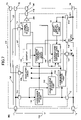
- FIG. 1 is a circuit diagram showing an exemplary configuration of a battery pack according to a first embodiment of the present invention
- FIG. 2 is an exploded perspective drawing of a battery pack according to a first embodiment of the present invention
- FIG. 3A is a top perspective view of a circuit board according to an embodiment of the present invention.
- FIG. 3B is a bottom perspective view of a circuit board according to an embodiment of the present invention.
- FIG. 4 is a block diagram showing a modified example of a leakage detection part according to an embodiment of the present invention.
- FIG. 5 is a diagram for explaining an operation of a modified example of a leakage detection part according to an embodiment of the present invention.
- FIG. 6 is a circuit diagram showing an exemplary configuration of a battery pack according to a second embodiment of the present invention.
- FIG. 7 is a circuit diagram showing an exemplary configuration of a battery pack according to a third embodiment of the present invention.
- FIG. 1 is a circuit diagram showing an exemplary configuration of a battery pack 100 according to a first embodiment of the present invention.
- FIG. 2 is an exploded perspective drawing of the battery pack 100 according to the first embodiment of the present invention.
- the battery pack 100 may be, for example, a storage battery used as a power source of a mobile device such as a mobile phone.
- the battery pack 100 includes, for example, a casing 111 , a cover 112 , a secondary battery 113 , and a circuit board 114 .
- the casing 111 and the cover 112 may be formed of, for example, resin material.
- the casing 111 and the cover 112 provide a housing part 120 for housing the secondary battery 113 and the circuit board 114 therein.
- the secondary battery 113 may be, for example, a lithium-ion battery.
- a metal plate (electrode plate) 121 which is welded to a terminal T 1 of the circuit board 114 , is soldered to a positive electrode of the secondary battery 113 .
- a metal plate 122 which is welded to a terminal T 2 of the circuit board 114 , is soldered to a negative electrode of the secondary battery 113 .
- FIG. 3A is a top perspective view of the circuit board 114 according to the first embodiment of the present invention
- FIG. 3B is a bottom perspective view of the circuit board 114 according to the first embodiment of the present invention.
- the circuit board 114 has an overcharge/overdischarge detection IC (Integrated Circuit) 131 , transistors M 11 , M 12 , and a resistance R 11 provided on a printed-wiring board 130 .
- the transistor M 11 is configured as an n channel MOS field effect transistor.
- the transistor M 11 having a gate connected to a terminal T 15 of the overcharge/overdischarge detection IC 131 , controls discharge when switched off.
- the transistor M 12 is configured as an n channel MOS field effect transistor.
- the transistor M 12 having a gate connected to a terminal T 16 of the overcharge/overdischarge detection IC 131 , also restricts discharge when switched off.
- the overcharge/overdischarge detection IC 131 includes an overcharge detection part 141 , an overdischarge detection part 142 , an overcurrent detection part 143 , a short circuit detection part 144 , a leakage detection part 145 , an oscillator circuit 146 , a counter 147 , an overcharge control logic circuit 148 , and an overdischarge control logic circuit 149 , as shown in FIG. 1 .
- the overcharge detection part 141 is connected between a terminal T 11 and a terminal T 12 and is supplied with voltage of both ends of the secondary battery 113 .
- the output of the overcharge detection part 141 is set as a high level when voltage of both ends of the secondary battery 113 is less than a predetermined overcharge voltage.
- the output of the overcharge detection part 141 is set as a low level when voltage of the secondary battery 113 is greater than the predetermined overcharge voltage (i.e. overcharge state of the secondary battery 113 ).
- the predetermined overcharge voltage is set beforehand in accordance with the characteristic(s) of the secondary battery 113 .
- the output of the overcharge detection part 141 is supplied to the oscillator circuit 146 and the overcharge control logic circuit 148 .
- the overdischarge detection part 142 is also connected between the terminal T 11 and the terminal T 12 and is supplied with voltage of both ends of the secondary battery 113 .
- the output of the overdischarge detection part 142 is set as a high level when voltage of both ends of the secondary battery 113 is greater than a predetermined overdischarge voltage.
- the output of the overdischarge detection part 142 is set as a low level when voltage of the secondary battery 113 is less than the predetermined overcharge voltage (i.e. overdischarge state of the secondary battery 113 ).
- the predetermined overdischarge voltage is set beforehand in accordance with the characteristic(s) of the secondary battery 113 .
- the output of the overdischarge detection part 142 is supplied to the oscillator circuit 146 and the overdischarge control logic circuit 149 .
- the overcurrent detection part 143 is connected to a terminal T 13 .
- the terminal T 13 is connected to a terminal T 4 via a resistance R 11 .
- the terminal T 4 is connected to a negative electrode of an external circuit (e.g. load).
- the output of overcurrent detection part 143 is set as a high level when voltage of the terminal T 13 is less than a predetermined overcurrent voltage.
- the output of the overcurrent detection part 143 is set as a low level when voltage of the terminal T 13 is greater than the predetermined overcurrent voltage (i.e. overcurrent state of the current supplied from the secondary battery 113 to the load).
- the predetermined overcurrent voltage is set beforehand in accordance with the characteristic(s) of the secondary battery 113 .
- the output of the overcurrent detection part 143 is supplied to the oscillator circuit 146 and the overdischarge control logic circuit 149 .
- the short circuit detection part 144 is connected to the terminal T 13 .
- the output of the short circuit detection part 144 is set as a high level when voltage of the terminal T 13 is less than a predetermined short circuit voltage.
- the output of the short circuit detection part 144 is set as a low level when voltage of the terminal T 13 is greater than the predetermined short circuit voltage (i.e. short circuited state of the secondary battery 113 ).
- the predetermined short circuit voltage is set beforehand in accordance with the characteristic(s) of the secondary battery 113 .
- the output of the short circuit detection part 144 is supplied to the overdischarge control logic circuit 149 .
- the leakage detection part 145 is connected to the terminal T 14 .
- the terminal T 14 is connected to a wiring pattern 132 formed on the printed-wiring board 130 .
- the wiring pattern 132 is extended from the terminal T 14 to the vicinity of the terminal T 1 .
- the wiring pattern 132 has one end (toward terminal T 14 ) soldered to the terminal T 14 and the other end (toward the vicinity of terminal T 1 ) provided in an open state.
- the leakage detection part 145 includes, for example, an inverting amplifier.
- the liquid detection part 145 which is input with a potential of the terminal T 14 , detects that the potential of the terminal T 14 has risen to VDD and sets its output to a low level.
- the output of the leakage detection part 145 is supplied to the overcharge control logic circuit 148 , the overdischarge control logic circuit 149 , and the oscillator circuit 146 .
- the oscillator circuit 146 starts oscillation and outputs a pulse(s).
- the oscillator circuit 146 is connected to a test terminal T 17 .
- the test terminal T 17 is a terminal used for control during an operation test of an internal circuit part(s), for example, by using an external signal after assembly, or shipment.
- the test terminal T 17 is connected to a test terminal T 5 via a wiring pattern 133 formed on the circuit board 114 .
- the control for testing the overcharge/overdischarge detection IC 131 is executed through the test terminal T 5 formed on the circuit board 114 .
- the pulse output from the oscillator circuit 146 is supplied to the counter 147 .
- the counter 147 counts the pulse output from the oscillator circuit 146 .
- the count number of the counter 147 is supplied to the overcharge control logic circuit 148 and the overdischarge control logic circuit 149 . It is to be noted that the counter is reset when the output of the overdischarge control logic circuit is switched from low level to high level.
- the outputs of the overcharge detection part 141 and the leakage detection part 145 and the count number of the counter 147 are supplied to the overcharge control logic circuit 148 .
- the output of the overcharge control logic circuit 148 is set to a low level in a case where the output of the overcharge detection part 141 and/or the leakage detection part 145 is a low level(s) and thus the count number of the counter 147 is a predetermined count number.
- the output of the overcharge control logic circuit 148 is set to a high level when outputs of the overcharge detection part 141 and the leakage detection part 145 and the count number of the counter 147 are in a state other than the foregoing case.
- the output of the overcharge control logic circuit 148 is supplied to a terminal T 16 .
- the terminal T 16 is connected to a gate of the transistor M 12 .
- the outputs of the overdischarge detection part 142 , the overcurrent detection part 143 , the short circuit detection part 144 , and the leakage detection part 145 , and the count number of the counter 147 are supplied to the overdischarge control logic circuit 149 .
- the output of the overdischarge control logic circuit 149 is a low level in a case where the output of the short circuit detection part 144 and/or the leakage detection part 145 is a low level and thus the count number of the counter 147 is a predetermined number.
- the output of the overdischarge control logic circuit 149 is set to a high level when outputs of the short circuit detection part 144 and/or the leakage detection part 145 and the count number of the counter 147 are in a state other than the foregoing case.
- the output of the overdischarge control logic circuit 149 is supplied to a terminal T 15 .
- the terminal T 15 is connected to a gate of the transistor M 11 .
- the transistor M 11 has its gate connected to the terminal T 15 , its source connected to a terminal T 2 , and its drain connected to a source of the transistor M 12 .
- the transistor M 12 has its gate connected to the terminal T 16 , its source connected to the drain of the transistor M 11 , and its drain connected to the terminal T 4 .
- the transistor M 11 is configured as an n channel MOS field effect transistor.
- the transistor M 11 is switched off when the output of the terminal T 15 is a low level, and is switched on when the output of the terminal T 16 is a high level.
- the transistor M 12 is also configured as an n channel MOS field effect transistor. The transistor M 12 is switched off when the output of the terminal T 16 is a low level, and is switched on when the output of the terminal T 16 is a high level.
- the secondary battery 113 and the terminal T 4 are disconnected. This causes the secondary battery 113 and the load to disconnect. Accordingly, current can be preventing from being applied to the load in a case of overcharge, overdischarge, overcurrent, short circuit, and/or leakage; thereby the secondary battery 113 can be protected.
- electrolyte leaks from a vicinity of the positive electrode of the secondary battery 113 .
- the leaking electrolyte travels across the electrode plate 121 until reaching to the terminal T 1 of the circuit board 114 .
- the electrolyte spreads in the circuit board 114 and causes a short circuit between the terminal T 1 (i.e. positive electrode of the secondary battery 113 ) and the wiring pattern 132 when situated between the terminal T 1 and the wiring pattern 132 .
- the terminal T 14 of the overcharge/overdischarge detection IC 131 becomes a high level.
- the output of the leakage detection part 145 becomes a low level.
- the inputs of the oscillator circuit 146 , the overcharge control logic circuit 148 , and the overdischarge control logic circuit 149 become low levels.
- the oscillator circuit 146 outputs a pulse when the output of the leakage detection part 145 becomes a low level.
- the counter 147 counts the pulse output from the oscillator circuit 146 .
- the outputs of the overcharge control logic circuit 148 and the overdischarge control logic circuit 149 become low levels when the count number of the counter 147 reaches the predetermined count number.
- the transistor M 12 is switched off.
- the overdischarge control logic circuit 149 becomes a low level, the transistor M 11 is switched off.
- a leakage e.g. electrolyte leakage
- the potential of the terminal T 14 rises.
- the secondary battery 113 is disconnected with an external circuit. Accordingly, progression of the leakage and adverse effects to the external circuit can be prevented.
- the leakage detection according to the first embodiment of the present invention can be achieved simply by adding the terminal T 14 and the leakage detection part 145 since the transistors M 11 and M 12 are switched by controlling signals input from, for example, the overcharge detection part 141 and the overdischarge detection part 142 to the overcharge control logic circuit 148 and the overdischarge control logic circuit 149 . Accordingly, only a minimal change is required for the configuration of the circuit according to the first embodiment of the present invention.
- FIG. 4 is a block diagram showing an exemplary modified leakage detection part 150 (i.e. modification of the leakage detection part 145 ) according to the first embodiment of the present invention
- FIG. 5 is a diagram for explaining an operation of the exemplary modified leakage detection part 150 according to the first embodiment of the present invention.
- FIG. 5(A) shows an input of an inverter 151
- FIG. 5(B) shows an output of the inverter 151
- FIG. 5(C) shows an output of a delay circuit 152 .
- the leakage detection part 150 includes the inverter 151 and the delay circuit 152 .
- the inverter 151 inverts and outputs an input from the terminal T 14 .
- the output of the inverter 151 is supplied to the delay circuit 152 .
- the delay circuit 152 delays the output from the inverter 151 for a predetermined delay period ⁇ t 0 , as shown in FIG. 5(C) .
- the output of the delay circuit 152 is supplied to the overcharge control logic circuit 148 and the overdischarge control logic circuit 149 .
- the modified leakage detection part 150 since the input from the terminal T 14 is output from the inverter 151 in delayed manner to the overcharge control logic circuit 148 and the overdischarge control logic circuit 149 , problems such as noise can be prevented. Accordingly, operation can be executed more steadily.
- FIG. 6 is a circuit diagram showing an exemplary configuration of a battery pack 200 according to a second embodiment of the present invention.
- like components are denoted with like numerals as of the first embodiment of the present invention shown in FIG. 1 , and are not further explained.
- the battery pack 200 includes a circuit board 214 which is configured differently from that of the first embodiment of the present invention.
- the test terminal T 17 of an overcharge/overdischarge detection IC 231 is configured to serve also as the terminal T 14 provided for leakage detection in the first embodiment of the present invention.
- the test terminal T 17 of the overcharge/overdischarge detection IC 231 is connected to the test terminal T 5 for connecting to the outside and is also connected to one end of the wiring pattern 132 . Furthermore, the test terminal T 17 is connected to the oscillator 146 and the leakage detection part 145 inside the overcharge/overdischarge detection IC 231 .
- FIG. 7 is a circuit diagram showing an exemplary configuration of a battery pack 300 according to a third embodiment of the present invention.
- the battery pack 300 includes a circuit board 314 which is configured differently from that of the first embodiment of the present invention.
- the circuit board 314 includes a leakage reporting terminal T 6 serving as a terminal for reporting a leakage.
- the terminal T 6 is connected to a higher level apparatus when the battery pack 300 is mounted on an apparatus.
- the leakage reporting terminal T 6 is connected to another leakage reporting terminal T 18 of an overcharge/overdischarge detection IC 331 via a wiring pattern 134 .
- the output of the leakage detection part 145 is connected to the leakage reporting terminal T 18 via a buffer 350 .
- a leakage detection signal obtained from the leakage detection part 145 can be output to an external circuit, to thereby report a leakage of the battery pack 300 . Therefore, the user can be informed of the cause for the cease of the power supply.
- an LED for example, may be employed for reporting the leakage of the battery pack 300 to the user.
Landscapes
- Engineering & Computer Science (AREA)
- Manufacturing & Machinery (AREA)
- Chemical & Material Sciences (AREA)
- Chemical Kinetics & Catalysis (AREA)
- Electrochemistry (AREA)
- General Chemical & Material Sciences (AREA)
- Charge And Discharge Circuits For Batteries Or The Like (AREA)
- Secondary Cells (AREA)
- Tests Of Electric Status Of Batteries (AREA)
Abstract
Description
Claims (9)
Applications Claiming Priority (2)
| Application Number | Priority Date | Filing Date | Title |
|---|---|---|---|
| JP2004-284855 | 2004-09-29 | ||
| JP2004284855A JP2006101635A (en) | 2004-09-29 | 2004-09-29 | Over-charge/discharge detection device, and over-charge/discharge detection circuit and semiconductor device |
Publications (2)
| Publication Number | Publication Date |
|---|---|
| US20060076930A1 US20060076930A1 (en) | 2006-04-13 |
| US7190148B2 true US7190148B2 (en) | 2007-03-13 |
Family
ID=36144601
Family Applications (1)
| Application Number | Title | Priority Date | Filing Date |
|---|---|---|---|
| US11/069,201 Expired - Fee Related US7190148B2 (en) | 2004-09-29 | 2005-02-28 | Overcharge/overdischarge detection apparatus, overcharge/overdischarge detection circuit, and semiconductor apparatus |
Country Status (4)
| Country | Link |
|---|---|
| US (1) | US7190148B2 (en) |
| JP (1) | JP2006101635A (en) |
| KR (1) | KR20060043132A (en) |
| CN (1) | CN1755385A (en) |
Cited By (7)
| Publication number | Priority date | Publication date | Assignee | Title |
|---|---|---|---|---|
| US20080278116A1 (en) * | 2007-05-08 | 2008-11-13 | Fuji Electric Device Technology Co., Ltd | Battery protective device and semiconductor integrated circuit device |
| US20100295550A1 (en) * | 2009-02-20 | 2010-11-25 | National Semiconductor Corporation | Adaptive energy management terminal for a battery |
| US20120062033A1 (en) * | 2010-09-09 | 2012-03-15 | Toshiba Tec Kabushiki Kaisha | Power supply circuit using rechargeable battery |
| US20210263104A1 (en) * | 2020-02-24 | 2021-08-26 | Ford Global Technologies, Llc | Vehicle traction battery over-discharge diagnosing method and assembly |
| US11249143B2 (en) * | 2017-11-14 | 2022-02-15 | Huawei Technologies Co., Ltd. | Charging apparatus and charging system |
| US20230246470A1 (en) * | 2022-01-31 | 2023-08-03 | Google Llc | Battery Zero-Voltage Detection Methodologies and Applications Thereof |
| US12431546B2 (en) | 2022-07-01 | 2025-09-30 | Apple Inc. | Detecting electrolyte on circuit boards |
Families Citing this family (20)
| Publication number | Priority date | Publication date | Assignee | Title |
|---|---|---|---|---|
| KR100943594B1 (en) * | 2006-03-27 | 2010-02-24 | 삼성에스디아이 주식회사 | Protection circuit module and battery pack using same |
| JP4626578B2 (en) * | 2006-06-27 | 2011-02-09 | ソニー株式会社 | Battery pack |
| JP2008151526A (en) * | 2006-12-14 | 2008-07-03 | Matsushita Electric Ind Co Ltd | Secondary battery deterioration judgment device and backup power source |
| KR100938080B1 (en) * | 2007-09-28 | 2010-01-21 | 삼성에스디아이 주식회사 | Safety circuit and battery pack using same |
| JP5177843B2 (en) * | 2007-10-22 | 2013-04-10 | Necエナジーデバイス株式会社 | Battery pack |
| KR100943576B1 (en) * | 2007-10-30 | 2010-02-23 | 삼성에스디아이 주식회사 | Battery pack |
| US8148946B2 (en) * | 2008-10-10 | 2012-04-03 | Mitsumi Electric Co., Ltd. | Battery pack having protection circuit for secondary battery |
| JP5439800B2 (en) * | 2008-12-04 | 2014-03-12 | ミツミ電機株式会社 | Secondary battery protection integrated circuit device, secondary battery protection module using the same, and battery pack |
| CN102282739B (en) * | 2009-01-14 | 2014-05-07 | 三美电机株式会社 | Protection monitoring circuit, battery pack, secondary battery monitoring circuit, and protection circuit |
| JP2012157128A (en) * | 2011-01-25 | 2012-08-16 | Sanyo Electric Co Ltd | Overvoltage detection device, protection device and battery pack |
| JP5803446B2 (en) * | 2011-09-02 | 2015-11-04 | ミツミ電機株式会社 | Semiconductor integrated circuit, protection circuit and battery pack |
| KR101279109B1 (en) * | 2011-10-11 | 2013-06-26 | 주식회사 아이티엠반도체 | Package module of battery protection circuits |
| CN103149537B (en) * | 2013-02-04 | 2015-09-16 | 中国科学院金属研究所 | The method of battery pile is protected in a kind of vanadium cell test process |
| KR101450221B1 (en) * | 2013-04-17 | 2014-10-15 | 주식회사 아이티엠반도체 | Package of battery protection circuits module |
| KR101644217B1 (en) * | 2013-07-02 | 2016-07-29 | 주식회사 엘지화학 | Apparatus and method for battery protection |
| JP6385310B2 (en) * | 2015-04-21 | 2018-09-05 | エイブリック株式会社 | Battery device |
| JP6982445B2 (en) * | 2017-09-20 | 2021-12-17 | 株式会社東芝 | Battery evaluation device, battery control device, battery evaluation method, battery evaluation program, control circuit and power storage system. |
| CN109586368B (en) * | 2018-12-07 | 2020-09-15 | 珠海格力电器股份有限公司 | Energy storage system starting device, starting method and energy storage system |
| KR102893542B1 (en) | 2021-01-29 | 2025-11-28 | 주식회사 엘지에너지솔루션 | BATTERY PACK, battery APPARTUS and method for DETECTING electrolyte LEAKAGE |
| CN117030162B (en) * | 2023-10-09 | 2024-02-20 | 宁德时代新能源科技股份有限公司 | Liquid leakage detection circuit, system, method, device, equipment and battery management system |
Citations (7)
| Publication number | Priority date | Publication date | Assignee | Title |
|---|---|---|---|---|
| US4703258A (en) * | 1984-09-04 | 1987-10-27 | Robert Bosch Gmbh | Method of testing control devices |
| US6242890B1 (en) * | 1998-06-09 | 2001-06-05 | Seiko Instruments Inc. | Charge/discharge control circuit and chargeable electric power source apparatus |
| US6337559B1 (en) * | 1999-09-10 | 2002-01-08 | Sony Corporation | Battery pack with leakage detection and current interrupting means |
| US20020050825A1 (en) * | 2000-02-15 | 2002-05-02 | Brown David A. | System and method for deterring operation of a system outside a specified frequency range |
| US20030027036A1 (en) * | 1997-12-26 | 2003-02-06 | Akihiko Emori | Protection apparatus for a storage battery |
| JP2003059467A (en) | 2001-08-21 | 2003-02-28 | Sanyo Electric Co Ltd | Battery pack |
| US6664000B1 (en) * | 1999-09-30 | 2003-12-16 | Nec Mobile Energy Corporation | Battery pack |
-
2004
- 2004-09-29 JP JP2004284855A patent/JP2006101635A/en active Pending
-
2005
- 2005-02-23 KR KR1020050014929A patent/KR20060043132A/en not_active Withdrawn
- 2005-02-25 CN CNA2005100510221A patent/CN1755385A/en active Pending
- 2005-02-28 US US11/069,201 patent/US7190148B2/en not_active Expired - Fee Related
Patent Citations (7)
| Publication number | Priority date | Publication date | Assignee | Title |
|---|---|---|---|---|
| US4703258A (en) * | 1984-09-04 | 1987-10-27 | Robert Bosch Gmbh | Method of testing control devices |
| US20030027036A1 (en) * | 1997-12-26 | 2003-02-06 | Akihiko Emori | Protection apparatus for a storage battery |
| US6242890B1 (en) * | 1998-06-09 | 2001-06-05 | Seiko Instruments Inc. | Charge/discharge control circuit and chargeable electric power source apparatus |
| US6337559B1 (en) * | 1999-09-10 | 2002-01-08 | Sony Corporation | Battery pack with leakage detection and current interrupting means |
| US6664000B1 (en) * | 1999-09-30 | 2003-12-16 | Nec Mobile Energy Corporation | Battery pack |
| US20020050825A1 (en) * | 2000-02-15 | 2002-05-02 | Brown David A. | System and method for deterring operation of a system outside a specified frequency range |
| JP2003059467A (en) | 2001-08-21 | 2003-02-28 | Sanyo Electric Co Ltd | Battery pack |
Cited By (10)
| Publication number | Priority date | Publication date | Assignee | Title |
|---|---|---|---|---|
| US20080278116A1 (en) * | 2007-05-08 | 2008-11-13 | Fuji Electric Device Technology Co., Ltd | Battery protective device and semiconductor integrated circuit device |
| US7737664B2 (en) * | 2007-05-08 | 2010-06-15 | Fuji Electric Systems Co., Ltd. | Battery protective device and semiconductor integrated circuit device |
| US20100295550A1 (en) * | 2009-02-20 | 2010-11-25 | National Semiconductor Corporation | Adaptive energy management terminal for a battery |
| US20120062033A1 (en) * | 2010-09-09 | 2012-03-15 | Toshiba Tec Kabushiki Kaisha | Power supply circuit using rechargeable battery |
| US8643338B2 (en) * | 2010-09-09 | 2014-02-04 | Toshiba Tec Kabushiki Kaisha | Power supply circuit using rechargeable battery |
| US11249143B2 (en) * | 2017-11-14 | 2022-02-15 | Huawei Technologies Co., Ltd. | Charging apparatus and charging system |
| US20210263104A1 (en) * | 2020-02-24 | 2021-08-26 | Ford Global Technologies, Llc | Vehicle traction battery over-discharge diagnosing method and assembly |
| US11262408B2 (en) * | 2020-02-24 | 2022-03-01 | Ford Global Technologies, Llc | Vehicle traction battery over-discharge diagnosing method and assembly |
| US20230246470A1 (en) * | 2022-01-31 | 2023-08-03 | Google Llc | Battery Zero-Voltage Detection Methodologies and Applications Thereof |
| US12431546B2 (en) | 2022-07-01 | 2025-09-30 | Apple Inc. | Detecting electrolyte on circuit boards |
Also Published As
| Publication number | Publication date |
|---|---|
| US20060076930A1 (en) | 2006-04-13 |
| KR20060043132A (en) | 2006-05-15 |
| JP2006101635A (en) | 2006-04-13 |
| CN1755385A (en) | 2006-04-05 |
Similar Documents
| Publication | Publication Date | Title |
|---|---|---|
| US7190148B2 (en) | Overcharge/overdischarge detection apparatus, overcharge/overdischarge detection circuit, and semiconductor apparatus | |
| KR100966871B1 (en) | Charge / discharge protection circuit, battery pack with built-in charge / discharge protection circuit, and electronic device using the battery pack | |
| US7728556B2 (en) | Semiconductor device for protecting rechargeable battery | |
| US7816890B2 (en) | Semiconductor unit for protecting secondary battery, battery pack having the semiconductor unit built-in and electronic apparatus using it | |
| US7710076B2 (en) | Back-gate voltage generator circuit, four-terminal back gate switching FET, and charge and discharge protection circuit using same | |
| US6768289B2 (en) | Charge/discharge protection circuit with latch circuit for protecting a charge control FET from overheating in a portable device | |
| KR101117037B1 (en) | Charge/discharge protection circuit, battery pack including charge/discharge protection circuit, and electronic device thereof | |
| US8193774B2 (en) | Battery pack | |
| US5526215A (en) | Secondary cell protection unit for protecting a secondary cell from overdischarge or overcharge without excessive power consumption | |
| KR20010071306A (en) | Battery pack protection circuit | |
| KR20060086804A (en) | Ic chip for protecting battery | |
| KR20140108143A (en) | Charge and discharge control circuit and battery device | |
| US8524385B2 (en) | Battery pack | |
| WO2010055785A1 (en) | Protection circuit and battery pack | |
| JP3948435B2 (en) | Secondary battery protection IC and battery pack and electronic device using the same | |
| JP5338047B2 (en) | Battery pack | |
| US12278513B2 (en) | Charge/discharge control circuit and battery device | |
| US6518729B2 (en) | Secondary battery protection circuit capable of reducing time for functional test | |
| JP4535910B2 (en) | Secondary battery protection circuit, battery pack and electronic device | |
| JP3801164B2 (en) | Battery pack | |
| KR102220900B1 (en) | Battery Protection Circuit and Battery Pack Including The Same | |
| KR20070101895A (en) | Battery protection circuit | |
| US12278514B2 (en) | Mask control circuit, controller including the mask control circuit, charge/discharge control circuit, and battery device | |
| KR20210042655A (en) | Apparatus for controlling heating pad |
Legal Events
| Date | Code | Title | Description |
|---|---|---|---|
| AS | Assignment |
Owner name: MITSUMI ELECTRIC CO., LTD., JAPAN Free format text: ASSIGNMENT OF ASSIGNORS INTEREST;ASSIGNORS:OOSHITA, KAZUHIRO;IKEUCHI, AKIRA;REEL/FRAME:016385/0101 Effective date: 20050225 |
|
| STCF | Information on status: patent grant |
Free format text: PATENTED CASE |
|
| FEPP | Fee payment procedure |
Free format text: PAYER NUMBER DE-ASSIGNED (ORIGINAL EVENT CODE: RMPN); ENTITY STATUS OF PATENT OWNER: LARGE ENTITY Free format text: PAYOR NUMBER ASSIGNED (ORIGINAL EVENT CODE: ASPN); ENTITY STATUS OF PATENT OWNER: LARGE ENTITY |
|
| FPAY | Fee payment |
Year of fee payment: 4 |
|
| FPAY | Fee payment |
Year of fee payment: 8 |
|
| FEPP | Fee payment procedure |
Free format text: MAINTENANCE FEE REMINDER MAILED (ORIGINAL EVENT CODE: REM.); ENTITY STATUS OF PATENT OWNER: LARGE ENTITY |
|
| LAPS | Lapse for failure to pay maintenance fees |
Free format text: PATENT EXPIRED FOR FAILURE TO PAY MAINTENANCE FEES (ORIGINAL EVENT CODE: EXP.); ENTITY STATUS OF PATENT OWNER: LARGE ENTITY |
|
| STCH | Information on status: patent discontinuation |
Free format text: PATENT EXPIRED DUE TO NONPAYMENT OF MAINTENANCE FEES UNDER 37 CFR 1.362 |
|
| FP | Lapsed due to failure to pay maintenance fee |
Effective date: 20190313 |