KR20200102369A - Charging/discharging control circuit, charging/discharging control device and battery device - Google Patents
Charging/discharging control circuit, charging/discharging control device and battery device Download PDFInfo
- Publication number
- KR20200102369A KR20200102369A KR1020200020400A KR20200020400A KR20200102369A KR 20200102369 A KR20200102369 A KR 20200102369A KR 1020200020400 A KR1020200020400 A KR 1020200020400A KR 20200020400 A KR20200020400 A KR 20200020400A KR 20200102369 A KR20200102369 A KR 20200102369A
- Authority
- KR
- South Korea
- Prior art keywords
- charge
- discharge
- temperature
- voltage
- battery
- Prior art date
Links
Images


Classifications
-
- H—ELECTRICITY
- H02—GENERATION; CONVERSION OR DISTRIBUTION OF ELECTRIC POWER
- H02J—CIRCUIT ARRANGEMENTS OR SYSTEMS FOR SUPPLYING OR DISTRIBUTING ELECTRIC POWER; SYSTEMS FOR STORING ELECTRIC ENERGY
- H02J7/00—Circuit arrangements for charging or depolarising batteries or for supplying loads from batteries
- H02J7/0068—Battery or charger load switching, e.g. concurrent charging and load supply
-
- H—ELECTRICITY
- H02—GENERATION; CONVERSION OR DISTRIBUTION OF ELECTRIC POWER
- H02J—CIRCUIT ARRANGEMENTS OR SYSTEMS FOR SUPPLYING OR DISTRIBUTING ELECTRIC POWER; SYSTEMS FOR STORING ELECTRIC ENERGY
- H02J7/00—Circuit arrangements for charging or depolarising batteries or for supplying loads from batteries
- H02J7/0047—Circuit arrangements for charging or depolarising batteries or for supplying loads from batteries with monitoring or indicating devices or circuits
-
- H—ELECTRICITY
- H02—GENERATION; CONVERSION OR DISTRIBUTION OF ELECTRIC POWER
- H02J—CIRCUIT ARRANGEMENTS OR SYSTEMS FOR SUPPLYING OR DISTRIBUTING ELECTRIC POWER; SYSTEMS FOR STORING ELECTRIC ENERGY
- H02J7/00—Circuit arrangements for charging or depolarising batteries or for supplying loads from batteries
- H02J7/0029—Circuit arrangements for charging or depolarising batteries or for supplying loads from batteries with safety or protection devices or circuits
- H02J7/00309—Overheat or overtemperature protection
-
- H—ELECTRICITY
- H02—GENERATION; CONVERSION OR DISTRIBUTION OF ELECTRIC POWER
- H02J—CIRCUIT ARRANGEMENTS OR SYSTEMS FOR SUPPLYING OR DISTRIBUTING ELECTRIC POWER; SYSTEMS FOR STORING ELECTRIC ENERGY
- H02J7/00—Circuit arrangements for charging or depolarising batteries or for supplying loads from batteries
- H02J7/0029—Circuit arrangements for charging or depolarising batteries or for supplying loads from batteries with safety or protection devices or circuits
- H02J7/0031—Circuit arrangements for charging or depolarising batteries or for supplying loads from batteries with safety or protection devices or circuits using battery or load disconnect circuits
-
- H—ELECTRICITY
- H02—GENERATION; CONVERSION OR DISTRIBUTION OF ELECTRIC POWER
- H02J—CIRCUIT ARRANGEMENTS OR SYSTEMS FOR SUPPLYING OR DISTRIBUTING ELECTRIC POWER; SYSTEMS FOR STORING ELECTRIC ENERGY
- H02J7/00—Circuit arrangements for charging or depolarising batteries or for supplying loads from batteries
- H02J7/007—Regulation of charging or discharging current or voltage
- H02J7/00712—Regulation of charging or discharging current or voltage the cycle being controlled or terminated in response to electric parameters
- H02J7/007182—Regulation of charging or discharging current or voltage the cycle being controlled or terminated in response to electric parameters in response to battery voltage
-
- H—ELECTRICITY
- H02—GENERATION; CONVERSION OR DISTRIBUTION OF ELECTRIC POWER
- H02J—CIRCUIT ARRANGEMENTS OR SYSTEMS FOR SUPPLYING OR DISTRIBUTING ELECTRIC POWER; SYSTEMS FOR STORING ELECTRIC ENERGY
- H02J7/00—Circuit arrangements for charging or depolarising batteries or for supplying loads from batteries
- H02J7/007—Regulation of charging or discharging current or voltage
- H02J7/007188—Regulation of charging or discharging current or voltage the charge cycle being controlled or terminated in response to non-electric parameters
- H02J7/007192—Regulation of charging or discharging current or voltage the charge cycle being controlled or terminated in response to non-electric parameters in response to temperature
- H02J7/007194—Regulation of charging or discharging current or voltage the charge cycle being controlled or terminated in response to non-electric parameters in response to temperature of the battery
Abstract
Description
본 발명은, 리튬 전지 등의 배터리에 대한 충방전을 제어하는 충방전 제어 회로, 충방전 제어 장치 및 배터리 장치에 관한 것이다.The present invention relates to a charge/discharge control circuit, a charge/discharge control device, and a battery device for controlling charge and discharge of a battery such as a lithium battery.
일반적으로, 배터리 장치는, 과충전, 과방전, 방전 전류 및 충전 전류를 검출하는 충방전 제어 회로를 포함하는 충방전 제어 장치를 구비하고 있다. 이것에 의해, 배터리 장치는, 내부의 배터리를 보호하도록, 또한, 부하에 대해서 안정된 전압을 공급하도록 구성되어 있다.In general, a battery device is provided with a charge/discharge control device including a charge/discharge control circuit for detecting overcharge, overdischarge, discharge current, and charge current. Thereby, the battery device is configured to protect the internal battery and to supply a stable voltage to the load.
또한, 배터리 장치에 대한 충전에 의한 충전 전류 혹은 방전에 의한 방전 전류가 흐르기 때문에, 충전 전류나 방전 전류의 전류량에 따라서는, 배터리 장치가 발열한다.In addition, since a charging current by charging or a discharge current by discharging flows in the battery device, the battery device generates heat depending on the amount of current of the charging current or the discharge current.
그 때문에, 예를 들면, 배터리, 충전 제어하는 충전 제어 FET(Field Effect Transistor), 방전을 제어하는 방전 제어 FET의 온도를 계측하고, 계측한 온도가 미리 설정한 역치를 초과했을 경우, 충전, 방전을 금지하는 온도 보호 기능이 구비되어 있다.Therefore, for example, the temperature of the battery, charge control FET (Field Effect Transistor) for controlling charge, and discharge control FET for controlling discharge are measured, and if the measured temperature exceeds a preset threshold, charging and discharging A temperature protection function that prohibits
이 온도 보호 기능으로서는, 충전을 정지시키는 충전 금지 온도와, 방전을 정지시키는 방전 금지 온도가 형성되어 있다. 충전 금지 온도와 방전 금지 온도가 동일하면, 방전과 충전의 쌍방을 정지시키면 된다.As this temperature protection function, a charge prohibition temperature for stopping charging and a discharge prohibition temperature for stopping discharge are provided. If the charging prohibition temperature and the discharge prohibition temperature are the same, both discharge and charging may be stopped.
그러나, 배터리 장치의 용도에 따라서는, 충전 금지 온도와 방전 금지 온도가 다른 경우가 있다.However, depending on the application of the battery device, the charging prohibition temperature and the discharge prohibition temperature may be different.
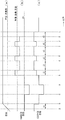
도 3은, 충전을 금지하는 충전 금지 온도와 방전을 금지하는 방전 금지 온도의 설정예를 나타내는 도면이다. 도 3에 있어서, 세로축은 검출 온도를 나타내고, 가로축은 충방전 제어 회로의 온도 검출 단자의 전압을 나타내고 있다. 도 3의 예에서는, 고온 방전 금지 온도(THD), 고온 충전 금지 온도(THC), 저온 방전 금지 온도(TCD) 및 저온 충전 금지 온도(TCC)의 각각이 설정되어 있다.3 is a diagram showing an example of setting a charge prohibition temperature for prohibiting charging and a discharge prohibition temperature for prohibiting discharge. In Fig. 3, the vertical axis represents the detection temperature, and the horizontal axis represents the voltage of the temperature detection terminal of the charge/discharge control circuit. In the example of FIG. 3, each of the high-temperature discharge prohibition temperature THD, the high-temperature charge prohibition temperature THC, the low-temperature discharge prohibition temperature TCD, and the low-temperature charge prohibition temperature TCC are set.
여기서, 고온 방전 금지 온도(THD)>고온 충전 금지 온도(THC)의 관계이기 때문에, 온도가 고온 충전 금지 온도(THC)를 웃돌면 충전은 금지되지만 방전은 금지되지 않으며, 고온 방전 금지 온도(THD)를 웃돌면 충전과 함께 방전도 금지된다.Here, since it is a relationship between the high-temperature discharge prohibition temperature (THD)> the high-temperature charge prohibition temperature (THC), if the temperature exceeds the high-temperature charge prohibition temperature (THC), charging is prohibited but discharge is not prohibited, and the high-temperature discharge prohibition temperature (THD) If it exceeds, charging and discharging are also prohibited.
한편, 저온 방전 금지 온도(TCD)<저온 충전 금지 온도(TCC)의 관계이기 때문에, 온도가 저온 충전 금지 온도(TCC)를 밑돌면 충전은 금지되지만 방전은 금지되지 않으며, 저온 방전 금지 온도(TCD)를 밑돌면 충전과 함께 방전도 금지된다.On the other hand, since there is a relationship between the low temperature discharge prohibition temperature (TCD) <the low temperature charge prohibition temperature (TCC), if the temperature is less than the low temperature charge prohibition temperature (TCC), charging is prohibited but discharge is not prohibited, and the low temperature discharge prohibition temperature (TCD) If it is less than, charging and discharging are also prohibited.
도 4는, 배터리 장치에 있어서의 배터리에 대한 충전 및 방전의 제어예를 설명하는 회로도이다. 배터리 장치(550)에는, 배터리(400) 및 충방전 제어 장치(560)가 구비되어 있다. 충방전 제어 장치(560)에는, 충방전 제어 회로(500), 방전 제어 FET(101), 충전 제어 FET(102) 및 온도 검출 소자(103) 각각이 구비되어 있다.4 is a circuit diagram for explaining an example of controlling charging and discharging of a battery in a battery device. The
온도 보호 기능에 의한 충전 금지 상태에 있어서, 배터리(400)로부터 부하(201)에 대해서 방전을 행할 때, 방전 제어 FET(101)를 온, 충전 제어 FET(102)를 오프로 했을 경우, 충전 제어 FET의 보디 다이오드(102D)를 개재한 방전 전류가 흐른다.When discharging the
FET의 채널의 저항값보다 보디 다이오드의 저항값이 높기 때문에, 방전 전류가 보디 다이오드(102D)에 흐름으로써, 충전 제어 FET(102)에 있어서의 소비 전력이 증가하여, 충전 제어 FET(102)가 발열해 버려, 과도한 온도 상승에 의해 손상을 입을 우려가 있다.Since the resistance value of the body diode is higher than the resistance value of the channel of the FET, the discharge current flows through the
그 때문에, 부하(201)가 접속되어, 방전 전류가 흐르고 있는 경우, 방전 제어 FET(101)뿐만 아니라, 충전 제어 FET(102)도 온시킬 필요가 있다.Therefore, when the
특허 문헌 1에 있어서는, 방전 전류가 흐르고 있는 것을 검출하기 위해, 소정의 주기마다, CO단자(502)로부터 VM단자(501)의 전압을 출력하고, 충전 제어 FET(102)를 일단 오프시켜, VM단자(501)의 전압의 계측을 행하고 있다.In
그리고, VM단자(501)의 전압이 미리 설정한 부하 검출 전압을 웃돌고 있는지 여부에 의해, 방전 전류가 흐르고 있는지 여부의 판정을 행하고 있다.Then, based on whether the voltage of the
이것에 의해, 충방전 제어 회로(500)는, 충전 제어 FET(102)를 단시간 오프시켜, 보디 다이오드(102D)에 발생하는 전압을 검출함으로써, 방전 전류가 흐르고 있는 것을 판정한다.Thereby, the charge/
여기서, 보디 다이오드(102D)에 방전 전류를 흐르게 하는 것은 단시간이기 때문에, 충전 제어 FET(102)가 소비 전력의 증가에 의해 발열할 우려는 없다.Here, since it is a short time for the discharge current to flow through the
이와 같이 하여, 충전 금지 상태의 경우, 소정의 주기로 방전 전류가 흐르고 있는지 여부의 판정을 행하고 있다.In this way, in the case of the charging prohibition state, it is determined whether or not the discharge current flows in a predetermined cycle.
도 5는, 상술한 충전 금지 상태에 있어서의 충방전 제어의 동작예를 설명하는 타이밍 차트이다. 타이밍 차트 (a)에서는, 세로축은 온도 검출 소자의 온도를 나타내고, 가로축은 시간을 나타내고 있다. 타이밍 차트 (b)에서는, 세로축은 VM단자(501)의 전압을 나타내고, 가로축은 시간을 나타내고 있다. 타이밍 차트 (c)에서는, 세로축은 CO단자(502)의 전압을 나타내고, 가로축은 시간을 나타내고 있다. 이하의 설명에 있어서는, 검출 온도가 고온 충전 금지 온도를 초과한 충전 금지 상태의 경우에 있어서의 충방전 제어를 예로서 설명한다.5 is a timing chart illustrating an example of operation of charge/discharge control in the above-described charge prohibition state. In the timing chart (a), the vertical axis represents the temperature of the temperature detection element, and the horizontal axis represents time. In the timing chart (b), the vertical axis represents the voltage of the
시각(A):충방전 제어 회로(500)는, 온도가 고온 충전 금지 온도를 웃돈 것을 검출한다.Time (A): The charge/
시각(B):충방전 제어 회로(500)는, 온도가 고온 충전 금지 온도를 웃돈 것을 검출한 후, 시간(t1) 경과 후에 있어서, VM단자(501)의 전압에 의하지 않고, CO단자(502)에 대해서 VM단자의 전압을 출력하여, 충전 제어 FET(102)를 오프시킨다.Time (B): The charge/
시각(C):충전기(202)가 배터리 장치(550)에 접속되었을 때, 충전 제어 FET(102)가 오프되어 있기 때문에, 충전 전류는 흐르지 않으며, VM단자의 전압은, VSS단자(504)의 전압보다 음측으로 하강한다. 이것에 의해, 충방전 제어 회로(500)는, VM단자 전압이 부하 검출 전압 이하이기 때문에, CO단자(502)로부터 VM단자의 전압을 출력하여, 충전 제어 FET(102)를 계속 오프시킨다.Time (C): When the
시각(D):충전기(202)가 배터리 장치(550)로부터 떼어졌을 때, 충전 전류가 흐르지 않기 때문에, VM단자 전압은, VSS단자(504)의 전압과 동(同)전위가 된다. 충방전 제어 회로(500)는, VM단자의 전압이 부하 검출 전압 이하이기 때문에, CO단자(502)로부터 VM단자의 전압을 출력하여, 충전 제어 FET(102)를 계속 오프시킨다.Time (D): When the
시각(E):부하(201)가 배터리 장치(550)에 접속되었을 때, 방전 제어 FET(101)가 온이기 때문에 방전 전류가 흐른다. 이 때, 충전 제어 FET(102)가 오프이기 때문에, 방전 전류는 충전 제어 FET(102)의 보디 다이오드(102D)를 개재하여 흐른다. 이것에 의해, VM단자의 전압이 부하 검출 전압을 웃돈다. 이 때, 충방전 제어 회로(500)는, 시간(t2)의 카운트 동작을 개시한다.Time (E): When the
시각(F):충방전 제어 회로(500)는, 카운트가 시간(t2)을 경과하면, CO단자(502)로부터 VDD단자(505)의 전압을 출력하여, 충전 제어 FET(102)를 온시킨다. 이것에 의해, 방전 전류는, 충전 제어 FET(102)의 채널을 흐른다. 이 때문에, 방전 전류가 보디 다이오드(102D)에 흐르지 않게 되어, VM단자의 전압은 하강한다. 또한, 충방전 제어 회로(500)는, 시간(t3)의 카운트 동작을 개시한다.Time (F): When the count passes the time (t2), the charge/
시각(G):충방전 제어 회로(500)는, 카운트가 시간(t3)을 경과하면, CO단자(502)로부터 VM단자의 전압을 출력하여, 충전 제어 FET(102)를 오프시킨다.Time (G): When the count passes the time t3, the charge/
그리고, 충방전 제어 회로(500)는, VM단자의 전압이 부하 검출 전압을 웃돌고 있는지 여부에 의해, 방전 전류가 흐르고 있는지 여부의 판정을 행한다. 이 때, 방전 전류가 보디 다이오드(102D)를 흐르고 있기 때문에, VM단자의 전압은 부하 검출 전압을 초과하고 있다. 이 때문에, 충방전 제어 회로(500)는, 시간(t2)의 카운트 동작을 개시한다.Then, the charge/
상술한 바와 같이, 특허 문헌 1에 있어서의 충방전 제어는, 방전 전류가 충방전 FET(102)의 보디 다이오드(102D)에 발생하는 전압에 의해 상승한 VM단자의 전압이 부하 검출 전압을 웃도는지 여부에 의해, 방전 전류가 흐르고 있는지 여부의 판정을 행하고 있다.As described above, the charge/discharge control in
이것에 의해, 충전 금지 상태에 있어서의 방전 전류가, 보디 다이오드(102D)를 계속 흐르는 것을 방지하여, 소비 전력의 증가에 의한 충전 제어 FET(102)의 발열을 억제하고 있다.This prevents the discharge current in the charging prohibition state from continuing to flow through the
그러나, 특허 문헌 1에 의한 충방전 제어는, 방전 전류가 흐르고 있는지 여부를 판정하기 위해서, 충전 제어 FET(102)를 온으로부터 일단 오프시키기 때문에, 부하(201)에 대해서 출력하는 전압에 리플형의 노이즈가 발생한다. 용도에 따라서는, 발생한 노이즈가 기기에 악영향을 줄 우려가 있다.However, in the charge/discharge control according to
또한, 상술한 예와는 방전 금지 온도와 충전 금지 온도의 설정이 반대의 경우, 방전 금지 상태에 있어서 충전을 행하는 것이 가능하다. 이 때문에, 충전 제어 FET(102)를 온으로 하여, 방전 제어 FET(101)의 온/오프 제어를 행하고, 충전 전류가 방전 제어 FET(101)의 보디 다이오드(101D)를 흐르는 것에 의한 VM단자 전압의 변화를 검출하여, 충전기(202)가 접속되어 충전 전류가 흐르고 있는지 여부의 판정을 행한다. 이 경우에도, 이미 서술한 충전 금지 상태에 있어서의 방전 전류에 의한 충전 제어 FET(102)의 발열과 마찬가지로 방전 금지 상태에 있어서의 충전 전류에 의한 방전 제어 FET(101)의 발열이 있다.In addition, when the setting of the discharge prohibition temperature and the charge prohibition temperature is opposite to the above-described example, charging can be performed in the discharge prohibition state. Therefore, the
본 발명은, 이러한 사정을 감안하여 이루어진 것으로, 방전 전류가 흐르고 있는지 여부의 판정을 충전 제어 FET의 온/오프를 반복하여 충전 제어 FET의 보디 다이오드에 방전 전류를 흐르게 하여 행하는 것, 혹은 충전 전류가 흐르고 있는지 여부를, 방전 제어 FET의 온/오프를 반복하여 방전 제어 FET의 보디 다이오드에 충전 전류를 흐르게 하여 행하는 것 중 어느 쪽도 하지 않고, 충전 금지 상태에 있어서의 방전 제어, 방전 금지 상태에 있어서의 충전 제어를 행할 수 있는 충방전 제어 회로, 충방전 제어 장치 및 배터리 장치를 제공한다.The present invention has been made in view of these circumstances, and the determination of whether or not a discharge current is flowing is performed by repeatedly turning on/off the charge control FET to flow the discharge current through the body diode of the charge control FET, or Whether it is flowing or not is performed by repeatedly turning on/off the discharge control FET to flow a charging current through the body diode of the discharge control FET, and in the discharge control in the charge prohibition state or in the discharge prohibition state. A charge/discharge control circuit, a charge/discharge control device, and a battery device capable of controlling the charge and discharge of the battery are provided.
본 발명의 한 양태에 따른 충방전 제어 회로는, 배터리의 양극 단자에 접속되는 양극 전원 단자와, 상기 배터리의 음극 단자에 접속되는 음극 전원 단자와, 상기 배터리의 충방전 경로의 전압과 미리 설정된 충방전 판정 전압에 의거하여, 상기 배터리에 방전 전류가 흐르고 있는 방전 상태와, 상기 배터리에 충전 전류가 흐르고 있는 충전 상태를 판정하는 충방전 판정 회로와, 충전 금지 상태 또한 상기 방전 상태인 경우에 방전 제어 FET 및 충전 제어 FET를 온하고, 상기 충전 금지 상태 또한 상기 충전 상태인 경우에 상기 충전 제어 FET를 오프하는 제어 회로를 구비하는 것을 특징으로 한다.The charge/discharge control circuit according to an aspect of the present invention includes a positive power terminal connected to a positive terminal of a battery, a negative power terminal connected to a negative terminal of the battery, a voltage of a charge/discharge path of the battery, and a preset charge. Based on the discharge determination voltage, a charge/discharge determination circuit for determining a discharge state in which a discharge current flows through the battery and a charge state in which a charge current flows in the battery, and a discharge control when the charge prohibition state is also the discharge state And a control circuit that turns on the FET and the charge control FET and turns off the charge control FET when the charge prohibition state is also the charge state.
본 발명의 다른 양태에 따른 충방전 제어 회로는, 배터리의 양극 단자에 접속되는 양극 전원 단자와, 상기 배터리의 음극 단자에 접속되는 음극 전원 단자와, 상기 배터리의 충방전 경로의 전압과 미리 설정된 충방전 판정 전압에 의거하여, 상기 배터리에 충전 전류가 흐르고 있는 충전 상태와, 상기 배터리에 방전 전류가 흐르고 있는 방전 상태를 판정하는 충방전 판정 회로와, 방전 금지 상태 또한 상기 충전 상태인 경우에 방전 제어 FET 및 충전 제어 FET를 온하고, 상기 방전 금지 상태 또한 상기 방전 상태인 경우에 상기 방전 제어 FET를 오프하는 제어 회로를 구비하는 것을 특징으로 한다.The charge/discharge control circuit according to another aspect of the present invention includes a positive power terminal connected to a positive terminal of a battery, a negative power terminal connected to a negative terminal of the battery, a voltage of a charge/discharge path of the battery, and a preset charge. Based on the discharge determination voltage, a charge/discharge determination circuit for determining a state of charge in which a charging current flows through the battery and a discharge state in which a discharge current flows through the battery, and a discharge control when the discharge prohibition state is also the charge state And a control circuit that turns on the FET and the charge control FET and turns off the discharge control FET when the discharge prohibition state is also the discharge state.
이 발명에 의하면, 방전 전류가 흐르고 있는지 여부의 판정을 충전 제어 FET의 온/오프를 반복하여 충전 제어 FET의 보디 다이오드에 방전 전류를 흐르게 하여 행하거나, 혹은 충전 전류가 흐르고 있는지 여부를, 방전 제어 FET의 온/오프를 반복하여 방전 제어 FET의 보디 다이오드에 충전 전류를 흐르게 하여 행하지 않고, 충전 금지 상태에 있어서의 방전 제어, 방전 금지 상태에 있어서의 충전 제어를 행할 수 있는 충방전 제어 회로, 충방전 제어 장치 및 배터리 장치를 제공할 수 있다.According to this invention, the determination of whether or not the discharge current is flowing is performed by repeatedly turning on/off the charge control FET to flow the discharge current through the body diode of the charge control FET, or to determine whether the charge current is flowing or not, the discharge control A charge/discharge control circuit capable of performing discharge control in a charge prohibition state and charge control in a discharge prohibition state without flowing a charging current through the body diode of the FET by repeatedly turning on/off the FET. A discharge control device and a battery device can be provided.
도 1은, 본 발명의 실시 형태에 의한 충방전 제어 회로를 구비한 배터리 장치의 구성예를 나타내는 회로도이다.
도 2는, 본 실시 형태에 의한 충방전 제어 회로를 구비한 배터리 장치의 동작예를 설명하는 파형도이다.
도 3은, 충전을 금지하는 충전 금지 온도와 방전을 금지하는 방전 금지 온도의 설정예를 나타내는 도면이다.
도 4는, 배터리 장치에 있어서의 배터리에 대한 충전 및 방전의 제어예를 설명하는 회로도이다.
도 5는, 상술한 충전 금지 상태에 있어서의 충방전 제어의 동작예를 설명하는 타이밍 차트이다.1 is a circuit diagram showing a configuration example of a battery device including a charge/discharge control circuit according to an embodiment of the present invention.
2 is a waveform diagram illustrating an operation example of the battery device including the charge/discharge control circuit according to the present embodiment.
3 is a diagram showing an example of setting a charge prohibition temperature for prohibiting charging and a discharge prohibition temperature for prohibiting discharge.
4 is a circuit diagram for explaining an example of controlling charging and discharging of a battery in a battery device.
5 is a timing chart illustrating an example of operation of charge/discharge control in the above-described charge prohibition state.
<제1의 실시 형태><First embodiment>
이하, 도면을 참조하여, 본 발명의 제1의 실시 형태에 대해 설명한다.Hereinafter, a first embodiment of the present invention will be described with reference to the drawings.
도 1은, 본 실시 형태에 의한 충방전 제어 회로 및 충방전 제어 장치를 구비한 배터리 장치의 구성예를 나타내는 회로도이다.1 is a circuit diagram showing a configuration example of a battery device including a charge/discharge control circuit and a charge/discharge control device according to the present embodiment.
이 도 1에 있어서, 배터리 장치(401)에는, 배터리(400) 및 충방전 제어 장치(360)가 구비되어 있다. 충방전 제어 장치(360)에는, 충방전 제어 회로(300), 방전 제어 FET(101), 충전 제어 FET(102) 및 온도 검출 소자(103)가 구비되어 있다.In this FIG. 1, the
또한, 충방전 제어 회로(300)는, 출력 회로(311), 제어 회로(312), 온도 검출 회로(313) 및 충방전 판정 회로(314)를 구비하고 있다.Further, the charge/
배터리 장치(401)는, 외부 양극 단자(351)와 외부 음극 단자(352)를 갖고 있다. 또한, 배터리 장치(401)는, 외부 양극 단자(351)와 외부 음극 단자(352)의 사이에 부하(201)가 접속되어 있는 경우, 배터리(400)로부터 부하(201)에 대해서 방전을 행한다. 한편, 배터리 장치(401)는, 외부 양극 단자(351)와 외부 음극 단자(352)의 사이에 충전기(202)가 접속되어 있는 경우, 배터리(400)에 대한 충전을 행한다. 배터리 장치(401)에 있어서의 배터리(400)의 충방전 경로는, 외부 양극 단자(351)와 외부 음극 단자(352)의 사이이며, 배터리(400)에 충전 전류를 흐르게 하거나 혹은 방전 전류를 흐르게 하는 방전 제어 FET(101), 충전 제어 FET(102)가 직렬로 끼워진 경로이다.The
충방전 제어 회로(300)는, 외부 음전압 입력 단자(301), 충전 제어 단자(302), 방전 제어 단자(304), 온도 검출 단자(303), 양극 전원 단자(305) 및 음극 전원 단자(306)를 구비하고 있다.The charge/
방전 제어 FET(101)는, N채널형 FET이며, 소스 및 백 게이트가 음극 전원 단자(306)에 접속되고, 게이트가 방전 제어 단자(304)에 접속되어 있다. 또한, 방전 제어 FET(101)는, 소스를 애노드로 하고, 드레인을 캐소드로 하는 보디 다이오드(101D)를 갖고 있다.The
충전 제어 FET(102)는, N채널형 FET이며, 소스 및 백 게이트가 외부 음극 단자(352)와 외부 음전압 입력 단자(301)에 접속되고, 게이트가 충전 제어 단자(302)에 접속되며, 드레인이 방전 제어 FET(101)의 드레인에 접속되어 있다. 또한, 충전 제어 FET(102)는, 소스를 애노드로 하고, 드레인을 캐소드로 하는 보디 다이오드(102D)를 갖고 있다.The
배터리(400)는, 양극 단자가 양극 전원 단자(305) 및 외부 양극 단자(351)에 접속되고, 음극 단자가 음극 전원 단자(306) 및 방전 제어 FET(101)의 소스 및 백 게이트에 접속되어 있다.In the
온도 검출 소자(103)는, 예를 들면 NTC 서미스터 소자이며, 배터리(400), 방전 제어 FET(101), 충전 제어 FET(102), 충방전 제어 회로(300)의 기판, 배터리 장치(401)의 하우징 등의 배치된 장소의 온도에 대응한 저항값으로 변화한다. 충방전 제어 회로(300)는, 온도 검출 단자(303)를 개재하여 그 저항값을 측정하고, 내부에서 설정한 충전 금지 온도, 방전 금지 온도를 웃돌고 있는지, 밑돌고 있는지를 판정한다.The
출력 회로(311)는, 제어 회로(312)로부터 공급되는 충전 금지 신호 및 방전 금지 신호에 의해, 방전 제어 FET(101) 및 충전 제어 FET(102)의 온/오프 제어를 행한다.The
출력 회로(311)는, 충전 금지 신호 및 방전 금지 신호 모두 공급되지 않는 경우, 충전 제어 단자(302) 및 방전 제어 단자(304)에 양극 전원 단자(305)의 전압을 출력한다.The
출력 회로(311)는, 충전 금지 신호가 공급되었을 경우, 충전 제어 단자(302)에 대해서 외부 음전압 입력 단자(301)의 전압을 출력하여, 충전 제어 FET(102)를 오프한다. 또한, 출력 회로(311)는, 방전 금지 신호가 공급되었을 경우, 방전 제어 단자(304)에 음극 전원 단자(306)의 전압을 인가하여, 방전 제어 FET(101)를 오프한다.When the charge prohibition signal is supplied, the
제어 회로(312)는, 온도 검출 회로(313)로부터 공급되는, 내부에서 설정한 충전 금지 온도, 방전 금지 온도를 웃돌고 있는지, 밑돌고 있는지를 나타내는 신호에 따라서, 지연 시간의 계측과 상태 판정을 실시하여 온도에 의한 충방전 제어를 행한다.The
제어 회로(312)는, 온도에 의한 방전 금지 상태 및 온도에 의한 충전 금지 상태 중 어느 쪽도 아닌 통상 상태의 경우, 충방전 판정 회로(314)로부터 공급되는 충방전 판정 신호에 의하지 않고, 충전 금지 신호 및 방전 금지 신호 모두 출력하지 않으며, 충전, 방전 모두 허가한다.The
한편, 제어 회로(312)는, 온도에 의한 방전 금지 상태가 아닌 온도에 의한 충전 금지 상태이며, 충방전 판정 회로(314)로부터 공급되는 충방전 판정 신호가 충전을 나타내고 있는 경우, 충전 금지 신호를 출력 회로(311)에 출력하여, 충전을 금지한다.On the other hand, the
또한, 제어 회로(312)는, 온도에 의한 방전 금지 상태가 아닌 온도에 의한 충전 금지 상태이며, 충방전 판정 회로(314)로부터 공급되는 충방전 판정 신호가 방전을 나타내고 있는 경우, 충전 금지 신호 및 방전 금지 신호 모두 출력하지 않는다.In addition, the
또한, 제어 회로(312)는, 시간의 카운트를 행하여, 카운트한 시간이 미리 설정된 설정 시간인 시간(t1)을 경과했는지 여부의 판정을 행한다.Further, the
마찬가지로, 제어 회로(312)는, 시간의 카운트를 행하여, 카운트한 시간이 미리 설정된 설정 시간인 시간(t2)을 경과했는지 여부를 판정한다.Similarly, the
온도 검출 회로(313)는, 온도 검출 단자(303)를 개재하여 온도 검출 소자(103)의 저항값에 의해 발생하는 전압을 측정하여, 현재의 온도와 고온 방전 금지 온도(THD), 고온 충전 금지 온도(THC), 저온 충전 금지 온도(TCC), 저온 방전 금지 온도(TCD)의 설정 전압의 비교를 행한다.The
그리고, 온도 검출 회로(313)에는, 상술한 고온 방전 금지 온도(THD), 고온 충전 금지 온도(THC), 저온 방전 금지 온도(TCD) 및 저온 충전 금지 온도(TCC)의 각각이, 도 3에 나타나고 있는 대응 관계로 미리 설정되어 있다. 이 도 3은, 충전을 금지하는 충전 금지 온도와 방전을 금지하는 방전 금지 온도의 설정예이며, 세로축은 온도 검출 소자(103)가 검출하는 온도를 나타내고, 가로축은 충방전 제어 회로(300)의 온도 검출 단자(303)의 전압을 나타내고 있다.In the
상술한 도 3에 대응하여, 온도 검출 회로(313)는, 현재의 온도가 고온 충전 금지 온도(THC)를 밑돌고, 또한 저온 충전 금지 온도(TCC)를 웃돌고 있는 경우, 그것을 나타내는 신호를 제어 회로(312)에 출력한다.Corresponding to the above-described FIG. 3, when the current temperature is lower than the high temperature charging prohibition temperature THC and exceeds the low temperature charging prohibition temperature TCC, the
그리고, 제어 회로(312)는, 현재의 온도가 고온 충전 금지 온도(THC)를 밑돌고, 또한 현재의 온도가 저온 충전 금지 온도(TCC)를 웃돌고 있기 때문에, 통상 상태라고 판정하여, 충전 금지 신호 및 방전 금지 신호 모두 출력 회로(311)에 출력하지 않는다.Then, the
또한, 온도 검출 회로(313)는, 현재의 온도가 고온 충전 금지 온도(THC) 이상인 경우, 또한 현재의 온도가 저온 충전 금지 온도(TCC) 이하인 경우, 그것을 나타내는 신호를 제어 회로(312)에 출력한다.Further, the
그리고, 제어 회로(312)는, 현재의 온도가 고온 충전 금지 온도(THC) 이상, 또는 저온 충전 금지 온도(TCC) 이하 중 어느 하나이기 때문에, 충전 금지 상태라고 판정하여, 충전 금지 신호를 출력 회로(311)에 출력한다.Then, the
또한, 온도 검출 회로(313)는, 현재의 온도가 고온 방전 금지 온도(THD) 이상인 경우, 또한 현재의 온도가 저온 방전 금지 온도(TCD) 이하인 경우, 그것을 나타내는 신호를 제어 회로(312)에 출력한다.Further, the
그리고, 제어 회로(312)는, 현재의 온도가 고온 방전 금지 온도(THD) 이상, 또는 저온 방전 금지 온도(TCD) 이하 중 어느 하나이기 때문에, 방전 금지 상태라고 판정하여, 방전 금지 신호를 출력 회로(311)에 출력한다.Then, the
충방전 판정 회로(314)는, 외부 음전압 입력 단자(301)의 전압과, 미리 설정된 충방전 판정 전압(VJD)의 비교를 행한다.The charge/
그리고, 충방전 판정 회로(314)는, 방전 제어 FET(101) 및 충전 제어 FET(102)가 온인 경우에 있어서, 외부 음전압 입력 단자(301)의 전압이 미리 설정된 충방전 판정 전압(VJD) 이상인 경우에, 방전 전류가 흐르고 있다고 판정한다. 이 때, 충방전 판정 회로(314)는, 방전을 나타내는 신호를, 제어 회로(312)에 대해서 출력한다.And, the charge/
한편, 충방전 판정 회로(314)는, 방전 제어 FET(101) 및 충전 제어 FET(102)가 온인 경우에 있어서, 외부 음전압 입력 단자(301)의 전압이 미리 설정된 충방전 판정 전압(VJD)을 밑돌 경우에, 충전 전류가 흐르고 있다고 판정한다. 이 때, 충방전 판정 회로(314)는, 충전을 나타내는 신호를, 제어 회로(312)에 대해서 출력한다.On the other hand, the charge/
충방전 판정 전압(VJD)은, 음극 전원 단자(306)의 전압으로 설정하는 것이 이상적이다. 충전 전류는 배터리(400)의 음극으로부터 외부 음극 단자(352)의 방향으로 흐르기 때문에, 충전 전류가 흐르면, 외부 음전압 입력 단자(301)의 전압은, 음극 전원 단자(306)의 전압을 밑돌고, 방전 전류는 외부 음극 단자(352)로부터 배터리(400)의 음극의 방향으로 흐르기 때문에 방전 전류가 흐르고 있으면, 외부 음전압 입력 단자(301)의 전압은 음극 전원 단자(306)의 전압을 웃돈다. 이 때문에, 상술한 바와 같이, 충방전 판정 전압(VJD)을 음극 전원 단자(306)의 전압으로 설정하면, 충전 전류가 흐르고 있는지, 방전 전류가 흐르고 있는지를 정확하게 판정하는 것이 가능하게 된다.Ideally, the charge/discharge determination voltage VJD is set to the voltage of the negative
그러나, 제조 편차에 의해, 충방전 판정 전압(VJD)을 음극 전원 단자(306)의 전압으로 설정하는 것이 곤란하기 때문에, 충전 전류가 흐르고 있는 것을 확실하게 판정할 경우, 음극 전원 단자(306)의 전압에 대해서, 소정의 전압(α)을 여유 있게 상승시킨 전압을 충방전 판정 전압(VJD)으로 한다.However, because it is difficult to set the charge/discharge determination voltage VJD to the voltage of the negative
한편, 방전 전류가 흐르고 있는 것을 확실하게 판정할 경우, 음극 전원 단자(306)의 전압으로부터, 소정의 전압(α)을 여유 있게 저하시킨 전압을 충방전 판정 전압(VJD)으로 한다.On the other hand, in the case of reliably determining that the discharge current is flowing, the voltage obtained by lowering the predetermined voltage? From the voltage of the negative
본 실시 형태에 있어서는, 충전 전류가 흐르고 있는 것을 확실하게 판정하기 위해, 충방전 판정 전압(VJD)을, 음극 전원 단자(306)의 전압으로부터 소정의 전압(α)을 여유 있게 상승시킨 전압으로서 이용한다.In this embodiment, in order to reliably determine that the charging current is flowing, the charging/discharging determination voltage VJD is used as a voltage obtained by increasing the predetermined voltage α from the voltage of the negative
다음으로, 도면을 참조하여, 본 실시 형태에 의한 충방전 제어 회로의 동작에 대해서 설명한다. 도 2는, 본 실시 형태에 의한 충방전 제어 회로를 구비한 배터리 장치의 동작예를 설명하는 파형도이다.Next, an operation of the charge/discharge control circuit according to the present embodiment will be described with reference to the drawings. 2 is a waveform diagram illustrating an operation example of the battery device including the charge/discharge control circuit according to the present embodiment.
시각(A):온도 검출 회로(313)는, 현재의 온도가 고온 충전 금지 온도(THC)를 웃돈 것을 나타내는 신호를, 제어 회로(312)에 대해서 출력한다.Time (A): The
이것에 의해, 제어 회로(312)는, 시간(t1)의 카운트를 개시한다.Thereby, the
이 시점에 있어서, 제어 회로(312)는, 부하(201)에 전류를 흐르게 하기 위해, 출력 회로에 대해서, 충전 제어 단자(302) 및 방전 제어 단자(304)로, 양극 전원 단자(305)의 전압을 출력시킨다. 이 때문에, 방전 제어 FET(101) 및 충전 제어 FET(102)가 온이며, 방전 전류가 흐르고 있다.At this point, the
시각(B):제어 회로(312)는, 카운트하는 시간이 미리 설정된 시간(t1)을 경과했기 때문에, 통상 상태로부터 충전 금지 상태로 제어를 변화시킨다.Time (B): The
이 때, 충방전 판정 회로(314)는, 외부 음전압 입력 단자(301)의 전압이 충방전 판정 전압(VJD) 이상이기 때문에, 방전을 나타내는 신호를, 제어 회로(312)에 대해서 출력하고 있다.At this time, the charge/
이 때문에, 제어 회로(312)는, 출력 회로(311)에 대해서, 충전 금지 신호 및 방전 금지 신호 모두 출력하지 않으며, 충전, 방전 모두 허가한다.For this reason, the
이것에 의해, 출력 회로(311)는, 방전 제어 단자(304) 및 충전 제어 단자(302)에 대해서, 양극 전원 단자(305)의 전압을 출력하여, 방전 제어 FET(101) 및 충전 제어 FET(102)를 온하여 방전 전류를 계속 흐르게 한다.Thereby, the
시각(C):이 시점에 있어서, 충전기(202)가 접속된다.Time (C): At this time, the
이것에 의해, 온으로 되어 있는 방전 제어 FET(101) 및 충전 제어 FET(102)를 개재하여 충전 전류가 흐르기 때문에, 방전 제어 FET(101) 및 충전 제어 FET(102)의 채널의 저항값에 의해 발생하는 전압에 의해, 외부 음전압 입력 단자(301)의 전압이 저하하고 충방전 판정 전압(VJD)을 밑돈다.As a result, since the charging current flows through the
이 때, 충방전 판정 회로(314)는, 외부 음전압 입력 단자(301)의 전압이 충방전 판정 전압(VJD)을 밑돈 것을 검출하고, 충전을 나타내는 신호를, 제어 회로(312)에 대해서 출력한다.At this time, the charge/
그리고, 제어 회로(312)는, 충전 금지 상태이기 때문에, 충전을 나타내는 신호가 충방전 판정 회로(314)로부터 공급됨으로써, 충전 금지 신호를 출력 회로(311)에 대해서 출력한다.Then, since the
이것에 의해, 출력 회로(311)는, 충전 제어 단자(302)에 대해서, 외부 음전압 입력 단자(301)의 전압을 인가하여 충전 제어 FET(102)를 오프한다.Thereby, the
시각(D):이 시점에 있어서, 충전기(202)가 배터리 장치(350)로부터 개방된다.Time (D): At this time, the
이것에 의해, 온되어 있는 방전 제어 FET(101)와, 오프되어 있는 충전 제어 FET(102)의 보디 다이오드(102D)를 개재하여 방전 전류가 흐른다. 이 때문에, 방전 제어 FET(101)와 충전 제어 FET(102)의 보디 다이오드(102D)에 발생하는 전압에 의해, 외부 음전압 입력 단자(301)의 전압이 상승하여 충방전 판정 전압(VJD) 이상이 된다.Accordingly, a discharge current flows through the
이 때, 충방전 판정 회로(314)는, 외부 음전압 입력 단자(301)의 전압이 충방전 판정 전압(VJD) 이상이 된 것을 검출하고, 방전 상태를 나타내는 신호를, 제어 회로(312)에 대해서 출력한다. 여기서, 제어 회로(312)는, 출력 회로(311)에 대한 충전 금지 신호의 출력을 유지한다.At this time, the charge/
이것에 의해, 제어 회로(312)는, 미리 설정된 시간(t2)의 카운트를 개시한다.Thereby, the
시각(E):제어 회로(312)는, 카운트하는 시간이 미리 설정된 시간(t2)을 경과했을 경우, 출력 회로(311)에 대한 충전 금지 신호의 출력을 정지한다.Time (E): The
그리고, 출력 회로(311)는, 충전 제어 단자(302)에 대해서, 양극 전원 단자(305)의 전압을 출력하여, 충전 제어 FET(102)를 온시킨다.And the
이것에 의해, 방전 전류가 충전 제어 FET(102)의 채널을 흐르기 때문에, 외부 음전압 입력 단자(301)의 전압은 하강하지만, 방전 제어 FET(101) 및 충전 제어 FET(102)에 발생하는 전압에 의해, 충방전 판정 전압(VJD) 이상이 유지된다. 이 때문에, 충방전 판정 회로(314)는, 제어 회로(312)에 대해서, 방전을 나타내는 신호를 출력한다.Accordingly, since the discharge current flows through the channel of the
시각(F):이 시점에 있어서, 부하(201)가 배터리 장치(350)로부터 개방되어, 부하(201) 및 충전기(202) 모두가 접속되지 않는 상태가 된다.Time (F): At this point in time, the
이 때문에, 방전 전류가 흐르지 않게 되어, 외부 음전압 입력 단자(301)의 전압이 하강하고, 방전 제어 FET(101) 및 충전 제어 FET(102)에 발생하는 전압에 의해, 충방전 판정 전압(VJD)을 밑돈다.Therefore, the discharge current does not flow, the voltage of the external negative
그리고, 충방전 판정 회로(314)는, 충전을 나타내는 신호를 제어 회로(312)에 대해서 출력한다.Then, the charge/
그리고, 제어 회로(312)는, 충전 금지 상태이기 때문에, 충전을 나타내는 신호가 충방전 판정 회로(314)로부터 공급됨으로써, 출력 회로(311)에 대해서 충전 금지 신호를 출력한다.Then, since the
이것에 의해, 출력 회로(311)는, 충전 제어 단자(302)에, 외부 음전압 입력 단자(301)의 전압을 출력하여 충전 제어 FET(102)를 오프한다.Thereby, the
상술한 바와 같이, 본 실시 형태는, 고온 충전 금지 온도(THC)>검출 온도≥고온 방전 금지 온도(THD)로 이루어지는 부등식에 의해 규정되는 충전 금지 상태인 동안, 방전 전류가 흐르고 있는지 여부의 판정을, 외부 음전압 입력 단자(301)의 전압이 충방전 판정 전압(VJD) 이상인지 여부에 의해 충방전 제어 장치(360)가 판정하기 때문에, 충전 제어 FET(102)의 온/오프 제어를 행하지 않고, 충전 금지 상태에서의 방전 제어를 행할 수 있다.As described above, the present embodiment makes a determination as to whether or not a discharge current flows during the charging prohibition state defined by the inequality consisting of the high-temperature charging prohibition temperature (THC)> detection temperature> the high-temperature discharge prohibition temperature (THD). , Since the charge/
이상 설명한 충방전 제어 회로(300)의 동작은, 저온 충전 금지 온도(TCC)<검출 온도≤저온 방전 금지 온도(TCD)로 이루어지는 부등식에 의해 규정되는 충전 금지 상태의 경우에 있어서도 동일하게 행해진다.The operation of the charge/
이것에 의해, 본 실시 형태에 있어서는, 예를 들면, 방전 전류가 흐르고 있을 때, 충전 제어 FET(102)를 오프하지 않기 때문에, 배터리 장치(401)는, 리플형의 노이즈의 발생을 억제할 수 있으며, 접속된 기기로 안정된 전압을 공급하는 것이 가능하게 된다.Accordingly, in the present embodiment, for example, when the discharge current is flowing, the
<제2의 실시 형태><2nd embodiment>
이하, 도면을 참조하여, 제2의 실시 형태에 대해 설명한다. 본 실시 형태의 구성은, 도 1에 나타내는 제1의 실시 형태에 의한 충방전 제어 회로를 구비한 배터리 장치의 구성예와 동일하다. 따라서, 제1의 실시 형태와 중복되는 설명은 생략한다.Hereinafter, a second embodiment will be described with reference to the drawings. The configuration of this embodiment is the same as the configuration example of a battery device including a charge/discharge control circuit according to the first embodiment shown in FIG. 1. Therefore, the description that overlaps with the first embodiment will be omitted.
본 실시 형태에 있어서, 제1의 실시 형태와 다른 점은, 도 3에 의한 고온 방전 금지 온도(THD), 고온 충전 금지 온도(THC), 저온 방전 금지 온도(TCD) 및 저온 충전 금지 온도(TCC)의 각각의 관계가 다른 점이다.In this embodiment, the difference from the first embodiment is the high temperature discharge prohibition temperature (THD), the high temperature charge prohibition temperature (THC), the low temperature discharge prohibition temperature (TCD) and the low temperature charge prohibition temperature (TCC) shown in FIG. Each relationship of) is different.
즉, 본 실시 형태의 경우, 고온 충전 금지 온도(THC)>고온 방전 금지 온도(THD)>저온 방전 금지 온도(TCD)>저온 충전 금지 온도(TCC)로 이루어지는 부등식에 의해 나타내지는 관계가 된다.That is, in the case of the present embodiment, there is a relationship represented by an inequality consisting of the high-temperature charge prohibition temperature (THC)> the high-temperature discharge prohibition temperature (THD)> the low-temperature discharge prohibition temperature (TCD)> the low-temperature charge prohibition temperature (TCC).
이것에 의해, 본 실시 형태에 있어서는, 온도가 고온 방전 금지 온도(THD)를 밑돌고, 또한 저온 방전 금지 온도(TCD)를 웃도는 경우, 충전 및 방전 모두 금지되지 않은 통상 상태이다.Accordingly, in the present embodiment, when the temperature is lower than the high-temperature discharge prohibition temperature THD and exceeds the low-temperature discharge prohibition temperature TCD, both charging and discharging are not prohibited in a normal state.
그리고, 본 실시 형태에 있어서는, 온도가 고온 방전 금지 온도(THD) 이상이며, 또한 고온 충전 금지 온도(THC)를 밑돌 경우, 혹은 온도가 저온 방전 금지 온도(TCD) 이하이며, 또한 저온 충전 금지 온도(TCC)를 웃도는 경우, 방전 금지 상태가 된다.And, in this embodiment, when the temperature is higher than the high temperature discharge prohibition temperature (THD) and below the high temperature charge prohibition temperature (THC), or the temperature is lower than the low temperature discharge prohibition temperature (TCD), and the low temperature charge prohibition temperature When it exceeds (TCC), it becomes a discharge prohibition state.
또한, 본 실시 형태에 있어서는, 온도가 고온 충전 금지 온도(THC) 이상 혹은 저온 충전 금지 온도(TCC) 이하가 되면, 방전 금지 상태 또한 충전 금지 상태가 된다.In addition, in the present embodiment, when the temperature is equal to or higher than the high temperature charging prohibition temperature (THC) or lower than the low temperature charging prohibition temperature (TCC), the discharge prohibition state also becomes a charge prohibition state.
따라서, 본 실시 형태에 있어서는, 온도가 고온 방전 금지 온도(THD) 이상이며, 또한 고온 충전 금지 온도(THC)를 밑돌 경우, 혹은 온도가 저온 방전 금지 온도(TCD) 이하이며, 또한 저온 충전 금지 온도(TCC)를 웃돌 때, 즉 충전이 가능한 방전 금지 상태에 있어서의 배터리(400)에 대한 충전 제어가 대상이다.Therefore, in the present embodiment, when the temperature is higher than the high temperature discharge prohibition temperature (THD) and lower than the high temperature charge prohibition temperature (THC), or the temperature is lower than the low temperature discharge prohibition temperature (TCD), and the low temperature charge prohibition temperature When it exceeds (TCC), that is, charge control for the
그 때문에, 본 실시 형태에 있어서도, 제1의 실시 형태와 마찬가지로, 충방전 판정 전압(VJD)은 음극 전원 단자(306)의 전압으로서 설정한다.Therefore, in this embodiment as well as in the first embodiment, the charge/discharge determination voltage VJD is set as the voltage of the negative
그러나, 제1의 실시 형태와 마찬가지로, 제조 편차에 의해, 충방전 판정 전압(VJD)을 음극 전원 단자(306)의 전압으로 설정하는 것이 곤란하기 때문에, 본 실시 형태에 있어서는, 방전 전류가 흐르고 있는 것을 확실하게 판정하기 위해, 충방전 판정 전압(VJD)을, 음극 전원 단자(306)의 전압으로부터 소정의 전압(α)을 여유 있게 저하시킨 전압으로서 이용한다.However, as in the first embodiment, it is difficult to set the charge/discharge determination voltage VJD to the voltage of the negative
제어 회로(312)는, 온도에 의한 방전 금지 상태 및 온도에 의한 충전 금지 상태 중 어느 쪽도 아닌 통상 상태의 경우, 충방전 판정 회로(314)로부터 공급되는 충방전 판정 신호에 의하지 않고, 충전 금지 신호 및 방전 금지 신호 모두 출력하지 않으며, 충전, 방전 모두 허가한다.The
또한, 제어 회로(312)는, 온도에 의한 충전 금지 상태가 아닌 온도에 의한 방전 금지 상태이며, 충방전 판정 회로(314)로부터 공급되는 충방전 판정 신호가 방전을 나타내고 있는 경우, 출력 회로(311)에 대해서 방전 금지 신호를 출력하여, 방전을 금지한다.In addition, the
또한, 제어 회로(312)는, 온도에 의한 충전 금지 상태가 아닌 온도에 의한 방전 금지 상태이며, 충방전 판정 회로(314)로부터 공급되는 충방전 판정 신호가 충전을 나타내고 있는 경우, 출력 회로(311)에 대해서 방전 금지 신호 및 충전 금지 신호를 출력하지 않는다.In addition, when the
상술한 구성에 의해, 본 실시 형태에 있어서는, 제1의 실시 형태에 있어서의 방전 제어 FET(101)에 대한 제어를 충전 제어 FET(102)에 대해서 행하고, 반대로, 제1의 실시 형태에 있어서의 충전 제어 FET(102)에 대한 제어를 방전 제어 FET(101)에 대해서 행한다.With the above-described configuration, in this embodiment, control of the
이것에 의해, 본 실시 형태는, 고온 방전 금지 온도(THD)≤검출 온도<고온 충전 금지 온도(THC)로 이루어지는 부등식에 의해 규정되는 방전 금지 상태인 동안, 충방전 제어 장치(360)에 충전 전류가 흐르고 있는지 여부의 판정을, 외부 음전압 입력 단자(301)의 전압이 충방전 판정 전압(VJD) 이하인지 여부에 의해 판정하기 때문에, 방전 제어 FET(101)의 온/오프 제어를 행하지 않고, 방전 금지 상태에 있어서의 충전 제어를 행할 수 있다.Thus, in the present embodiment, the charging current is supplied to the charging/discharging
이상 설명한 충방전 제어 회로의 동작은, 저온 충전 금지 온도(TCC)<검출 온도≤저온 방전 금지 온도(TCD)로 이루어지는 부등식에 의해 규정되는 방전 금지 상태의 경우에 있어서도 동일하게 행해진다.The operation of the charge/discharge control circuit described above is similarly performed in the case of a discharge prohibition state defined by an inequality consisting of a low temperature charge prohibition temperature (TCC) <detection temperature ≤ low temperature discharge prohibition temperature (TCD).
이상, 이 발명의 실시 형태에 대해 상세하게 서술해 왔는데, 구체적인 구성은 이 실시 형태에 한정되는 것은 아니며, 이 발명의 요지를 벗어나지 않는 범위의 설계 등도 포함된다.As mentioned above, although the embodiment of this invention has been described in detail, the specific structure is not limited to this embodiment, The design etc. of the range which does not deviate from the gist of this invention are also included.
예를 들면, 충방전 제어 회로는, 온도 검출에 의해 충전 금지 상태 혹은 방전 금지 상태로 천이하는 구성으로 했는데, 온도 검출에 한정하지 않고, 도시하지 않은 외부 장치 등으로부터 공급되는 소정의 외부 신호의 검출 등에 의해 충전 금지 상태 혹은 방전 금지 상태로 천이해도 된다.For example, the charge/discharge control circuit is configured to transition to a charge prohibition state or a discharge prohibition state by temperature detection, but is not limited to temperature detection, and detection of a predetermined external signal supplied from an external device (not shown) It may transition to a charging prohibition state or a discharging prohibition state by the like.
또한, 예를 들면, 충방전 제어 장치는 배터리(400)의 음극측에 충전 제어 FET(102) 및 방전 제어 FET(101)를 구비한 구성으로 했는데, 배터리(400)의 양극측에 충전 제어 FET(102) 및 방전 제어 FET(101)를 구비한 구성으로 해도 된다. 이 경우는, 외부 음전압 입력 단자(301)는 외부 양전압 입력 단자로서 외부 양극 단자(351)측에 접속되고, 충방전 판정 전압(VJD)은 양극 전원 단자(305)의 전압으로 설정한다.In addition, for example, the charge/discharge control device has a configuration including a
또한, 예를 들면, 충방전 판정 회로(314)는 외부 음전압 입력 단자(301)의 전압에 의해 충전 상태와 방전 상태를 판정하는 구성으로 했는데, 과전류 검출 단자의 전압에 의해 충전 상태와 방전 상태를 판정해도 된다. 즉, 충방전 판정 회로는, 충방전 판정 전압과 비교하기 위한, 충전 상태나 방전 상태로 변화하는 충방전 경로의 전압이 입력되면 된다.In addition, for example, the charge/
101 방전 제어 FET
101D, 102D 보디 다이오드
102 충전 제어 FET
103 온도 검출 소자
201 부하
202 충전기
300 충방전 제어 회로
301 외부 음전압 입력 단자
302 충전 제어 단자
303 온도 검출 단자
304 방전 제어 단자
305 양극 전원 단자
306 음극 전원 단자
311 출력 회로
312 제어 회로
313 온도 검출 회로
314 충방전 판정 회로
350 배터리 장치
351 외부 양극 단자
352 외부 음극 단자
360 충방전 제어 장치
400 배터리101 Discharge Control FET
101D, 102D body diode
102 Charge Control FET
103 temperature detection element
201 load
202 charger
300 charge/discharge control circuit
301 external negative voltage input terminal
302 charge control terminal
303 temperature detection terminal
304 discharge control terminal
305 positive power terminal
306 negative power terminal
311 output circuit
312 control circuit
313 temperature detection circuit
314 Charge/discharge judgment circuit
350 battery unit
351 external positive terminal
352 external negative terminal
360 charge/discharge control device
400 battery
Claims (10)
상기 배터리의 음극 단자에 접속되는 음극 전원 단자와,
상기 배터리의 충방전 경로의 전압과 미리 설정된 충방전 판정 전압에 의거하여, 상기 배터리에 방전 전류가 흐르고 있는 방전 상태와, 상기 배터리에 충전 전류가 흐르고 있는 충전 상태를 판정하는 충방전 판정 회로와,
충전 금지 상태 또한 상기 방전 상태인 경우에 방전 제어 FET 및 충전 제어 FET를 온하고, 상기 충전 금지 상태 또한 상기 충전 상태인 경우에 상기 충전 제어 FET를 오프하는 제어 회로를 구비하는 것을 특징으로 하는 충방전 제어 회로.A positive power supply terminal connected to the positive terminal of the battery,
A negative power supply terminal connected to the negative terminal of the battery,
A charge/discharge determination circuit for determining a discharge state in which a discharge current flows in the battery and a charge state in which a charge current flows in the battery based on a voltage of the charge/discharge path of the battery and a preset charge/discharge determination voltage,
Charging and discharging comprising a control circuit that turns on a discharge control FET and a charge control FET when the charge prohibition state is also the discharge state, and turns off the charge control FET when the charge prohibition state is also the charge state. Control circuit.
상기 배터리의 음극 단자에 접속되는 음극 전원 단자와,
상기 배터리의 충방전 경로의 전압과 미리 설정된 충방전 판정 전압에 의거하여, 상기 배터리에 충전 전류가 흐르고 있는 충전 상태와, 상기 배터리에 방전 전류가 흐르고 있는 방전 상태를 판정하는 충방전 판정 회로와,
방전 금지 상태 또한 상기 충전 상태인 경우에 방전 제어 FET 및 충전 제어 FET를 온하고, 상기 방전 금지 상태 또한 상기 방전 상태인 경우에 상기 방전 제어 FET를 오프하는 제어 회로를 구비하는 것을 특징으로 하는 충방전 제어 회로.A positive power supply terminal connected to the positive terminal of the battery,
A negative power supply terminal connected to the negative terminal of the battery,
A charge/discharge determination circuit for determining a state of charge in which a charge current flows through the battery and a discharge state in which a discharge current flows through the battery, based on a voltage of the charge/discharge path of the battery and a preset charge/discharge determination voltage,
Charge/discharge comprising a control circuit for turning on the discharge control FET and the charge control FET when the discharge prohibition state is also the charge state, and turns off the discharge control FET when the discharge prohibition state is also the discharge state. Control circuit.
상기 충방전 판정 전압이 상기 음극 전원 단자의 전압으로 설정되어 있는 것을 특징으로 하는 충방전 제어 회로.The method according to claim 1 or 2,
The charge/discharge control circuit, wherein the charge/discharge determination voltage is set to the voltage of the negative power supply terminal.
상기 충방전 판정 전압이 상기 양극 전원 단자의 전압으로 설정되어 있는 것을 특징으로 하는 충방전 제어 회로.The method according to claim 1 or 2,
The charge/discharge control circuit, wherein the charge/discharge determination voltage is set to the voltage of the positive power supply terminal.
충전의 제어를 행하는 충전 제어 FET와,
청구항 1 또는 청구항 2에 기재된 충방전 제어 회로를 구비하는 것을 특징으로 하는 충방전 제어 장치.A discharge control FET for controlling discharge, and
A charge control FET that controls charge, and
A charge/discharge control device comprising the charge/discharge control circuit according to claim 1 or 2.
충전의 제어를 행하는 충전 제어 FET와,
청구항 3에 기재된 충방전 제어 회로를 구비하는 것을 특징으로 하는 충방전 제어 장치.A discharge control FET for controlling discharge, and
A charge control FET that controls charge, and
A charge/discharge control device comprising the charge/discharge control circuit according to claim 3.
충전의 제어를 행하는 충전 제어 FET와,
청구항 4에 기재된 충방전 제어 회로를 구비하는 것을 특징으로 하는 충방전 제어 장치.A discharge control FET for controlling discharge, and
A charge control FET that controls charge, and
A charge/discharge control device comprising the charge/discharge control circuit according to claim 4.
상기 배터리의 충방전을 제어하는 청구항 5에 기재된 충방전 제어 장치를 구비하는 것을 특징으로 하는 배터리 장치.Battery and
A battery device comprising the charge/discharge control device according to claim 5 for controlling charge and discharge of the battery.
상기 배터리의 충방전을 제어하는 청구항 6에 기재된 충방전 제어 장치를 구비하는 것을 특징으로 하는 배터리 장치.Battery and
A battery device comprising the charge/discharge control device according to claim 6 for controlling charge and discharge of the battery.
상기 배터리의 충방전을 제어하는 청구항 7에 기재된 충방전 제어 장치를 구비하는 것을 특징으로 하는 배터리 장치.Battery and
A battery device comprising the charge/discharge control device according to claim 7 which controls charge and discharge of the battery.
Applications Claiming Priority (2)
| Application Number | Priority Date | Filing Date | Title |
|---|---|---|---|
| JP2019028991A JP2020137287A (en) | 2019-02-21 | 2019-02-21 | Charge/discharge control circuit, charge/discharge control device and battery device |
| JPJP-P-2019-028991 | 2019-02-21 |
Publications (1)
| Publication Number | Publication Date |
|---|---|
| KR20200102369A true KR20200102369A (en) | 2020-08-31 |
Family
ID=72141886
Family Applications (1)
| Application Number | Title | Priority Date | Filing Date |
|---|---|---|---|
| KR1020200020400A KR20200102369A (en) | 2019-02-21 | 2020-02-19 | Charging/discharging control circuit, charging/discharging control device and battery device |
Country Status (5)
| Country | Link |
|---|---|
| US (1) | US11245279B2 (en) |
| JP (1) | JP2020137287A (en) |
| KR (1) | KR20200102369A (en) |
| CN (1) | CN111600344A (en) |
| TW (1) | TWI828837B (en) |
Families Citing this family (1)
| Publication number | Priority date | Publication date | Assignee | Title |
|---|---|---|---|---|
| CN115431799A (en) * | 2022-08-12 | 2022-12-06 | 长春捷翼汽车零部件有限公司 | Charge and discharge control system |
Citations (1)
| Publication number | Priority date | Publication date | Assignee | Title |
|---|---|---|---|---|
| JP2015104217A (en) | 2013-11-25 | 2015-06-04 | ミツミ電機株式会社 | Secondary battery protection circuit, battery protection module, battery pack and processing method |
Family Cites Families (21)
| Publication number | Priority date | Publication date | Assignee | Title |
|---|---|---|---|---|
| JPH10290530A (en) * | 1997-04-15 | 1998-10-27 | Toshiba Battery Co Ltd | Secondary battery protective circuit |
| JPH11234915A (en) * | 1998-02-20 | 1999-08-27 | Fujitsu Ltd | Power supply device with chargeable battery and charge/ discharge method of a plurality of batteries |
| JP3212963B2 (en) * | 1999-03-16 | 2001-09-25 | 松下電器産業株式会社 | Secondary battery control circuit |
| JP3670522B2 (en) * | 1999-07-30 | 2005-07-13 | 富士通株式会社 | Battery pack |
| JP2001057740A (en) * | 1999-08-18 | 2001-02-27 | Matsushita Electric Ind Co Ltd | Battery protecting device |
| US6639386B2 (en) * | 2001-11-02 | 2003-10-28 | Sanyo Electric Co., Ltd. | Rechargeable battery device equipped with life determination function |
| JP4137496B2 (en) * | 2002-04-15 | 2008-08-20 | 富士通株式会社 | Remaining amount prediction method |
| JP4186052B2 (en) * | 2003-03-26 | 2008-11-26 | ミツミ電機株式会社 | Battery pack with charge control function |
| JP4204446B2 (en) * | 2003-11-14 | 2009-01-07 | ソニー株式会社 | Battery pack, battery protection processing device, and activation control method for battery protection processing device |
| JP2005192371A (en) * | 2003-12-26 | 2005-07-14 | Sanyo Electric Co Ltd | Power supply unit |
| US20050237028A1 (en) * | 2004-04-27 | 2005-10-27 | Denning Bruce S | Secondary battery protection circuit with over voltage transient protection |
| JP2007236033A (en) * | 2006-02-27 | 2007-09-13 | Sony Corp | Battery pack and method for protecting battery |
| JP5064776B2 (en) * | 2006-12-07 | 2012-10-31 | 三洋電機株式会社 | Pack battery |
| US7737662B2 (en) * | 2006-12-26 | 2010-06-15 | O2Micro International Ltd. | Power management circuit for battery pack |
| US20130049697A1 (en) * | 2011-08-26 | 2013-02-28 | Guoxing Li | Battery protection integrated circuit architecture |
| JP4977797B1 (en) * | 2011-11-30 | 2012-07-18 | 和征 榊原 | Battery system |
| KR102256300B1 (en) * | 2015-01-08 | 2021-05-26 | 삼성에스디아이 주식회사 | Battery pack |
| JP6041031B1 (en) * | 2015-10-02 | 2016-12-07 | ミツミ電機株式会社 | Secondary battery protection integrated circuit, secondary battery protection device and battery pack |
| CN109155531B (en) * | 2016-07-22 | 2022-04-29 | 株式会社村田制作所 | Battery device, electronic apparatus, electric vehicle, power storage system, and control method |
| JP7023561B2 (en) * | 2016-08-30 | 2022-02-22 | エイブリック株式会社 | Charge / discharge control circuit and battery device equipped with this |
| JP6837899B2 (en) * | 2017-04-13 | 2021-03-03 | エイブリック株式会社 | Charge / discharge control circuit and battery device |
-
2019
- 2019-02-21 JP JP2019028991A patent/JP2020137287A/en active Pending
-
2020
- 2020-01-08 TW TW109100523A patent/TWI828837B/en active
- 2020-02-17 US US16/792,612 patent/US11245279B2/en active Active
- 2020-02-19 CN CN202010101291.9A patent/CN111600344A/en active Pending
- 2020-02-19 KR KR1020200020400A patent/KR20200102369A/en unknown
Patent Citations (1)
| Publication number | Priority date | Publication date | Assignee | Title |
|---|---|---|---|---|
| JP2015104217A (en) | 2013-11-25 | 2015-06-04 | ミツミ電機株式会社 | Secondary battery protection circuit, battery protection module, battery pack and processing method |
Also Published As
| Publication number | Publication date |
|---|---|
| TW202040864A (en) | 2020-11-01 |
| TWI828837B (en) | 2024-01-11 |
| US11245279B2 (en) | 2022-02-08 |
| CN111600344A (en) | 2020-08-28 |
| US20200274384A1 (en) | 2020-08-27 |
| JP2020137287A (en) | 2020-08-31 |
Similar Documents
| Publication | Publication Date | Title |
|---|---|---|
| JP4831171B2 (en) | Battery pack and control method | |
| KR100975279B1 (en) | Overcurrent detecting circuit and its delay circuit | |
| US7816889B2 (en) | Method of charging rechargeable battery and protection circuit for rechargeable battery | |
| US9620982B2 (en) | Comparator circuit, semiconductor device, battery monitoring system, charging prohibition method, and computer-readable medium | |
| KR102049148B1 (en) | Battery device and battery protection method | |
| JP5457206B2 (en) | Battery pack | |
| US8581556B2 (en) | Protection circuit and battery pack having current varying circuit to vary current flowing through power terminal | |
| KR100777884B1 (en) | A charge/discharge control circuit and a charging-type power-supply unit | |
| KR101512535B1 (en) | Battery state monitoring circuit and battery device | |
| WO2008019391A1 (en) | Charge-pump biased battery protection circuit | |
| KR102130290B1 (en) | Charge and discharge control circuit and battery device | |
| KR20170040084A (en) | Secondary battery protection integrated circuit, secondary battery protection apparatus and battery pack | |
| KR20110081785A (en) | Battery pack | |
| JP6263908B2 (en) | Battery protection circuit, battery protection device, battery pack, and battery protection method | |
| US20160308377A1 (en) | Semiconductor device for battery control and battery pack | |
| US8524385B2 (en) | Battery pack | |
| US10074875B2 (en) | Protection circuit for secondary battery, battery protection module, battery pack, and method | |
| KR20140109307A (en) | Battery device | |
| US8378635B2 (en) | Semiconductor device and rechargeable power supply unit | |
| JP5098501B2 (en) | Battery pack | |
| JP2014161186A (en) | Switch circuit, semiconductor device, and battery device | |
| US11742686B2 (en) | Battery device and battery charging system | |
| KR20200102369A (en) | Charging/discharging control circuit, charging/discharging control device and battery device | |
| JP2011239652A (en) | Battery protection device and integrated circuit for battery protection | |
| JP2009183050A (en) | Battery pack |