US7170919B2 - Diode-pumped solid-state laser gain module - Google Patents
Diode-pumped solid-state laser gain module Download PDFInfo
- Publication number
- US7170919B2 US7170919B2 US10/602,057 US60205703A US7170919B2 US 7170919 B2 US7170919 B2 US 7170919B2 US 60205703 A US60205703 A US 60205703A US 7170919 B2 US7170919 B2 US 7170919B2
- Authority
- US
- United States
- Prior art keywords
- slab
- laser
- housing
- spacers
- laser slab
- Prior art date
- Legal status (The legal status is an assumption and is not a legal conclusion. Google has not performed a legal analysis and makes no representation as to the accuracy of the status listed.)
- Expired - Fee Related, expires
Links
- 125000006850 spacer group Chemical group 0.000 claims abstract description 45
- 239000000463 material Substances 0.000 claims description 11
- 238000000034 method Methods 0.000 claims description 11
- 230000006835 compression Effects 0.000 claims description 7
- 238000007906 compression Methods 0.000 claims description 7
- 230000008859 change Effects 0.000 claims description 4
- 239000000110 cooling liquid Substances 0.000 abstract description 22
- 239000002826 coolant Substances 0.000 description 38
- 230000000712 assembly Effects 0.000 description 22
- 238000000429 assembly Methods 0.000 description 22
- 230000005855 radiation Effects 0.000 description 10
- 238000001816 cooling Methods 0.000 description 9
- 230000003287 optical effect Effects 0.000 description 9
- 239000007788 liquid Substances 0.000 description 7
- 238000003491 array Methods 0.000 description 4
- 238000005457 optimization Methods 0.000 description 4
- 229910001220 stainless steel Inorganic materials 0.000 description 4
- 239000010935 stainless steel Substances 0.000 description 4
- 239000000853 adhesive Substances 0.000 description 3
- 230000001070 adhesive effect Effects 0.000 description 3
- 239000004020 conductor Substances 0.000 description 3
- 238000005086 pumping Methods 0.000 description 3
- 238000013519 translation Methods 0.000 description 3
- 230000008901 benefit Effects 0.000 description 2
- 239000000919 ceramic Substances 0.000 description 2
- 239000012530 fluid Substances 0.000 description 2
- 230000017525 heat dissipation Effects 0.000 description 2
- 238000010438 heat treatment Methods 0.000 description 2
- 238000004519 manufacturing process Methods 0.000 description 2
- 238000012986 modification Methods 0.000 description 2
- 230000004048 modification Effects 0.000 description 2
- 229910052582 BN Inorganic materials 0.000 description 1
- PZNSFCLAULLKQX-UHFFFAOYSA-N Boron nitride Chemical compound N#B PZNSFCLAULLKQX-UHFFFAOYSA-N 0.000 description 1
- RYGMFSIKBFXOCR-UHFFFAOYSA-N Copper Chemical compound [Cu] RYGMFSIKBFXOCR-UHFFFAOYSA-N 0.000 description 1
- 229920002449 FKM Polymers 0.000 description 1
- 238000010521 absorption reaction Methods 0.000 description 1
- NIXOWILDQLNWCW-UHFFFAOYSA-N acrylic acid group Chemical group C(C=C)(=O)O NIXOWILDQLNWCW-UHFFFAOYSA-N 0.000 description 1
- 230000009471 action Effects 0.000 description 1
- 238000013459 approach Methods 0.000 description 1
- 230000015556 catabolic process Effects 0.000 description 1
- 238000010276 construction Methods 0.000 description 1
- 239000012809 cooling fluid Substances 0.000 description 1
- 229910052802 copper Inorganic materials 0.000 description 1
- 239000010949 copper Substances 0.000 description 1
- 230000003247 decreasing effect Effects 0.000 description 1
- 238000006731 degradation reaction Methods 0.000 description 1
- 238000012423 maintenance Methods 0.000 description 1
- 229910052751 metal Inorganic materials 0.000 description 1
- 239000002184 metal Substances 0.000 description 1
- 150000002739 metals Chemical class 0.000 description 1
- 238000000206 photolithography Methods 0.000 description 1
- 239000004033 plastic Substances 0.000 description 1
- 229920003023 plastic Polymers 0.000 description 1
- 238000005498 polishing Methods 0.000 description 1
- 229920001296 polysiloxane Polymers 0.000 description 1
- 230000008569 process Effects 0.000 description 1
- 239000008213 purified water Substances 0.000 description 1
- 230000008439 repair process Effects 0.000 description 1
- 229920002379 silicone rubber Polymers 0.000 description 1
- 239000004945 silicone rubber Substances 0.000 description 1
- XLYOFNOQVPJJNP-UHFFFAOYSA-N water Chemical compound O XLYOFNOQVPJJNP-UHFFFAOYSA-N 0.000 description 1
Images


Classifications
-
- H—ELECTRICITY
- H01—ELECTRIC ELEMENTS
- H01S—DEVICES USING THE PROCESS OF LIGHT AMPLIFICATION BY STIMULATED EMISSION OF RADIATION [LASER] TO AMPLIFY OR GENERATE LIGHT; DEVICES USING STIMULATED EMISSION OF ELECTROMAGNETIC RADIATION IN WAVE RANGES OTHER THAN OPTICAL
- H01S3/00—Lasers, i.e. devices using stimulated emission of electromagnetic radiation in the infrared, visible or ultraviolet wave range
- H01S3/02—Constructional details
- H01S3/025—Constructional details of solid state lasers, e.g. housings or mountings
-
- H—ELECTRICITY
- H01—ELECTRIC ELEMENTS
- H01S—DEVICES USING THE PROCESS OF LIGHT AMPLIFICATION BY STIMULATED EMISSION OF RADIATION [LASER] TO AMPLIFY OR GENERATE LIGHT; DEVICES USING STIMULATED EMISSION OF ELECTROMAGNETIC RADIATION IN WAVE RANGES OTHER THAN OPTICAL
- H01S3/00—Lasers, i.e. devices using stimulated emission of electromagnetic radiation in the infrared, visible or ultraviolet wave range
- H01S3/05—Construction or shape of optical resonators; Accommodation of active medium therein; Shape of active medium
- H01S3/06—Construction or shape of active medium
- H01S3/0602—Crystal lasers or glass lasers
- H01S3/0606—Crystal lasers or glass lasers with polygonal cross-section, e.g. slab, prism
-
- H—ELECTRICITY
- H01—ELECTRIC ELEMENTS
- H01S—DEVICES USING THE PROCESS OF LIGHT AMPLIFICATION BY STIMULATED EMISSION OF RADIATION [LASER] TO AMPLIFY OR GENERATE LIGHT; DEVICES USING STIMULATED EMISSION OF ELECTROMAGNETIC RADIATION IN WAVE RANGES OTHER THAN OPTICAL
- H01S3/00—Lasers, i.e. devices using stimulated emission of electromagnetic radiation in the infrared, visible or ultraviolet wave range
- H01S3/09—Processes or apparatus for excitation, e.g. pumping
- H01S3/091—Processes or apparatus for excitation, e.g. pumping using optical pumping
- H01S3/094—Processes or apparatus for excitation, e.g. pumping using optical pumping by coherent light
- H01S3/0941—Processes or apparatus for excitation, e.g. pumping using optical pumping by coherent light of a laser diode
-
- H—ELECTRICITY
- H01—ELECTRIC ELEMENTS
- H01S—DEVICES USING THE PROCESS OF LIGHT AMPLIFICATION BY STIMULATED EMISSION OF RADIATION [LASER] TO AMPLIFY OR GENERATE LIGHT; DEVICES USING STIMULATED EMISSION OF ELECTROMAGNETIC RADIATION IN WAVE RANGES OTHER THAN OPTICAL
- H01S3/00—Lasers, i.e. devices using stimulated emission of electromagnetic radiation in the infrared, visible or ultraviolet wave range
- H01S3/02—Constructional details
- H01S3/04—Arrangements for thermal management
- H01S3/0407—Liquid cooling, e.g. by water
Definitions
- the present invention relates generally to optical components and more specifically relates to a diode-pumped laser gain module.
- Laser gain devices employing laser slabs use sources of optical energy to pump laser slabs and produce an output laser beam.
- Output beams may be used in applications such as optical lithography for microchip production.
- laser gain devices have achieved success and are widely used, they have some shortcomings. For example, many laser gain devices are sized for use with a certain type of laser slab having specific dimensions, and even laser slabs designed to have the same dimensions may have slight variations that impact their exact fit into a laser device. The choice of a different laser slab—or the replacement of a worn or damaged laser slab with a new laser slab—may require reconstruction of several parts of a laser system to accommodate a laser slab of a different size.
- the efficiency of heat removal from the laser device may change.
- a laser gain module comprises top and bottom edge bars contacting the laser slab and having variable spacers for accommodating different slab sizes.
- a laser gain module is provided with one or more adjustable diode array brackets for changing the distance between diode arrays and a laser slab and also for changing the angle of diode light as it enters a laser slab.
- changeable light shields are provided within a laser gain module between a window and a laser slab for allowing control of the amount and location of light entering a laser slab.
- a conductively cooled heat shield is provided for allowing easy removal of a heat shield device and efficient use of cooling fluid in a laser gain module.
- FIG. 1 is an isometric view of a laser gain module according to one embodiment of the present invention.
- FIG. 2 is an exploded view of the laser gain module of FIG. 1 .
- FIG. 3 is an exploded view of the laser slab housing of FIG. 1 .
- FIG. 4 is a front view of the laser gain module of FIG. 1 .
- FIG. 5 is a cross-sectional view of the laser gain module of FIG. 4 taken along the line 5 — 5 .
- FIG. 6 is a cross-sectional view of the laser gain module of FIG. 4 taken along the line 6 — 6 .
- FIG. 7 is a cross-sectional view of the laser gain module of FIG. 4 taken along the line 7 — 7 .
- FIG. 8 is an isometric view of a laser gain module according to another embodiment of the present invention with outer portions removed for visibility.
- FIG. 9 is a front view of the laser gain module of FIG. 8 with outer portions removed for visibility.
- FIG. 10 is a cross-sectional view of the laser gain module of FIG. 9 taken along the line 10 — 10 .
- FIG. 11 is a side view of laser slab housing members according to one embodiment of the present invention.
- FIG. 12 is a cross-sectional view of the laser slab and laser slab supports of FIG. 11 taken along the line 12 — 12 .
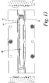
- FIG. 13 is a cross-sectional view of the window assembly of FIG. 11 taken along the line 13 — 13 .
- FIG. 1 shows an isometric, external view of a laser gain module 10 according to one embodiment of the present invention.
- the laser gain module 10 comprises a heat shield 12 including a first heat shield component 14 and a second heat shield component 16 .
- the structure and function of the heat shield 12 will be explained more fully below.
- the laser gain module 10 contains a solid-state laser slab 60 (as shown in FIG. 3 , below) which is optically pumped by diode arrays, also provided within the laser gain module 10 , in diode array assemblies 24 .
- the diode array assemblies 24 are held by diode mounts 18 , which support the diode array assemblies 24 and also allow for translation of the diodes toward and away from the solid-state laser slab 60 and for control over the angles at which light leaving the diode array assemblies 24 enters the solid-state laser slab 60 .
- the control of translation and angle of the diode mounts 18 allows for control and optimization of pump uniformity and optical path difference (OPD) uniformity.
- OPD optical path difference
- the diode mount 18 b shown in FIG. 1 , is held on the laser gain module 10 along a lower mount portion by spring-loaded bolts 20 driven into a gain module chassis 36 .
- the spring-loaded bolts 20 are loaded with compression springs 21 which exert an inward force on a lower lever portion 22 of the diode mount 18 .
- the direction of the force exerted on the lower lever portion 22 of the diode mount 18 by the compression springs 21 is shown by arrow “A” in FIG. 1 .
- Leverage on the diode mount 18 moves the diode array assembly 24 outwardly, in the direction shown by arrow “B” in FIG. 1 .
- the diode array assembly 24 is prevented from moving outwardly by a diode angle adjustment screw 26 provided within an adjustment bracket 28 , which in turn is mounted to a slab housing block 80 .
- the diode angle adjustment screw 26 presses against a diode adjustment support 32 which protrudes upwardly from the diode array assembly 24 through a slot provided within the adjustment bracket 28 .
- the diode adjustment support 32 is shown as a screw extending upwardly from the diode array assembly 24 , the diode adjustment support could be other devices as well, such as a pin, dowel, or platform secured to the diode array assembly 24 or otherwise adapted to move with the diode array assembly 24 .
- the first and second heat shield components 14 and 16 are mounted to a liquid-cooled heat shield base 34 provided on a gain module chassis 36 .
- An output beam aperture 37 is provided within the heat shield 12 for allowing an output beam to exit when the laser slab 60 converts pump energy to the output beam.
- First and second diode mounts 18 a and 18 b attach to opposite sides of the gain module chassis 36 , and the spring-loaded bolts 20 extend through apertures 38 provided within lever portions 22 of the diode mounts 18 a and 18 b .
- Outer mount shields 40 are mounted to the diode mounts 18 a and 18 b to contain the diode array assemblies 24 and to protect the diode array assemblies 24 from damage.
- Adjustment brackets 28 for facilitating adjustment of the diode angles relative to laser slab 60 are provided on the gain module chassis 36 .
- the gain module chassis 36 supports a slab housing 42 holding a solid-state laser slab 60 which is optically pumped by energy from energy emission regions 25 of the diodes within the diode array assemblies 24 .
- the laser slab 60 , the diode array assemblies 24 , and the surrounding support structure must be cooled due to the heat generated by the optical pumping process and by the generation of an output beam within the laser slab 60 .
- cooling is accomplished using a liquid cooling system, using liquid conduits provided in system components.
- FIG. 2 Several features of the laser gain module 10 related to cooling are shown in FIG. 2 , including a coolant entry 44 , a coolant outlet 46 , diode coolant conduit assemblies 48 (which include diode coolant conduits 50 , O-rings 52 , and diode coolant conduit brackets 54 and seal rings 56 ), and mount coolant ports 58 .
- the diode coolant conduit assemblies 48 allow for the provisioning of coolant to the diode array assemblies 24 even as the diode array assemblies 24 are angled and translated with respect to the laser slab 60 .
- the functions of the cooling-related components will be explained more completely below with respect to FIGS. 5–10 .
- FIG. 3 is an exploded view of the slab housing 42 .
- the slab housing 42 serves to hold a solid-state laser slab 60 , to direct coolant to and around the laser slab 60 , and to provide windows through which pump radiation is directed to the laser slab 60 .
- the laser slab 60 is supported between first and second edge bars 62 and 64 .
- the slab 60 is held in place along edge bar interfaces 118 (shown in FIG. 12 ). It is preferable to bond the slab to the edge bars 62 and 64 using a thermally conductive and somewhat elastomeric adhesive, such as boron-nitride filled silicone room-temperature-vulcanizing (RTV) adhesive.
- RTV room-temperature-vulcanizing
- the present invention may employ slabs made of any type of solid-state laser slab material, for example Nd:YAG. It is preferred to keep the laser slab 60 at a constant temperature, even when the laser gain device is not in operation.
- the edge bars 62 and 64 are electrically heated by current through first and second edge bar conductors 66 and 68 .
- the first and second edge bars 62 and 64 are held together by edge bar brackets 70 , which include coolant conduits to direct coolant from the chassis 36 , positioned below the laser slab 60 , through edge bar bracket apertures 72 into edge bar coolant apertures 74 , through the edge bars 62 and 64 , and then back down into the chassis 36 .
- the edge bar bracket apertures 72 and the edge bar coolant apertures 74 are sealed by O-rings 76 to prevent coolant leakage.
- Each of the slab housing blocks 78 and 80 contains a window 86 through which pump energy enters the laser slab 60 .
- pump energy shields 88 and 90 may be positioned between one or both windows 86 and the laser slab 60 to control pump energy entering the laser slab 60 .
- the laser slab 60 is sealed to each of the slab housing blocks 78 and 80 with slab seals 92 .
- the slab seals 92 allow the laser slab 60 to be liquid cooled.
- the slab seals 92 are preferably compressed between the housing blocks 78 and 80 and the laser slab 60 and in one embodiment are comprised of compressible material such as Viton® material made by DuPont, or silicone rubber material. According to one embodiment, the slab seals 92 are compressed to a width of approximately 0.6 inch, though greater or lesser compressions may be used depending on the choice of material. Any seal material compatible with the coolant may be used, and it is preferred to choose a material that experiences little to no degradation when exposed to laser light from the diode array assemblies 24 or generated within the laser slab 60 .
- FIG. 3 Also shown in FIG. 3 are mounting screws 94 for mounting the edge bar brackets 70 to the edge bars 62 and 64 and assembly pin nuts 96 for the assembly pins 82 to screw into.
- the diode adjustment bracket 28 opposes and is connected to a top assembly pin 82 .
- FIG. 4 a side view of a laser gain module 10 according to the present invention is shown.
- the outer mount shield 40 has been removed to provide a more direct view of the diode array assembly 24 .
- Diode electrical connectors 98 provide power to and allow control of pump radiation from the diode array assemblies 24 shown.
- FIG. 5 a cross-section along the line 5 — 5 of FIG. 4 is shown. This cross-sectional view more clearly shows the construction of the laser gain module 10 and illustrates the assembly of several components of the laser device.
- Cooling liquid conduits 100 are shown extending throughout several components of the laser gain module 10 , including the gain module chassis 36 and the diode mounts 18 .
- Heat shield conduits 102 extend through the heat shield base 34 and slab cooling conduits 104 are shown on opposing sides of the laser slab 60 , positioned between the laser slab 60 and the windows 86 .
- the diode coolant conduits 50 for directing coolant liquid between the gain module chassis 36 and the diode mounts 18 are also shown, along with O-rings 52 and seal rings 56 .
- the seal rings 56 ensure that coolant liquid does not leak when the diode mounts 18 are tilted or placed at different spacings within the laser gain module 10 .
- FIG. 5 illustrates the ability to control the angle of pump energy entering the laser slab 60 as well as translation of the diode array assemblies 24 toward and away from the laser slab 60 .
- the diode mounts 18 a and 18 b in the embodiment shown in FIG. 5 are provided with diode tilt fulcrums 106 .
- the lower lever portions 22 of the diode mounts 18 a and 18 b are biased inwardly toward the gain module chassis 36 , in the directions shown by the arrows “D” of FIG. 5 , a force will be exerted away from the gain module chassis 36 , in the directions shown by the arrows “E” of FIG. 5 , at the diode angle adjustment screws 26 .
- the diode angle adjustment screws 26 oppose the diode adjustment supports 32 , which are moved toward and away from the center of the gain module chassis 36 within adjustment support slots 110 .
- the angle of light emitted from the energy emission regions 25 of the diode array assemblies 24 may be adjusted downwardly, and by turning the diode angle adjustment screws 26 outwardly, the angle of light emitted by the energy emission regions 25 of the diode array assemblies 24 may be adjusted upwardly.
- the embodiment shown in FIG. 5 also allows for the distance from each of the diode array assemblies 24 to the laser slab 60 to be altered by the placement of diode spacers between one or both of the diode tilt fulcrums 106 and the first and second slab housing blocks 78 and 80 .
- the diode spacers are strips of stainless steel tape allowing the spacing of one or both of the diode mounts 18 in increments of the tape thickness.
- stainless steel tape having a thickness of approximately 0.005 inch is used for diode spacing.
- the diode array assemblies 24 may be translated toward or away from the laser slab 60 via the diode spacers or angled with respect to the laser slab 60 via the adjustment screws 26 to assure that a desirable amount of pump radiation is inserted into the laser slab 60 at desired angles. This assists in achieving a well-defined, homogeneously illuminated window for each side of the laser slab 60 . Further, diode array adjustment allows for the direction of pump radiation toward the laser slab 60 so as to compensate for thermal non-uniformities in the slab. While FIG. 5 shows a two-sided laser gain module 10 , it is to be understood that the principles of the present invention may, in an alternative embodiment, be directed to a laser gain module in which a laser slab is pumped from only one side.
- FIG. 6 a cross-sectional view of a laser gain module 10 along the line 6 — 6 of FIG. 4 is shown.
- This cross-sectional view further shows the cooling liquid conduits 100 extending through the laser gain module 10 .
- This view also shows an assembly pin 82 extending through the first and second slab housing blocks 78 and 80 and also extending through a laser slab spacer 84 , which keeps the slab housing blocks 78 and 80 spaced at an optimum distance for the laser slab 60 .
- the laser slab spacer 84 is approximately twice the width of the laser slab 60 .
- the present invention contemplates laser slab spacers 84 having a range of widths, with specific widths chosen based on the width of the laser slab 60 and the desired spacing of the slab housing blocks 78 and 80 .
- Cooling liquid conduits 100 in the diode mounts 18 can also be seen in this view.
- First and second edge bars 62 and 64 are shown holding the laser slab 60 from the top and bottom, respectively.
- the laser slab spacers 84 are approximately the width of the laser slab 60 and they keep the first and second slab housing blocks 78 and 80 an appropriate distance from the laser slab 60 , preventing the slab housing blocks 78 and 80 from contacting the laser slab 60 .
- changeable laser slab spacers 84 allows for the adjustment of spacing between the slab housing blocks 78 and 80 for particular laser slabs, or for a single laser slab whose thickness changes over time.
- the laser slab spacers 84 are made of stainless steel, but other materials such as ceramics, plastics, and other metals may be used. It is preferred to construct the laser slab spacers 84 of materials that have thermal expansion characteristics similar to the thermal expansion characteristics of the assembly pins 82 to minimize thermal expansion problems.
- Laser slab thicknesses may change as a result of polishing or of work done on the laser slab to remove flaws on the laser slab surface.
- the laser slab spacers 84 allow the re-use of remaining laser gain module components, reducing or eliminating the need for remanufacturing or customization of other laser gain module components.
- the laser slab spacers 84 also allow for optimization of seals around differently-sized laser slabs 60 , preventing or reducing leaking of coolant from the area of a narrower slab and preventing or reducing the overcompression of seals surrounding larger slabs. Overcompression of seals can lead to slab damage and damage to hardware surrounding the slab.
- FIG. 7 shows a cross-sectional view of a laser gain module 10 along the line 7 — 7 of FIG. 4 .
- Cooling liquid conduits 100 in the first and second slab housing blocks 78 and 80 transport cooling liquid to and from the heat shield base 34 (shown in FIG. 2 ) as explained more fully below. Cooling liquid conduits 100 can also be seen extending through the diode array assemblies 24 .
- the first and second slab housing blocks 78 and 80 are provided with slab cooling liquid diverters 112 for diverting cooling liquid through the slab cooling conduits 104 and thereby to directly cool the laser slab 60 .
- cooling liquid is diverted to the laser slab 60 at a ratio of approximately 8:1 in comparison to the diversion of cooling liquid to the heat shield base 34 .
- cooling liquid for example, if approximately eight gallons per minute of cooling liquid are directed to the slab cooling conduits 104 for cooling the laser slab 60 , then approximately one gallon per minute of cooling liquid will be directed to the heat shield base 34 . Greater or lesser diversion ratios may be used to achieve efficient cooling of the laser slab 60 and surrounding components.
- FIG. 8 an isometric view of an assembled laser gain module 10 is shown with heat shield components 14 and 16 , outer mount shields 40 , and diode mounts 18 removed to give a more complete exterior view of an assembled gain module.
- the window 86 within the second slab housing block 80 allows pump radiation from the diode array assemblies 24 (not shown in FIG. 8 ) to enter the laser slab 60 (positioned behind the window 80 of FIG. 8 ).
- Edge bar conductors 66 and 68 extend from the edge bars 62 and 64 (not shown in FIG. 8 ) into an edge bar current input 114 which allows for the heating of the edge bars 62 and 64 and the maintenance of the edge bars 62 and 64 at a proper temperature.
- Cooling liquid conduits 100 are provided within the gain module chassis 36 , and table mounts 116 are provided for mounting the gain module chassis 36 to a stable platform.
- FIG. 9 A front view of the laser gain module 10 with heat shield components 14 and 16 , outer mount shields 40 , and diode mounts 18 removed is shown in FIG. 9 , and a cross-sectional view along the line 10 — 10 of the laser gain module 10 with these shields and diode array mounts removed is shown in FIG. 10 .
- Cooling liquid conduits 100 provided in the gain module chassis 36 carry cooling liquid upwardly to the cooling liquid conduits 100 within the slab housing blocks 78 and 80 .
- Cooling liquid diverters 112 divert cooling liquid to the laser slab 60 .
- O-rings 76 are provided at the interfaces of the gain module chassis 36 and the slab housing blocks 78 and 80 and also at the interfaces of the heat shield base 34 and the slab housing blocks 78 and 80 .
- coolant liquid is directed through the laser gain module 10 and used to cool a heat shield 12 , as shown in FIGS. 1 and 2 .
- the heat shield 12 serves to contain non-lasing radiation within the laser gain module 10 , absorbing non-lasing radiation and protecting surrounding components from the non-lasing radiation.
- Coolant liquid such as purified water, enters the gain module chassis 36 through a coolant entry 44 and exits the gain module chassis 36 through a coolant outlet 46 as shown in FIG. 2 .
- Coolant enters and exits the diode mount 18 b through a diode coolant conduit assembly 48 , which includes diode coolant conduits 50 contacting the gain module chassis 36 at O-rings 52 .
- a diode coolant conduit bracket 54 supports the coolant conduits 50 and provides for spacing between the diode mount 18 b and the gain module chassis 36 .
- the coolant conduits 50 are provided with seal rings 56 to prevent leakage of coolant from mount coolant ports 58 when the diode angles are adjusted as described above.
- the gain module chassis 36 includes cooling liquid conduits which direct coolant upwardly through the slab housing 42 and to the heat shield base 34 . The coolant then flows downwardly through the slab housing 42 to the coolant outlet 46 .
- cooling liquid conduits 100 are provided within the slab housing blocks 78 and 80 to direct coolant upwardly to the heat shield base 34 .
- Heat shield coolant conduits 102 as shown in FIGS.
- the heat shield base 34 conductively cools the heat shield components 14 and 16 and keeps them at a safe operating temperature, thereby protecting the surrounding environment from unwanted temperature increases.
- the heat shield 12 may be provided with angled or curved portions to absorb stray radiation in the laser gain module 10 .
- FIG. 11 A side view of the laser slab housing blocks 78 and 80 is shown in FIG. 11 .
- An edge bar bracket 70 is shown for holding the edge bars 62 and 64 (not shown in FIG. 1 ) between the slab housing blocks 78 and 80 , and the edge bar conductors 66 and 68 extend behind the edge bar bracket and toward the edge bars 62 and 64 .
- a cross-sectional view of the assembly along the line 12 — 12 is shown in FIG. 12 .
- the laser slab 60 is shown mounted between the first and second edge bars 62 and 64 and held between edge bar slab interfaces 118 .
- Cooling liquid conduits 100 extend through the edge bar brackets 70 and through the first and second edge bars 62 and 64 .
- Laser slab spacers 84 are also shown in FIG. 12 , with one laser slab spacer 84 shown in the first edge bar 62 and two laser slab spacers 84 shown in the second edge bar 64 .
- FIG. 13 a cross-sectional view along the line 13 — 13 of FIG. 11 shows the window 86 with a surrounding slab seal 92 .
- Upper and lower pump energy shields 88 and 90 are provided on the window 86 . While the embodiment of FIG. 13 shows both upper and lower pump energy shields 88 and 90 , it is to be understood that only one of the two shields may be provided in some embodiments.
- the pump energy shields 88 and 90 are provided to control the amount of pump energy entering the laser slab 60 , and the location of the laser slab 60 through which pump energy is input into the laser slab 60 .
- upper pump energy shields 88 and lower pump energy shields 90 are provided so that not all optical energy entering through the windows 86 necessarily enters the laser slab 60 .
- the pump energy shields 88 and 90 define an aperture for controlling the amount and direction of pump energy that enters the laser slab 60 .
- the pump energy shields 88 and 90 are provided to keep optical pump energy within an ideal energy input area of the laser slab 60 .
- One benefit of vertical isotherms is better uniformity of the refractive index throughout the laser slab 60 .
- the laser slab 60 is heated to a greater temperature in locations excited by pump energy. Thus, if pump energy is concentrated toward the center of the laser slab 60 , the center of the laser slab 60 will heat up and the edges of the laser slab 60 will stay at a relatively cooler temperature.
- the pump energy shields 88 and 90 may be properly sized and spaced apart to maximize efficient optical pumping of the laser slab 60 . According to some embodiments, the pump energy shields 88 and 90 serve to compensate for manufacturing differences in pumping diode arrays.
- the pump energy shields 88 and 90 are positioned and sized to shield less than approximately 5% of the surface area of each of the windows 86 .
- the pump energy shields 88 and 90 can comprise stainless steel tape with an acrylic-based adhesive adhering the pump energy shields 88 and 90 to the windows 86 .
- the pump energy shields 88 and 90 may comprise other materials such as ceramic or copper shielding.
Landscapes
- Physics & Mathematics (AREA)
- Electromagnetism (AREA)
- Engineering & Computer Science (AREA)
- Plasma & Fusion (AREA)
- Optics & Photonics (AREA)
- Chemical & Material Sciences (AREA)
- Crystallography & Structural Chemistry (AREA)
- Lasers (AREA)
- Semiconductor Lasers (AREA)
Abstract
A laser gain device (10) holds a laser slab (60) which is pumped by pump energy from at least one diode array assembly (24). An angle at which pump energy from the diode array assembly (24) impinges the laser slab (60) is adjustable via angle adjustment means. The laser slab (60) is mounted between edge bars (62, 64) which have laser slab spacers (84) extending therethrough, allowing laser slabs (60) of different widths to be mounted within the laser gain device (10). One or more pump energy shields (88, 90) are used to control the amount of pump energy entering the laser slab (60), and cooling liquid conduits (100) are provided throughout components of the laser gain device (10), serving to conductively cool a heat shield (12).
Description
1. Field of the Invention
The present invention relates generally to optical components and more specifically relates to a diode-pumped laser gain module.
2. Description of the Prior Art
Laser gain devices employing laser slabs use sources of optical energy to pump laser slabs and produce an output laser beam. Output beams may be used in applications such as optical lithography for microchip production.
While laser gain devices have achieved success and are widely used, they have some shortcomings. For example, many laser gain devices are sized for use with a certain type of laser slab having specific dimensions, and even laser slabs designed to have the same dimensions may have slight variations that impact their exact fit into a laser device. The choice of a different laser slab—or the replacement of a worn or damaged laser slab with a new laser slab—may require reconstruction of several parts of a laser system to accommodate a laser slab of a different size.
Further, it is desirable to maximize the amount of input optical energy (for example, from one or more diode arrays) entering the optimum area of a laser slab. Removal of a laser slab from a laser gain device for repair or replacement may change the alignment or the amount of optical energy entering the laser slab, thereby decreasing the overall efficiency of the system.
The considerations of proper direction of input energy and optimization of the laser device to accommodate specific laser slab sizes impact the heat dissipation of the laser device. As changes are made to the laser device for the purposes of fitting laser slabs and optimizing light input into laser slabs, the efficiency of heat removal from the laser device may change.
There is a need for a laser gain module that allows for optimization of the gain module for different laser slabs, control of the amount and angle of light entering a laser slab, and efficient heat dissipation from within the gain module.
These and other goals are achieved by embodiments of the present invention.
According to one embodiment of the present invention, a laser gain module comprises top and bottom edge bars contacting the laser slab and having variable spacers for accommodating different slab sizes.
According to another embodiment of the present invention, a laser gain module is provided with one or more adjustable diode array brackets for changing the distance between diode arrays and a laser slab and also for changing the angle of diode light as it enters a laser slab.
According to a further embodiment of the present invention, changeable light shields are provided within a laser gain module between a window and a laser slab for allowing control of the amount and location of light entering a laser slab.
According to still another embodiment of the present invention, a conductively cooled heat shield is provided for allowing easy removal of a heat shield device and efficient use of cooling fluid in a laser gain module.
The above summary of the present invention is not intended to represent each embodiment or every aspect of the present invention. This is the purpose of the Figures and the detailed description which follows.
The foregoing and other advantages of the invention will become apparent upon reading the following detailed description and upon reference to the drawings.
While the invention is susceptible to various modifications and alternative forms, specific embodiments have been shown by way of example in the drawings and will be described in detail herein. It should be understood, however, that the invention is not intended to be limited to the particular forms disclosed. Rather, the invention is to cover all modifications, equivalents, and alternatives falling within the spirit and scope of the invention as defined by the appended claims.
Turning now to the drawings, FIG. 1 shows an isometric, external view of a laser gain module 10 according to one embodiment of the present invention. The laser gain module 10 comprises a heat shield 12 including a first heat shield component 14 and a second heat shield component 16. The structure and function of the heat shield 12 will be explained more fully below. The laser gain module 10 contains a solid-state laser slab 60 (as shown in FIG. 3 , below) which is optically pumped by diode arrays, also provided within the laser gain module 10, in diode array assemblies 24. The diode array assemblies 24, in turn, are held by diode mounts 18, which support the diode array assemblies 24 and also allow for translation of the diodes toward and away from the solid-state laser slab 60 and for control over the angles at which light leaving the diode array assemblies 24 enters the solid-state laser slab 60. According to one embodiment, the control of translation and angle of the diode mounts 18 allows for control and optimization of pump uniformity and optical path difference (OPD) uniformity.
The diode mount 18 b, shown in FIG. 1 , is held on the laser gain module 10 along a lower mount portion by spring-loaded bolts 20 driven into a gain module chassis 36. The spring-loaded bolts 20 are loaded with compression springs 21 which exert an inward force on a lower lever portion 22 of the diode mount 18. The direction of the force exerted on the lower lever portion 22 of the diode mount 18 by the compression springs 21 is shown by arrow “A” in FIG. 1 . Leverage on the diode mount 18, as described more completely below with respect to FIG. 5 , moves the diode array assembly 24 outwardly, in the direction shown by arrow “B” in FIG. 1 . The diode array assembly 24 is prevented from moving outwardly by a diode angle adjustment screw 26 provided within an adjustment bracket 28, which in turn is mounted to a slab housing block 80. The diode angle adjustment screw 26 presses against a diode adjustment support 32 which protrudes upwardly from the diode array assembly 24 through a slot provided within the adjustment bracket 28. While the diode adjustment support 32 is shown as a screw extending upwardly from the diode array assembly 24, the diode adjustment support could be other devices as well, such as a pin, dowel, or platform secured to the diode array assembly 24 or otherwise adapted to move with the diode array assembly 24.
The first and second heat shield components 14 and 16 are mounted to a liquid-cooled heat shield base 34 provided on a gain module chassis 36. An output beam aperture 37 is provided within the heat shield 12 for allowing an output beam to exit when the laser slab 60 converts pump energy to the output beam.
Turning now to FIG. 2 , the heat shield components 14 and 16 are shown elevated over the heat shield base 34 to which they are mounted. First and second diode mounts 18 a and 18 b attach to opposite sides of the gain module chassis 36, and the spring-loaded bolts 20 extend through apertures 38 provided within lever portions 22 of the diode mounts 18 a and 18 b. Outer mount shields 40 are mounted to the diode mounts 18 a and 18 b to contain the diode array assemblies 24 and to protect the diode array assemblies 24 from damage. Adjustment brackets 28 for facilitating adjustment of the diode angles relative to laser slab 60 are provided on the gain module chassis 36.
The gain module chassis 36 supports a slab housing 42 holding a solid-state laser slab 60 which is optically pumped by energy from energy emission regions 25 of the diodes within the diode array assemblies 24. The laser slab 60, the diode array assemblies 24, and the surrounding support structure must be cooled due to the heat generated by the optical pumping process and by the generation of an output beam within the laser slab 60. As will be described more completely below, cooling is accomplished using a liquid cooling system, using liquid conduits provided in system components.
Several features of the laser gain module 10 related to cooling are shown in FIG. 2 , including a coolant entry 44, a coolant outlet 46, diode coolant conduit assemblies 48 (which include diode coolant conduits 50, O-rings 52, and diode coolant conduit brackets 54 and seal rings 56), and mount coolant ports 58. The diode coolant conduit assemblies 48 allow for the provisioning of coolant to the diode array assemblies 24 even as the diode array assemblies 24 are angled and translated with respect to the laser slab 60. The functions of the cooling-related components will be explained more completely below with respect to FIGS. 5–10 .
Each of the slab housing blocks 78 and 80 contains a window 86 through which pump energy enters the laser slab 60. As described in greater detail below, pump energy shields 88 and 90 may be positioned between one or both windows 86 and the laser slab 60 to control pump energy entering the laser slab 60.
The laser slab 60 is sealed to each of the slab housing blocks 78 and 80 with slab seals 92. The slab seals 92 allow the laser slab 60 to be liquid cooled. The slab seals 92 are preferably compressed between the housing blocks 78 and 80 and the laser slab 60 and in one embodiment are comprised of compressible material such as Viton® material made by DuPont, or silicone rubber material. According to one embodiment, the slab seals 92 are compressed to a width of approximately 0.6 inch, though greater or lesser compressions may be used depending on the choice of material. Any seal material compatible with the coolant may be used, and it is preferred to choose a material that experiences little to no degradation when exposed to laser light from the diode array assemblies 24 or generated within the laser slab 60.
Also shown in FIG. 3 are mounting screws 94 for mounting the edge bar brackets 70 to the edge bars 62 and 64 and assembly pin nuts 96 for the assembly pins 82 to screw into. In the embodiment shown in FIG. 3 , the diode adjustment bracket 28 opposes and is connected to a top assembly pin 82.
Turning now to FIG. 4 , a side view of a laser gain module 10 according to the present invention is shown. In the side view of FIG. 4 , the outer mount shield 40, has been removed to provide a more direct view of the diode array assembly 24. Diode electrical connectors 98 provide power to and allow control of pump radiation from the diode array assemblies 24 shown.
Turning now to FIG. 5 , a cross-section along the line 5—5 of FIG. 4 is shown. This cross-sectional view more clearly shows the construction of the laser gain module 10 and illustrates the assembly of several components of the laser device.
Cooling liquid conduits 100 are shown extending throughout several components of the laser gain module 10, including the gain module chassis 36 and the diode mounts 18. Heat shield conduits 102 extend through the heat shield base 34 and slab cooling conduits 104 are shown on opposing sides of the laser slab 60, positioned between the laser slab 60 and the windows 86. The diode coolant conduits 50 for directing coolant liquid between the gain module chassis 36 and the diode mounts 18 are also shown, along with O-rings 52 and seal rings 56. The seal rings 56 ensure that coolant liquid does not leak when the diode mounts 18 are tilted or placed at different spacings within the laser gain module 10.
The embodiment shown in FIG. 5 also allows for the distance from each of the diode array assemblies 24 to the laser slab 60 to be altered by the placement of diode spacers between one or both of the diode tilt fulcrums 106 and the first and second slab housing blocks 78 and 80. In one embodiment, the diode spacers are strips of stainless steel tape allowing the spacing of one or both of the diode mounts 18 in increments of the tape thickness. According to one embodiment, stainless steel tape having a thickness of approximately 0.005 inch is used for diode spacing. Thus the diode array assemblies 24 may be translated toward or away from the laser slab 60 via the diode spacers or angled with respect to the laser slab 60 via the adjustment screws 26 to assure that a desirable amount of pump radiation is inserted into the laser slab 60 at desired angles. This assists in achieving a well-defined, homogeneously illuminated window for each side of the laser slab 60. Further, diode array adjustment allows for the direction of pump radiation toward the laser slab 60 so as to compensate for thermal non-uniformities in the slab. While FIG. 5 shows a two-sided laser gain module 10, it is to be understood that the principles of the present invention may, in an alternative embodiment, be directed to a laser gain module in which a laser slab is pumped from only one side.
Turning now to FIG. 6 , a cross-sectional view of a laser gain module 10 along the line 6—6 of FIG. 4 is shown. This cross-sectional view further shows the cooling liquid conduits 100 extending through the laser gain module 10. This view also shows an assembly pin 82 extending through the first and second slab housing blocks 78 and 80 and also extending through a laser slab spacer 84, which keeps the slab housing blocks 78 and 80 spaced at an optimum distance for the laser slab 60. In the embodiment shown in FIG. 6 , the laser slab spacer 84 is approximately twice the width of the laser slab 60. The present invention contemplates laser slab spacers 84 having a range of widths, with specific widths chosen based on the width of the laser slab 60 and the desired spacing of the slab housing blocks 78 and 80. Cooling liquid conduits 100 in the diode mounts 18 can also be seen in this view. First and second edge bars 62 and 64 are shown holding the laser slab 60 from the top and bottom, respectively.
According to one embodiment, the laser slab spacers 84 are approximately the width of the laser slab 60 and they keep the first and second slab housing blocks 78 and 80 an appropriate distance from the laser slab 60, preventing the slab housing blocks 78 and 80 from contacting the laser slab 60.
The use of changeable laser slab spacers 84 allows for the adjustment of spacing between the slab housing blocks 78 and 80 for particular laser slabs, or for a single laser slab whose thickness changes over time. According to one embodiment, the laser slab spacers 84 are made of stainless steel, but other materials such as ceramics, plastics, and other metals may be used. It is preferred to construct the laser slab spacers 84 of materials that have thermal expansion characteristics similar to the thermal expansion characteristics of the assembly pins 82 to minimize thermal expansion problems.
Laser slab thicknesses may change as a result of polishing or of work done on the laser slab to remove flaws on the laser slab surface. When laser slabs 60 having different thicknesses are used in the laser gain module 10, the laser slab spacers 84 allow the re-use of remaining laser gain module components, reducing or eliminating the need for remanufacturing or customization of other laser gain module components. The laser slab spacers 84 also allow for optimization of seals around differently-sized laser slabs 60, preventing or reducing leaking of coolant from the area of a narrower slab and preventing or reducing the overcompression of seals surrounding larger slabs. Overcompression of seals can lead to slab damage and damage to hardware surrounding the slab.
Turning now to FIG. 8 , an isometric view of an assembled laser gain module 10 is shown with heat shield components 14 and 16, outer mount shields 40, and diode mounts 18 removed to give a more complete exterior view of an assembled gain module. The window 86 within the second slab housing block 80 allows pump radiation from the diode array assemblies 24 (not shown in FIG. 8 ) to enter the laser slab 60 (positioned behind the window 80 of FIG. 8 ). Edge bar conductors 66 and 68 extend from the edge bars 62 and 64 (not shown in FIG. 8 ) into an edge bar current input 114 which allows for the heating of the edge bars 62 and 64 and the maintenance of the edge bars 62 and 64 at a proper temperature.
Also visible in FIG. 8 are the coolant entry 44 and the coolant outlet 46 of the gain module chassis 36. Cooling liquid conduits 100 are provided within the gain module chassis 36, and table mounts 116 are provided for mounting the gain module chassis 36 to a stable platform.
A front view of the laser gain module 10 with heat shield components 14 and 16, outer mount shields 40, and diode mounts 18 removed is shown in FIG. 9 , and a cross-sectional view along the line 10—10 of the laser gain module 10 with these shields and diode array mounts removed is shown in FIG. 10 . Cooling liquid conduits 100 provided in the gain module chassis 36 carry cooling liquid upwardly to the cooling liquid conduits 100 within the slab housing blocks 78 and 80. Cooling liquid diverters 112 divert cooling liquid to the laser slab 60. O-rings 76 are provided at the interfaces of the gain module chassis 36 and the slab housing blocks 78 and 80 and also at the interfaces of the heat shield base 34 and the slab housing blocks 78 and 80.
According to one embodiment of the present invention, coolant liquid is directed through the laser gain module 10 and used to cool a heat shield 12, as shown in FIGS. 1 and 2 . The heat shield 12 serves to contain non-lasing radiation within the laser gain module 10, absorbing non-lasing radiation and protecting surrounding components from the non-lasing radiation. Coolant liquid, such as purified water, enters the gain module chassis 36 through a coolant entry 44 and exits the gain module chassis 36 through a coolant outlet 46 as shown in FIG. 2 . Coolant enters and exits the diode mount 18 b through a diode coolant conduit assembly 48, which includes diode coolant conduits 50 contacting the gain module chassis 36 at O-rings 52. A diode coolant conduit bracket 54 supports the coolant conduits 50 and provides for spacing between the diode mount 18 b and the gain module chassis 36. The coolant conduits 50 are provided with seal rings 56 to prevent leakage of coolant from mount coolant ports 58 when the diode angles are adjusted as described above. The gain module chassis 36 includes cooling liquid conduits which direct coolant upwardly through the slab housing 42 and to the heat shield base 34. The coolant then flows downwardly through the slab housing 42 to the coolant outlet 46. As shown in FIGS. 3 , 7, and 10, cooling liquid conduits 100 are provided within the slab housing blocks 78 and 80 to direct coolant upwardly to the heat shield base 34. Heat shield coolant conduits 102, as shown in FIGS. 5 , 6, and 10 run through the heat shield base 34. Thus, as the heat shield components 14 and 16 are heated by the absorption of non-lasing radiation, the heat shield base 34 conductively cools the heat shield components 14 and 16 and keeps them at a safe operating temperature, thereby protecting the surrounding environment from unwanted temperature increases. As shown in FIGS. 1 and 2 , the heat shield 12 may be provided with angled or curved portions to absorb stray radiation in the laser gain module 10.
A side view of the laser slab housing blocks 78 and 80 is shown in FIG. 11 . An edge bar bracket 70 is shown for holding the edge bars 62 and 64 (not shown in FIG. 1 ) between the slab housing blocks 78 and 80, and the edge bar conductors 66 and 68 extend behind the edge bar bracket and toward the edge bars 62 and 64. A cross-sectional view of the assembly along the line 12—12 is shown in FIG. 12 .
In FIG. 12 , the laser slab 60 is shown mounted between the first and second edge bars 62 and 64 and held between edge bar slab interfaces 118. Cooling liquid conduits 100 extend through the edge bar brackets 70 and through the first and second edge bars 62 and 64. Laser slab spacers 84 are also shown in FIG. 12 , with one laser slab spacer 84 shown in the first edge bar 62 and two laser slab spacers 84 shown in the second edge bar 64.
Turning now to FIG. 13 , a cross-sectional view along the line 13—13 of FIG. 11 shows the window 86 with a surrounding slab seal 92. Upper and lower pump energy shields 88 and 90 are provided on the window 86. While the embodiment of FIG. 13 shows both upper and lower pump energy shields 88 and 90, it is to be understood that only one of the two shields may be provided in some embodiments. The pump energy shields 88 and 90 are provided to control the amount of pump energy entering the laser slab 60, and the location of the laser slab 60 through which pump energy is input into the laser slab 60. To control the vertical location on the laser slab 60 at which pump energy is allowed to enter the laser slab 60, upper pump energy shields 88 and lower pump energy shields 90 are provided so that not all optical energy entering through the windows 86 necessarily enters the laser slab 60. Thus, the pump energy shields 88 and 90 define an aperture for controlling the amount and direction of pump energy that enters the laser slab 60.
According to one embodiment, the pump energy shields 88 and 90 are provided to keep optical pump energy within an ideal energy input area of the laser slab 60. For efficient and reliable laser operation, it is desirable to keep isotherms within the laser slab 60 running vertically (in the direction of arrow C of FIGS. 3 and 12 ) through the laser slab 60. One benefit of vertical isotherms is better uniformity of the refractive index throughout the laser slab 60. The laser slab 60 is heated to a greater temperature in locations excited by pump energy. Thus, if pump energy is concentrated toward the center of the laser slab 60, the center of the laser slab 60 will heat up and the edges of the laser slab 60 will stay at a relatively cooler temperature. Similarly, if pump energy is allowed to approach the edges of the laser slab 60, the edges of the laser slab 60 will increase in temperature. The pump energy shields 88 and 90 may be properly sized and spaced apart to maximize efficient optical pumping of the laser slab 60. According to some embodiments, the pump energy shields 88 and 90 serve to compensate for manufacturing differences in pumping diode arrays.
In one preferred embodiment, the pump energy shields 88 and 90 are positioned and sized to shield less than approximately 5% of the surface area of each of the windows 86. The pump energy shields 88 and 90 can comprise stainless steel tape with an acrylic-based adhesive adhering the pump energy shields 88 and 90 to the windows 86. In alternative embodiments, the pump energy shields 88 and 90 may comprise other materials such as ceramic or copper shielding.
While the present invention has been described with reference to one or more particular embodiments, those skilled in the art will recognize that many changes may be made thereto without departing from the spirit and scope of the present invention. For example, while the diode mounts 18 have been described as having fluid flowing therein it is to be understood that diode mounts may be provided without fluid conduits and used primarily as supports for the diode array assemblies 24. Each of these embodiments and obvious variations thereof is contemplated as falling within the spirit and scope of the claimed invention, which is set forth in the following claims.
Claims (17)
1. A laser slab housing comprising:
first and second slab housing members defining a space therebetween for accepting laser slabs of differing dimensions, said first and second slab housing members being separated by a slab housing-gap dimension and each of said first and second slab housing members being separated from said laser slab by respective first and second slab distances;
a laser slab within said space between said first and second slab housing members, said laser slab having a slab dimension; and
one or more laser slab spacers between said first and second slab housing members, lengths of said laser slab spacers defining said slab housing-gap dimension, said one or more slab spacers being replaceable with laser slab spacers having different lengths such that said slab housing-gap dimension is alterable and at least one of said first and second slab distances remains approximately constant when said slab dimension is changed due to a change in laser slabs.
2. The laser slab housing of claim 1 further comprising at least one slab seal adapted to be compressed to a compression width between one of said first and second slab housing members and said laser slab.
3. The laser slab housing of claim 2 wherein said lengths of said laser slab spacers are chosen to maintain said compression width of said slab seal approximately constant when said laser slab is replaced with a differently-sized laser slab.
4. The laser slab housing of claim 1 in combination with a kit of laser slab spacers having laser slab spacers of different lengths, wherein said laser slab spacers are selected from said kit of laser slab spacers.
5. The laser slab housing of claim 1 wherein said one or more laser slab spacers have apertures therein for accepting assembly pins holding said first and second slab housing members together.
6. The laser slab housing of claim 1 wherein said one or more laser slab spacers are comprised of the same material as said slab housing members.
7. The laser slab housing of claim 1 wherein said laser slab is held between said first and second slab housing members by at least one edge bar, said at least one edge bar being adapted to accept at least one of said slab spacers therethrough.
8. A method for mounting laser slabs of different dimensions comprising:
providing first and second slab housing members spaced from one another by a slab housing-gap dimension and defining a slab-receiving space therebetween;
selecting at least one laser slab spacer from a plurality of laser slab spacers having a plurality of laser slab spacer lengths to provide a desired slab housing-gap dimension; and
spacing said first and second slab housings members from one another with said selected one or more of said laser slab spacers to accommodate said laser slab.
9. The method of claim 8 wherein said selecting includes choosing a longer slab spacer to increase said slab housing-gap dimension when laser slabs having a wider dimension are held within said slab-receiving space.
10. The method of claim 8 further comprising compressing at least one slab seal between a laser slab and at least one of said first and second slab housing members to a compression distance.
11. The method of claim 10 further comprising maintaining said compression distance for laser slabs having different dimensions by selecting and inserting slab spacers of appropriate slab spacer lengths between said first and second slab housing members.
12. The method of claim 10 further comprising mounting a laser slab in said slab receiving space between first and second edge bars.
13. The method of claim 8 further comprising adjusting said slab housing-gap dimension by replacing said laser slab spacers with laser slab spacers having different laser slab spacer lengths.
14. The method of claim 8 further comprising holding said first and second slab housing members together with assembly pins inserted through apertures provided within said laser slab spacers.
15. The method of claim 8 , further comprising maintaining approximately constant, when said slab housing-gap dimension is changed, at least one of respective distances between said first and second slab housing members and a laser slab of said laser slabs of different dimensions.
16. A method for mounting laser slabs of different dimensions comprising:
providing a housing assembly having a first slab located in a space defined by a first housing member and a second housing member, said first housing member and said second housing member being separated by a housing-gap dimension that is defined by a first spacer;
disassembling said housing assembly to remove said first slab from said space;
inserting a second slab in said space
replacing said first spacer with a second spacer such that said housing-gap dimension accommodates a difference between a first width of said first slab and a second width of said second slab; and
reassembling said housing assembly with said second slab and said second spacer.
17. The method of claim 16 , wherein said second spacer is selected such that said housing-gap dimension remains approximately constant.
Priority Applications (3)
| Application Number | Priority Date | Filing Date | Title |
|---|---|---|---|
| US10/602,057 US7170919B2 (en) | 2003-06-23 | 2003-06-23 | Diode-pumped solid-state laser gain module |
| JP2003381039A JP2005019940A (en) | 2003-06-23 | 2003-11-11 | Laser gain module and method for adjusting pump energy entering laser slab |
| EP03026059A EP1492207A3 (en) | 2003-06-23 | 2003-11-12 | Diode-pumped solid-state laser gain module |
Applications Claiming Priority (1)
| Application Number | Priority Date | Filing Date | Title |
|---|---|---|---|
| US10/602,057 US7170919B2 (en) | 2003-06-23 | 2003-06-23 | Diode-pumped solid-state laser gain module |
Publications (2)
| Publication Number | Publication Date |
|---|---|
| US20040258123A1 US20040258123A1 (en) | 2004-12-23 |
| US7170919B2 true US7170919B2 (en) | 2007-01-30 |
Family
ID=33418616
Family Applications (1)
| Application Number | Title | Priority Date | Filing Date |
|---|---|---|---|
| US10/602,057 Expired - Fee Related US7170919B2 (en) | 2003-06-23 | 2003-06-23 | Diode-pumped solid-state laser gain module |
Country Status (3)
| Country | Link |
|---|---|
| US (1) | US7170919B2 (en) |
| EP (1) | EP1492207A3 (en) |
| JP (1) | JP2005019940A (en) |
Cited By (4)
| Publication number | Priority date | Publication date | Assignee | Title |
|---|---|---|---|---|
| US20100008389A1 (en) * | 2008-07-14 | 2010-01-14 | Jackson Paul E | Inverted composite slab sandwich laser gain medium |
| WO2013033265A1 (en) * | 2011-08-29 | 2013-03-07 | Intellectual Light, Inc. | Mount for semiconductor devices using conformable conductive layers, and method |
| US9601904B1 (en) | 2015-12-07 | 2017-03-21 | Raytheon Company | Laser diode driver with variable input voltage and variable diode string voltage |
| US10903618B2 (en) * | 2019-03-20 | 2021-01-26 | Chroma Ate Inc. | Fixture assembly for testing edge-emitting laser diodes and testing apparatus having the same |
Families Citing this family (18)
| Publication number | Priority date | Publication date | Assignee | Title |
|---|---|---|---|---|
| ATE363753T1 (en) * | 2004-05-29 | 2007-06-15 | Trumpf Laser Gmbh & Co Kg | FASTENING ARRANGEMENT FOR A PUMP MODULE |
| CA2621629A1 (en) * | 2005-09-07 | 2007-03-15 | Ellex Medical Pty Ltd | Optical mount for laser rod |
| US7433376B1 (en) * | 2006-08-07 | 2008-10-07 | Textron Systems Corporation | Zig-zag laser with improved liquid cooling |
| CN103308481B (en) * | 2013-05-10 | 2015-06-03 | 北京理工大学 | Device for measuring optical performance of material under strong laser condition |
| CN104953446A (en) * | 2014-03-28 | 2015-09-30 | 中国科学院大连化学物理研究所 | Novel diode-pumping immersion-type liquid-cooling solid laser gain pool |
| KR101806894B1 (en) * | 2015-10-23 | 2017-12-08 | 국방과학연구소 | Air cooling type laser diode pumped chamber |
| US10211590B2 (en) * | 2015-11-25 | 2019-02-19 | Raytheon Company | Dual-function optical bench and cooling manifold for high-power laser system |
| US11114813B2 (en) | 2015-11-25 | 2021-09-07 | Raytheon Company | Integrated pumplight homogenizer and signal injector for high-power laser system |
| US10297968B2 (en) * | 2015-11-25 | 2019-05-21 | Raytheon Company | High-gain single planar waveguide (PWG) amplifier laser system |
| US9865988B2 (en) * | 2015-11-25 | 2018-01-09 | Raytheon Company | High-power planar waveguide (PWG) pumphead with modular components for high-power laser system |
| US10069270B2 (en) | 2016-02-11 | 2018-09-04 | Raytheon Company | Planar waveguides with enhanced support and/or cooling features for high-power laser systems |
| FR3049122B1 (en) * | 2016-03-21 | 2018-07-06 | Commissariat A L'energie Atomique Et Aux Energies Alternatives | LASER AMPLIFICATION DEVICE WITH ACTIVE BEAM QUALITY CONTROL |
| US9742142B1 (en) | 2016-05-04 | 2017-08-22 | Raytheon Company | Heat exchangers with tapered light scrapers for high-power laser systems and other systems |
| US10511135B2 (en) | 2017-12-19 | 2019-12-17 | Raytheon Company | Laser system with mechanically-robust monolithic fused planar waveguide (PWG) structure |
| US11133639B2 (en) | 2018-07-24 | 2021-09-28 | Raytheon Company | Fast axis thermal lens compensation for a planar amplifier structure |
| US11133640B2 (en) | 2019-06-06 | 2021-09-28 | Raytheon Company | Integrated beam scraper and power dump |
| JP7554610B2 (en) * | 2020-09-04 | 2024-09-20 | 浜松ホトニクス株式会社 | Laser device and method for manufacturing laser device |
| CN120341676B (en) * | 2025-06-17 | 2025-08-22 | 长春理工大学 | A laser with wide temperature adaptive enhancement based on temperature-controlled pump angle |
Citations (175)
| Publication number | Priority date | Publication date | Assignee | Title |
|---|---|---|---|---|
| US3303432A (en) | 1966-04-18 | 1967-02-07 | Gen Electric | High power semiconductor laser devices |
| US3339151A (en) | 1966-01-12 | 1967-08-29 | Ibm | Beam deflecting lasers |
| US3590248A (en) | 1965-04-13 | 1971-06-29 | Massachusetts Inst Technology | Laser arrays |
| US3633126A (en) | 1969-04-17 | 1972-01-04 | Gen Electric | Multiple internal reflection face-pumped laser |
| US3683296A (en) | 1970-10-13 | 1972-08-08 | Texas Instruments Inc | High efficiency laser cavity |
| US3771031A (en) | 1973-03-05 | 1973-11-06 | Texas Instruments Inc | Header assembly for lasers |
| US3810041A (en) | 1971-06-14 | 1974-05-07 | Gen Electric | Face-pumped liquid laser device |
| US3962655A (en) | 1974-03-21 | 1976-06-08 | International Standard Electric Corporation | Semiconductor laser stack |
| US4057101A (en) | 1976-03-10 | 1977-11-08 | Westinghouse Electric Corporation | Heat sink |
| US4092614A (en) | 1974-09-21 | 1978-05-30 | Nippon Electric Co., Ltd. | Semiconductor laser device equipped with a silicon heat sink |
| US4150341A (en) | 1976-12-28 | 1979-04-17 | The United States Of America As Represented By The Secretary Of The Navy | High input power laser device |
| JPS5565450A (en) | 1978-11-10 | 1980-05-16 | Hitachi Ltd | Resin-mold type semiconductor device |
| US4228406A (en) | 1978-05-10 | 1980-10-14 | The University Of Rochester | Laser apparatus |
| US4233567A (en) | 1978-12-13 | 1980-11-11 | General Electric Company | Face-cooled laser device having increased energy storage and output |
| US4284963A (en) | 1979-08-24 | 1981-08-18 | Mcdonnell Douglas Corporation | Etalon laser diode |
| US4315225A (en) | 1979-08-24 | 1982-02-09 | Mcdonnell Douglas Corporation | Heat sink laser diode array |
| US4378601A (en) | 1980-12-22 | 1983-03-29 | The Board Of Trustees Of The Leland Stanford Junior University | Slab and holder for face pumped slab laser |
| US4383270A (en) | 1980-07-10 | 1983-05-10 | Rca Corporation | Structure for mounting a semiconductor chip to a metal core substrate |
| US4393393A (en) | 1979-08-13 | 1983-07-12 | Mcdonnell Douglas Corporation | Laser diode with double sided heat sink |
| US4415234A (en) | 1981-04-02 | 1983-11-15 | Eastman Kodak Company | Passive cooling of mirrors |
| JPS5967639U (en) | 1982-10-28 | 1984-05-08 | 日野自動車株式会社 | Connection structure between wheel cylinder with auto adjuster and brake system |
| US4454602A (en) | 1982-03-26 | 1984-06-12 | Mcdonnell Douglas Corporation | Conductively cooled laser diode array |
| US4468774A (en) | 1981-12-10 | 1984-08-28 | General Electric Company | Face pumped laser host mounting |
| US4475790A (en) | 1982-01-25 | 1984-10-09 | Spire Corporation | Fiber optic coupler |
| US4528671A (en) | 1981-11-02 | 1985-07-09 | General Electric Company | Multiple host face-pumped laser |
| US4573067A (en) | 1981-03-02 | 1986-02-25 | The Board Of Trustees Of The Leland Stanford Junior University | Method and means for improved heat removal in compact semiconductor integrated circuits |
| US4575854A (en) | 1983-10-14 | 1986-03-11 | Mcdonnell Douglas Corporation | Uncooled YAG laser |
| US4617585A (en) | 1982-05-31 | 1986-10-14 | Tokyo Shibaura Denki Kabushiki Kaisha | Plastic enclosing device |
| US4617724A (en) | 1983-06-30 | 1986-10-21 | Fujitsu Limited | Process for fabricating heterojunction bipolar transistor with low base resistance |
| US4623086A (en) | 1985-03-11 | 1986-11-18 | Mcdonnell Douglas Corporation | Process of monitoring for the reflectivity change in indium phase transition soldering |
| US4653061A (en) | 1985-09-19 | 1987-03-24 | Amada Engineering & Service Co., Inc. | Slab geometry laser device |
| US4673030A (en) | 1980-10-20 | 1987-06-16 | Hughes Aircraft Company | Rechargeable thermal control system |
| US4699465A (en) | 1986-02-13 | 1987-10-13 | Mcdonnell Douglas Corporation | Laser diode array with phase correction |
| GB2190784A (en) | 1986-05-19 | 1987-11-25 | Spectra Physics | Laser diode pumped solid state laser with miniaturized quick disconnect laser head |
| US4710940A (en) | 1985-10-01 | 1987-12-01 | California Institute Of Technology | Method and apparatus for efficient operation of optically pumped laser |
| US4716568A (en) | 1985-05-07 | 1987-12-29 | Spectra Diode Laboratories, Inc. | Stacked diode laser array assembly |
| US4730324A (en) | 1986-10-02 | 1988-03-08 | General Electric Company | Method and apparatus for compensating for wave front distortion in a slab laser |
| US4731795A (en) | 1986-06-26 | 1988-03-15 | Amoco Corporation | Solid state laser |
| US4792930A (en) | 1987-05-29 | 1988-12-20 | Hoya Corporation | Acoustooptic device capable of internally cooling an acoustooptic element |
| JPH01123493A (en) | 1987-11-06 | 1989-05-16 | Mitsubishi Electric Corp | Semiconductor laser device |
| US4831629A (en) | 1987-09-01 | 1989-05-16 | Xerox Corporation | Incoherent, optically coupled laser arrays with increased spectral width |
| US4847848A (en) | 1987-02-20 | 1989-07-11 | Sanyo Electric Co., Ltd. | Semiconductor laser device |
| US4852109A (en) | 1988-12-02 | 1989-07-25 | General Electric Company | Temperature control of a solid state face pumped laser slab by an active siderail |
| GB2215906A (en) | 1988-02-10 | 1989-09-27 | Mitsubishi Electric Corp | Laser device |
| US4881233A (en) | 1987-06-22 | 1989-11-14 | Von Arb Hans Peter | Laser with improved cooling system |
| US4881237A (en) | 1988-08-26 | 1989-11-14 | Massachusetts Institute Of Technology | Hybrid two-dimensional surface-emitting laser arrays |
| US4894839A (en) | 1985-05-01 | 1990-01-16 | Spectra-Physics, Inc. | High efficiency mode-matched solid-state laser with transverse pumping |
| US4899204A (en) | 1987-12-01 | 1990-02-06 | General Electric Company | High voltage switch structure with light responsive diode stack |
| US4901330A (en) | 1988-07-20 | 1990-02-13 | Amoco Corporation | Optically pumped laser |
| US4916712A (en) | 1989-07-27 | 1990-04-10 | Mcdonnell Douglas Corporation | Optically pumped slab laser |
| US4942586A (en) | 1989-04-25 | 1990-07-17 | Intelligent Surgical Lasers Inc. | High power diode pumped laser |
| US4949346A (en) | 1989-08-14 | 1990-08-14 | Allied-Signal Inc. | Conductively cooled, diode-pumped solid-state slab laser |
| US4963741A (en) | 1987-06-22 | 1990-10-16 | Molectron Detector, Inc. | Large area pyroelectric joulemeter |
| WO1990013158A1 (en) | 1989-04-18 | 1990-11-01 | Phased Array Lasers Pty Ltd | Close packed, end face, diode pumped, fibre laser bundle, phased-array laser oscillator |
| JPH02281782A (en) | 1989-04-24 | 1990-11-19 | Matsushita Electric Ind Co Ltd | Semiconductor laser array device |
| US4972426A (en) * | 1988-12-05 | 1990-11-20 | Asulab S.A. | Laser provided with an improved securing arrangement for its active medium |
| US4975923A (en) | 1987-04-21 | 1990-12-04 | Plessey Overseas Limited | Semiconductor diode laser array |
| US4984246A (en) | 1989-01-03 | 1991-01-08 | Societe Anonyme Dite : Laserdot | Slab laser with optical pumping from a source having a narrow emitting area |
| JPH0316290A (en) | 1989-06-14 | 1991-01-24 | Hamamatsu Photonics Kk | Semiconductor laser |
| JPH036875B2 (en) | 1987-06-05 | 1991-01-31 | Tokyo Shibaura Electric Co | |
| US4993041A (en) | 1989-02-09 | 1991-02-12 | Asulab S.A. | Laser provided with an improved securing arrangement for its active medium and securing arrangement intended for the laser |
| US5005640A (en) | 1989-06-05 | 1991-04-09 | Mcdonnell Douglas Corporation | Isothermal multi-passage cooler |
| WO1991005382A1 (en) | 1989-09-27 | 1991-04-18 | Australian Electro Optics Pty. Ltd. | Scaleable, fibre laser bundle regenerative amplifier system |
| US5012481A (en) | 1990-03-09 | 1991-04-30 | Martin Marietta Corporation | Flashlamp line replaceable unit |
| US5019769A (en) | 1990-09-14 | 1991-05-28 | Finisar Corporation | Semiconductor laser diode controller and laser diode biasing control method |
| US5022042A (en) | 1990-09-10 | 1991-06-04 | General Dynamics Corp. | High power laser array with stable wavelength |
| EP0432009A1 (en) | 1989-12-01 | 1991-06-12 | Thomson-Csf | Miniature optical source and producing process |
| US5031183A (en) | 1990-03-05 | 1991-07-09 | Mcdonnell Douglas Corporation | Full aperture semiconductor laser |
| US5031187A (en) | 1990-02-14 | 1991-07-09 | Bell Communications Research, Inc. | Planar array of vertical-cavity, surface-emitting lasers |
| US5040187A (en) | 1990-01-03 | 1991-08-13 | Karpinski Arthur A | Monolithic laser diode array |
| GB2241109A (en) | 1990-01-19 | 1991-08-21 | Mitsubishi Electric Corp | A semiconductor-laser-pumped, solid-state laser |
| EP0458469A1 (en) | 1990-05-24 | 1991-11-27 | Nippon Steel Corporation | Composite lead frame and semiconductor device using the same |
| US5073838A (en) | 1989-12-04 | 1991-12-17 | Ncr Corporation | Method and apparatus for preventing damage to a temperature-sensitive semiconductor device |
| US5076348A (en) | 1990-01-25 | 1991-12-31 | United Technologies Corporation | Solid-to-liquid phase change cooled mirror arrangement |
| JPH0423373A (en) | 1990-05-15 | 1992-01-27 | Fanuc Ltd | Laser control device |
| US5084888A (en) | 1989-12-29 | 1992-01-28 | Hoya Corporation | Laser medium for use in a composite slab type laser |
| US5099488A (en) | 1991-03-27 | 1992-03-24 | Spectra Diode Laboratories, Inc. | Ribbed submounts for two dimensional stacked laser array |
| US5099214A (en) | 1989-09-27 | 1992-03-24 | General Electric Company | Optically activated waveguide type phase shifter and attenuator |
| US5105429A (en) | 1990-07-06 | 1992-04-14 | The United States Of America As Represented By The Department Of Energy | Modular package for cooling a laser diode array |
| US5115445A (en) | 1988-02-02 | 1992-05-19 | Massachusetts Institute Of Technology | Microchip laser array |
| US5116455A (en) | 1991-01-24 | 1992-05-26 | Spire Corporation | Process of making strain-free, carbon-doped epitaxial layers and products so made |
| JPH0423381Y2 (en) | 1987-04-25 | 1992-06-01 | ||
| US5127072A (en) | 1990-03-08 | 1992-06-30 | Ortel Corporation | Laser module with compliant optical fiber coupling |
| US5128951A (en) | 1991-03-04 | 1992-07-07 | Karpinski Arthur A | Laser diode array and method of fabrication thereof |
| US5156999A (en) | 1990-06-08 | 1992-10-20 | Wai-Hon Lee | Packaging method for semiconductor laser/detector devices |
| US5163064A (en) | 1991-02-06 | 1992-11-10 | Samsung Electronics Co., Ltd. | Laser diode array and manufacturing method thereof |
| EP0512541A2 (en) | 1991-05-10 | 1992-11-11 | Fujitsu Limited | Semiconductor laser control apparatus for confirming the service life of semiconductor laser by detecting current increase of the semiconductor laser from initial state thereof |
| JPH04359207A (en) | 1991-06-05 | 1992-12-11 | Hitachi Ltd | Laser diode coupling device and its assembly method |
| US5181221A (en) | 1990-09-12 | 1993-01-19 | Seiko Epson Corporation | Surface emission type semiconductor laser |
| EP0253935B1 (en) | 1986-07-25 | 1993-02-03 | Light Signatures, Inc. | Weighted-pixel characteristic sensing |
| US5212699A (en) | 1990-07-18 | 1993-05-18 | Fujitsu Limited | Temperature-controlling laser diode assembly |
| US5212707A (en) | 1991-12-06 | 1993-05-18 | Mcdonnell Douglas Corporation | Array of diffraction limited lasers and method of aligning same |
| US5216263A (en) | 1990-11-29 | 1993-06-01 | Xerox Corporation | High density, independently addressable, surface emitting semiconductor laser-light emitting diode arrays |
| US5216688A (en) | 1989-05-02 | 1993-06-01 | Adlas Gmbh & Co. Kg | Solid state laser with pumping laser diodes |
| US5222095A (en) | 1992-03-30 | 1993-06-22 | Mcdonnell Douglas Corporation | Rib etched lens |
| EP0486175A3 (en) | 1990-11-16 | 1993-07-07 | Spectra-Physics Laser Diode Systems Incorporated | Apparatus for coupling a multiple emitter laser diode to a multimode optical fiber |
| EP0550996A1 (en) | 1992-01-09 | 1993-07-14 | Crystallume | Structure and method for mounting laser diode arrays |
| US5243619A (en) | 1990-11-01 | 1993-09-07 | Fisba Optik Ag. | Process wherein several radiation sources, arranged in one row or several rows, are imaged, and apparatus for this purpose |
| US5253260A (en) | 1991-12-20 | 1993-10-12 | Hughes Aircraft Company | Apparatus and method for passive heat pipe cooling of solid state laser heads |
| US5251369A (en) * | 1992-09-28 | 1993-10-12 | General Electric Company | Alignment assembly jig for a modular face-pumped laser |
| US5257277A (en) | 1990-01-19 | 1993-10-26 | Mitsubishi Denki Kabushiki Kaisha | Semiconductor-laser-pumped, solid-state laser |
| US5265113A (en) | 1989-07-29 | 1993-11-23 | Messerschmitt-Bolkow-Blohm Gmbh | Integrated microsystem |
| US5278860A (en) * | 1992-09-28 | 1994-01-11 | General Electric Company | Modular construction of face-pumped laser head components |
| US5284790A (en) | 1990-01-03 | 1994-02-08 | Karpinski Arthur A | Method of fabricating monolithic laser diode array |
| US5287375A (en) | 1992-02-12 | 1994-02-15 | Nec Corporation | Apparatus for driving a laser diode array |
| US5305344A (en) | 1993-04-29 | 1994-04-19 | Opto Power Corporation | Laser diode array |
| US5311536A (en) | 1992-09-22 | 1994-05-10 | Xerox Corporation | Vertically stacked, accurately positioned diode lasers |
| US5311528A (en) | 1991-08-30 | 1994-05-10 | Hoya Corporation | Solid-state laser device capable of stably producing an output laser beam at high power |
| US5311535A (en) | 1992-07-28 | 1994-05-10 | Karpinski Arthur A | Monolithic laser diode array providing emission from a minor surface thereof |
| US5315154A (en) | 1993-05-14 | 1994-05-24 | Hughes Aircraft Company | Electronic assembly including heat absorbing material for limiting temperature through isothermal solid-solid phase transition |
| US5323411A (en) | 1991-11-22 | 1994-06-21 | The Furukawa Electric Co., Ltd. | Laser diode array device |
| US5337325A (en) | 1992-05-04 | 1994-08-09 | Photon Imaging Corp | Semiconductor, light-emitting devices |
| US5351259A (en) | 1991-10-24 | 1994-09-27 | Mitsubishi Denki Kabushiki Kaisha | Semiconductor laser-pumped solid-state laser with plural beam output |
| US5383208A (en) | 1992-07-30 | 1995-01-17 | France Telecom | Device and method to control the output power of laser diodes |
| EP0634822A1 (en) | 1993-07-14 | 1995-01-18 | Corning Incorporated | Packaging of high power semiconductor lasers |
| US5388755A (en) | 1994-01-28 | 1995-02-14 | Polaroid Corp. | Apparatus and method of bonding isolation grooves of a ridge wave-guide laser diode |
| US5394427A (en) * | 1994-04-29 | 1995-02-28 | Cutting Edge Optronics, Inc. | Housing for a slab laser pumped by a close-coupled light source |
| US5394426A (en) | 1992-11-13 | 1995-02-28 | Hughes Aircraft Company | Diode laser bar assembly |
| US5402436A (en) | 1993-12-29 | 1995-03-28 | Xerox Corporation | Nonmonolithic array structure of multiple beam diode lasers |
| US5402437A (en) | 1988-02-02 | 1995-03-28 | Massachusetts Institute Of Technology | Microchip laser |
| US5418809A (en) * | 1994-05-31 | 1995-05-23 | General Electric Company | Modular slab assembly for a face-pumped laser |
| US5438580A (en) | 1993-09-24 | 1995-08-01 | Opto Power Corporation | Laser package and method of assembly |
| US5446749A (en) | 1994-02-04 | 1995-08-29 | Spectra-Physics Lasers Inc. | Diode pumped, multi axial mode, intracavity doubled laser |
| US5452118A (en) | 1993-04-20 | 1995-09-19 | Spire Corporation | Optical heterodyne receiver for fiber optic communications system |
| US5463649A (en) | 1993-08-06 | 1995-10-31 | Sandia Corporation | Monolithically integrated solid state laser and waveguide using spin-on glass |
| US5475702A (en) * | 1994-05-31 | 1995-12-12 | General Electric Company | Diode pumped slab module |
| EP0687047A1 (en) | 1994-06-07 | 1995-12-13 | Thomson-Csf Semiconducteurs Specifiques | Stack of laserdiode bars and mounting process |
| US5485482A (en) | 1993-12-08 | 1996-01-16 | Selker; Mark D. | Method for design and construction of efficient, fundamental transverse mode selected, diode pumped, solid state lasers |
| US5504762A (en) | 1994-10-11 | 1996-04-02 | Spectra-Physics Lasers, Inc. | Laser diode system with feedback control |
| US5521936A (en) | 1995-02-01 | 1996-05-28 | Paradigm Lasers, Inc. | Radial laser diode array |
| US5526373A (en) | 1994-06-02 | 1996-06-11 | Karpinski; Arthur A. | Lens support structure for laser diode arrays |
| US5533163A (en) | 1994-07-29 | 1996-07-02 | Polaroid Corporation | Optical fiber structure for efficient use of pump power |
| JPH08172235A (en) | 1994-12-19 | 1996-07-02 | Miyachi Technos Corp | Semiconductor laser temperature control system |
| JPH08204263A (en) | 1995-01-31 | 1996-08-09 | Matsushita Electric Ind Co Ltd | Semiconductor laser pumped laser oscillator |
| US5550852A (en) | 1995-02-10 | 1996-08-27 | Opto Power Corporation | Laser package with reversed laser diode |
| WO1996028846A1 (en) | 1995-03-14 | 1996-09-19 | Barr & Stroud Limited | Heat sink |
| US5561684A (en) | 1994-12-29 | 1996-10-01 | Santa Fe Laser Co., Inc. | Laser diode pumped solid state laser construction |
| US5563899A (en) | 1988-08-30 | 1996-10-08 | Meissner; Helmuth E. | Composite solid state lasers of improved efficiency and beam quality |
| US5570387A (en) | 1994-01-28 | 1996-10-29 | Thomson-Csf Semiconducteurs Specifiques | Two-stage power laser |
| EP0743725A1 (en) | 1995-05-15 | 1996-11-20 | HE HOLDINGS, INC. dba HUGHES ELECTRONICS | Solid state optically pumped laser head |
| US5590147A (en) | 1994-12-19 | 1996-12-31 | The Morgan Curcible Company Plc | Side-pumped lasers |
| US5638388A (en) | 1995-02-04 | 1997-06-10 | Spectra-Physics Lasers, Inc. | Diode pumped, multi axial mode intracavity doubled laser |
| US5663979A (en) | 1995-11-22 | 1997-09-02 | Light Solutions Corporation | Fiber stub end-pumped laser |
| US5668825A (en) | 1994-06-02 | 1997-09-16 | Laser Diode Array, Inc. | Lens support structure for laser diode arrays |
| EP0805527A2 (en) | 1996-04-30 | 1997-11-05 | Cutting Edge Optronics, Inc. | High efficiency laser diode packaging |
| US5696784A (en) | 1996-04-19 | 1997-12-09 | Opto Power Corporation | Reduced mode laser and method of fabrication |
| JPH09326524A (en) | 1996-06-04 | 1997-12-16 | Miyachi Technos Corp | Edge-pumped solid-state laser device |
| EP0820126A2 (en) | 1996-07-15 | 1998-01-21 | Trw Inc. | Diode laser pumped solid state laser gain module |
| US5715264A (en) | 1996-09-12 | 1998-02-03 | Opto Power Corporation | Laser diode array |
| US5734672A (en) | 1996-08-06 | 1998-03-31 | Cutting Edge Optronics, Inc. | Smart laser diode array assembly and operating method using same |
| EP0833419A1 (en) | 1996-09-30 | 1998-04-01 | Compagnie Industrielle Des Lasers Cilas | Laser diode assembly and method of fabrication |
| US5745519A (en) | 1996-11-12 | 1998-04-28 | Opto Power Corp. | Laser diode system |
| US5745514A (en) | 1996-04-26 | 1998-04-28 | Opto Power Corporation | Laser diode structure with integrated heat sink |
| EP0840410A2 (en) | 1996-10-31 | 1998-05-06 | Kenichi Ueda | Laser apparatus |
| US5754575A (en) * | 1995-10-17 | 1998-05-19 | Universal Laser Systems, Inc. | Free-space gas slab laser |
| US5764675A (en) | 1994-06-30 | 1998-06-09 | Juhala; Roland E. | Diode laser array |
| US5778132A (en) | 1997-01-16 | 1998-07-07 | Ciena Corporation | Modular optical amplifier and cassette system |
| WO1998035410A1 (en) | 1997-02-07 | 1998-08-13 | Coherent, Inc. | Composite laser diode enclosure and method for making the same |
| WO1998035411A1 (en) | 1997-02-07 | 1998-08-13 | Coherent, Inc. | Laser diode integrating enclosure and detector |
| US5835518A (en) | 1997-01-31 | 1998-11-10 | Star Medical Technologies, Inc. | Laser diode array packaging |
| US5913108A (en) | 1998-04-30 | 1999-06-15 | Cutting Edge Optronics, Inc. | Laser diode packaging |
| US5923694A (en) | 1997-07-02 | 1999-07-13 | Opteleacom, Inc. | Wedge side pumping for fiber laser at plurality of turns |
| US5930282A (en) * | 1997-05-19 | 1999-07-27 | General Electric Company | Method and apparatus for adjusting the pump distribution in a laser |
| US5987043A (en) | 1997-11-12 | 1999-11-16 | Opto Power Corp. | Laser diode arrays with offset components |
| US6026109A (en) | 1998-01-22 | 2000-02-15 | Cutting Edge Optronics, Inc. | High-power, solid-state laser in a cylindrical package |
| US6052396A (en) | 1998-02-19 | 2000-04-18 | Trw Inc. | Thermal radiation shield for laser gain module |
| US6061378A (en) | 1997-05-13 | 2000-05-09 | Cutting Edge Optronics, Inc. | Multiple resonant cavity solid-state laser |
| US6134258A (en) | 1998-03-25 | 2000-10-17 | The Board Of Trustees Of The Leland Stanford Junior University | Transverse-pumped sLAB laser/amplifier |
| US6195379B1 (en) * | 1999-12-27 | 2001-02-27 | Synrad, Inc. | Laser assembly system and method |
| US6198758B1 (en) * | 1999-12-27 | 2001-03-06 | Synrad, Inc. | Laser with heat transfer system and method |
| US6301277B1 (en) * | 1998-11-20 | 2001-10-09 | Trw Inc. | Solid state laser master oscillator gain module |
| US6307871B1 (en) | 1998-09-11 | 2001-10-23 | Cutting Edge Optronics, Inc. | Laser system using phase change material for thermal control |
| US6351478B1 (en) | 1998-09-11 | 2002-02-26 | Cutting Edge Optronics, Inc. | Passively cooled solid-state laser |
| JP2003078194A (en) | 2001-09-06 | 2003-03-14 | Mitsubishi Heavy Ind Ltd | Lens effect correcting device for fixed laser and its lens effect correcting method |
| US20030138021A1 (en) * | 2001-10-25 | 2003-07-24 | Norman Hodgson | Diode-pumped solid-state thin slab laser |
-
2003
- 2003-06-23 US US10/602,057 patent/US7170919B2/en not_active Expired - Fee Related
- 2003-11-11 JP JP2003381039A patent/JP2005019940A/en not_active Withdrawn
- 2003-11-12 EP EP03026059A patent/EP1492207A3/en not_active Withdrawn
Patent Citations (191)
| Publication number | Priority date | Publication date | Assignee | Title |
|---|---|---|---|---|
| US3590248A (en) | 1965-04-13 | 1971-06-29 | Massachusetts Inst Technology | Laser arrays |
| US3339151A (en) | 1966-01-12 | 1967-08-29 | Ibm | Beam deflecting lasers |
| US3303432A (en) | 1966-04-18 | 1967-02-07 | Gen Electric | High power semiconductor laser devices |
| US3633126A (en) | 1969-04-17 | 1972-01-04 | Gen Electric | Multiple internal reflection face-pumped laser |
| US3683296A (en) | 1970-10-13 | 1972-08-08 | Texas Instruments Inc | High efficiency laser cavity |
| US3810041A (en) | 1971-06-14 | 1974-05-07 | Gen Electric | Face-pumped liquid laser device |
| US3771031A (en) | 1973-03-05 | 1973-11-06 | Texas Instruments Inc | Header assembly for lasers |
| US3962655A (en) | 1974-03-21 | 1976-06-08 | International Standard Electric Corporation | Semiconductor laser stack |
| US4092614A (en) | 1974-09-21 | 1978-05-30 | Nippon Electric Co., Ltd. | Semiconductor laser device equipped with a silicon heat sink |
| US4057101A (en) | 1976-03-10 | 1977-11-08 | Westinghouse Electric Corporation | Heat sink |
| US4150341A (en) | 1976-12-28 | 1979-04-17 | The United States Of America As Represented By The Secretary Of The Navy | High input power laser device |
| US4228406A (en) | 1978-05-10 | 1980-10-14 | The University Of Rochester | Laser apparatus |
| JPS5565450A (en) | 1978-11-10 | 1980-05-16 | Hitachi Ltd | Resin-mold type semiconductor device |
| US4233567A (en) | 1978-12-13 | 1980-11-11 | General Electric Company | Face-cooled laser device having increased energy storage and output |
| US4393393A (en) | 1979-08-13 | 1983-07-12 | Mcdonnell Douglas Corporation | Laser diode with double sided heat sink |
| US4284963A (en) | 1979-08-24 | 1981-08-18 | Mcdonnell Douglas Corporation | Etalon laser diode |
| US4315225A (en) | 1979-08-24 | 1982-02-09 | Mcdonnell Douglas Corporation | Heat sink laser diode array |
| US4383270A (en) | 1980-07-10 | 1983-05-10 | Rca Corporation | Structure for mounting a semiconductor chip to a metal core substrate |
| US4673030A (en) | 1980-10-20 | 1987-06-16 | Hughes Aircraft Company | Rechargeable thermal control system |
| US4378601A (en) | 1980-12-22 | 1983-03-29 | The Board Of Trustees Of The Leland Stanford Junior University | Slab and holder for face pumped slab laser |
| US4573067A (en) | 1981-03-02 | 1986-02-25 | The Board Of Trustees Of The Leland Stanford Junior University | Method and means for improved heat removal in compact semiconductor integrated circuits |
| US4415234A (en) | 1981-04-02 | 1983-11-15 | Eastman Kodak Company | Passive cooling of mirrors |
| US4528671A (en) | 1981-11-02 | 1985-07-09 | General Electric Company | Multiple host face-pumped laser |
| US4468774A (en) | 1981-12-10 | 1984-08-28 | General Electric Company | Face pumped laser host mounting |
| US4475790A (en) | 1982-01-25 | 1984-10-09 | Spire Corporation | Fiber optic coupler |
| US4454602A (en) | 1982-03-26 | 1984-06-12 | Mcdonnell Douglas Corporation | Conductively cooled laser diode array |
| US4617585A (en) | 1982-05-31 | 1986-10-14 | Tokyo Shibaura Denki Kabushiki Kaisha | Plastic enclosing device |
| JPS5967639U (en) | 1982-10-28 | 1984-05-08 | 日野自動車株式会社 | Connection structure between wheel cylinder with auto adjuster and brake system |
| US4617724A (en) | 1983-06-30 | 1986-10-21 | Fujitsu Limited | Process for fabricating heterojunction bipolar transistor with low base resistance |
| US4575854A (en) | 1983-10-14 | 1986-03-11 | Mcdonnell Douglas Corporation | Uncooled YAG laser |
| US4623086A (en) | 1985-03-11 | 1986-11-18 | Mcdonnell Douglas Corporation | Process of monitoring for the reflectivity change in indium phase transition soldering |
| US4894839A (en) | 1985-05-01 | 1990-01-16 | Spectra-Physics, Inc. | High efficiency mode-matched solid-state laser with transverse pumping |
| US4716568A (en) | 1985-05-07 | 1987-12-29 | Spectra Diode Laboratories, Inc. | Stacked diode laser array assembly |
| US4653061A (en) | 1985-09-19 | 1987-03-24 | Amada Engineering & Service Co., Inc. | Slab geometry laser device |
| US4710940A (en) | 1985-10-01 | 1987-12-01 | California Institute Of Technology | Method and apparatus for efficient operation of optically pumped laser |
| US4699465A (en) | 1986-02-13 | 1987-10-13 | Mcdonnell Douglas Corporation | Laser diode array with phase correction |
| GB2190784A (en) | 1986-05-19 | 1987-11-25 | Spectra Physics | Laser diode pumped solid state laser with miniaturized quick disconnect laser head |
| US4731795A (en) | 1986-06-26 | 1988-03-15 | Amoco Corporation | Solid state laser |
| EP0253935B1 (en) | 1986-07-25 | 1993-02-03 | Light Signatures, Inc. | Weighted-pixel characteristic sensing |
| US4730324A (en) | 1986-10-02 | 1988-03-08 | General Electric Company | Method and apparatus for compensating for wave front distortion in a slab laser |
| US4847848A (en) | 1987-02-20 | 1989-07-11 | Sanyo Electric Co., Ltd. | Semiconductor laser device |
| US4975923A (en) | 1987-04-21 | 1990-12-04 | Plessey Overseas Limited | Semiconductor diode laser array |
| JPH0423381Y2 (en) | 1987-04-25 | 1992-06-01 | ||
| US4792930A (en) | 1987-05-29 | 1988-12-20 | Hoya Corporation | Acoustooptic device capable of internally cooling an acoustooptic element |
| JPH036875B2 (en) | 1987-06-05 | 1991-01-31 | Tokyo Shibaura Electric Co | |
| US4881233A (en) | 1987-06-22 | 1989-11-14 | Von Arb Hans Peter | Laser with improved cooling system |
| US4963741A (en) | 1987-06-22 | 1990-10-16 | Molectron Detector, Inc. | Large area pyroelectric joulemeter |
| US4831629A (en) | 1987-09-01 | 1989-05-16 | Xerox Corporation | Incoherent, optically coupled laser arrays with increased spectral width |
| JPH01123493A (en) | 1987-11-06 | 1989-05-16 | Mitsubishi Electric Corp | Semiconductor laser device |
| US4899204A (en) | 1987-12-01 | 1990-02-06 | General Electric Company | High voltage switch structure with light responsive diode stack |
| US5115445A (en) | 1988-02-02 | 1992-05-19 | Massachusetts Institute Of Technology | Microchip laser array |
| US5402437A (en) | 1988-02-02 | 1995-03-28 | Massachusetts Institute Of Technology | Microchip laser |
| US4924474A (en) | 1988-02-10 | 1990-05-08 | Mitsubishi Denki Kabushiki Kaisha | Laser device with high oscillation efficiency |
| GB2215906A (en) | 1988-02-10 | 1989-09-27 | Mitsubishi Electric Corp | Laser device |
| US4901330A (en) | 1988-07-20 | 1990-02-13 | Amoco Corporation | Optically pumped laser |
| US4881237A (en) | 1988-08-26 | 1989-11-14 | Massachusetts Institute Of Technology | Hybrid two-dimensional surface-emitting laser arrays |
| US5563899A (en) | 1988-08-30 | 1996-10-08 | Meissner; Helmuth E. | Composite solid state lasers of improved efficiency and beam quality |
| US4852109A (en) | 1988-12-02 | 1989-07-25 | General Electric Company | Temperature control of a solid state face pumped laser slab by an active siderail |
| US4972426A (en) * | 1988-12-05 | 1990-11-20 | Asulab S.A. | Laser provided with an improved securing arrangement for its active medium |
| US4984246A (en) | 1989-01-03 | 1991-01-08 | Societe Anonyme Dite : Laserdot | Slab laser with optical pumping from a source having a narrow emitting area |
| US4993041A (en) | 1989-02-09 | 1991-02-12 | Asulab S.A. | Laser provided with an improved securing arrangement for its active medium and securing arrangement intended for the laser |
| WO1990013158A1 (en) | 1989-04-18 | 1990-11-01 | Phased Array Lasers Pty Ltd | Close packed, end face, diode pumped, fibre laser bundle, phased-array laser oscillator |
| JPH02281782A (en) | 1989-04-24 | 1990-11-19 | Matsushita Electric Ind Co Ltd | Semiconductor laser array device |
| US4942586A (en) | 1989-04-25 | 1990-07-17 | Intelligent Surgical Lasers Inc. | High power diode pumped laser |
| US5216688A (en) | 1989-05-02 | 1993-06-01 | Adlas Gmbh & Co. Kg | Solid state laser with pumping laser diodes |
| US5005640A (en) | 1989-06-05 | 1991-04-09 | Mcdonnell Douglas Corporation | Isothermal multi-passage cooler |
| JPH0316290A (en) | 1989-06-14 | 1991-01-24 | Hamamatsu Photonics Kk | Semiconductor laser |
| US4916712A (en) | 1989-07-27 | 1990-04-10 | Mcdonnell Douglas Corporation | Optically pumped slab laser |
| US5265113A (en) | 1989-07-29 | 1993-11-23 | Messerschmitt-Bolkow-Blohm Gmbh | Integrated microsystem |
| US4949346A (en) | 1989-08-14 | 1990-08-14 | Allied-Signal Inc. | Conductively cooled, diode-pumped solid-state slab laser |
| WO1991005382A1 (en) | 1989-09-27 | 1991-04-18 | Australian Electro Optics Pty. Ltd. | Scaleable, fibre laser bundle regenerative amplifier system |
| US5099214A (en) | 1989-09-27 | 1992-03-24 | General Electric Company | Optically activated waveguide type phase shifter and attenuator |
| US5123025A (en) | 1989-12-01 | 1992-06-16 | Thomson-Csf | Miniature optical source |
| EP0432009A1 (en) | 1989-12-01 | 1991-06-12 | Thomson-Csf | Miniature optical source and producing process |
| US5073838A (en) | 1989-12-04 | 1991-12-17 | Ncr Corporation | Method and apparatus for preventing damage to a temperature-sensitive semiconductor device |
| US5084888A (en) | 1989-12-29 | 1992-01-28 | Hoya Corporation | Laser medium for use in a composite slab type laser |
| US5284790A (en) | 1990-01-03 | 1994-02-08 | Karpinski Arthur A | Method of fabricating monolithic laser diode array |
| US5040187A (en) | 1990-01-03 | 1991-08-13 | Karpinski Arthur A | Monolithic laser diode array |
| GB2241109A (en) | 1990-01-19 | 1991-08-21 | Mitsubishi Electric Corp | A semiconductor-laser-pumped, solid-state laser |
| US5257277A (en) | 1990-01-19 | 1993-10-26 | Mitsubishi Denki Kabushiki Kaisha | Semiconductor-laser-pumped, solid-state laser |
| US5076348A (en) | 1990-01-25 | 1991-12-31 | United Technologies Corporation | Solid-to-liquid phase change cooled mirror arrangement |
| US5031187A (en) | 1990-02-14 | 1991-07-09 | Bell Communications Research, Inc. | Planar array of vertical-cavity, surface-emitting lasers |
| US5031183A (en) | 1990-03-05 | 1991-07-09 | Mcdonnell Douglas Corporation | Full aperture semiconductor laser |
| US5127072A (en) | 1990-03-08 | 1992-06-30 | Ortel Corporation | Laser module with compliant optical fiber coupling |
| US5012481A (en) | 1990-03-09 | 1991-04-30 | Martin Marietta Corporation | Flashlamp line replaceable unit |
| JPH0423373A (en) | 1990-05-15 | 1992-01-27 | Fanuc Ltd | Laser control device |
| EP0458469A1 (en) | 1990-05-24 | 1991-11-27 | Nippon Steel Corporation | Composite lead frame and semiconductor device using the same |
| US5156999A (en) | 1990-06-08 | 1992-10-20 | Wai-Hon Lee | Packaging method for semiconductor laser/detector devices |
| US5105429A (en) | 1990-07-06 | 1992-04-14 | The United States Of America As Represented By The Department Of Energy | Modular package for cooling a laser diode array |
| US5212699A (en) | 1990-07-18 | 1993-05-18 | Fujitsu Limited | Temperature-controlling laser diode assembly |
| US5022042A (en) | 1990-09-10 | 1991-06-04 | General Dynamics Corp. | High power laser array with stable wavelength |
| US5181221A (en) | 1990-09-12 | 1993-01-19 | Seiko Epson Corporation | Surface emission type semiconductor laser |
| US5019769A (en) | 1990-09-14 | 1991-05-28 | Finisar Corporation | Semiconductor laser diode controller and laser diode biasing control method |
| US5243619A (en) | 1990-11-01 | 1993-09-07 | Fisba Optik Ag. | Process wherein several radiation sources, arranged in one row or several rows, are imaged, and apparatus for this purpose |
| EP0486175A3 (en) | 1990-11-16 | 1993-07-07 | Spectra-Physics Laser Diode Systems Incorporated | Apparatus for coupling a multiple emitter laser diode to a multimode optical fiber |
| US5216263A (en) | 1990-11-29 | 1993-06-01 | Xerox Corporation | High density, independently addressable, surface emitting semiconductor laser-light emitting diode arrays |
| US5116455A (en) | 1991-01-24 | 1992-05-26 | Spire Corporation | Process of making strain-free, carbon-doped epitaxial layers and products so made |
| US5163064A (en) | 1991-02-06 | 1992-11-10 | Samsung Electronics Co., Ltd. | Laser diode array and manufacturing method thereof |
| US5128951A (en) | 1991-03-04 | 1992-07-07 | Karpinski Arthur A | Laser diode array and method of fabrication thereof |
| US5099488A (en) | 1991-03-27 | 1992-03-24 | Spectra Diode Laboratories, Inc. | Ribbed submounts for two dimensional stacked laser array |
| EP0512541A3 (en) | 1991-05-10 | 1993-11-18 | Fujitsu Ltd | Semiconductor laser control apparatus for confirming the service life of semiconductor laser by detecting current increase of the semiconductor laser from initial state thereof |
| EP0669684A2 (en) | 1991-05-10 | 1995-08-30 | Fujitsu Limited | Semiconductor laser control apparatus for confirming the service life of semiconductor laser by detecting current increase of the semiconductor laser from initial state thereof |
| EP0512541A2 (en) | 1991-05-10 | 1992-11-11 | Fujitsu Limited | Semiconductor laser control apparatus for confirming the service life of semiconductor laser by detecting current increase of the semiconductor laser from initial state thereof |
| JPH04359207A (en) | 1991-06-05 | 1992-12-11 | Hitachi Ltd | Laser diode coupling device and its assembly method |
| US5311528A (en) | 1991-08-30 | 1994-05-10 | Hoya Corporation | Solid-state laser device capable of stably producing an output laser beam at high power |
| US5351259A (en) | 1991-10-24 | 1994-09-27 | Mitsubishi Denki Kabushiki Kaisha | Semiconductor laser-pumped solid-state laser with plural beam output |
| US5323411A (en) | 1991-11-22 | 1994-06-21 | The Furukawa Electric Co., Ltd. | Laser diode array device |
| US5212707A (en) | 1991-12-06 | 1993-05-18 | Mcdonnell Douglas Corporation | Array of diffraction limited lasers and method of aligning same |
| US5253260A (en) | 1991-12-20 | 1993-10-12 | Hughes Aircraft Company | Apparatus and method for passive heat pipe cooling of solid state laser heads |
| EP0550996A1 (en) | 1992-01-09 | 1993-07-14 | Crystallume | Structure and method for mounting laser diode arrays |
| US5325384A (en) | 1992-01-09 | 1994-06-28 | Crystallume | Structure and method for mounting laser diode arrays |
| US5287375A (en) | 1992-02-12 | 1994-02-15 | Nec Corporation | Apparatus for driving a laser diode array |
| US5222095A (en) | 1992-03-30 | 1993-06-22 | Mcdonnell Douglas Corporation | Rib etched lens |
| US5337325A (en) | 1992-05-04 | 1994-08-09 | Photon Imaging Corp | Semiconductor, light-emitting devices |
| US5311535A (en) | 1992-07-28 | 1994-05-10 | Karpinski Arthur A | Monolithic laser diode array providing emission from a minor surface thereof |
| US5383208A (en) | 1992-07-30 | 1995-01-17 | France Telecom | Device and method to control the output power of laser diodes |
| US5311536A (en) | 1992-09-22 | 1994-05-10 | Xerox Corporation | Vertically stacked, accurately positioned diode lasers |
| US5251369A (en) * | 1992-09-28 | 1993-10-12 | General Electric Company | Alignment assembly jig for a modular face-pumped laser |
| US5278860A (en) * | 1992-09-28 | 1994-01-11 | General Electric Company | Modular construction of face-pumped laser head components |
| US5394426A (en) | 1992-11-13 | 1995-02-28 | Hughes Aircraft Company | Diode laser bar assembly |
| US5452118A (en) | 1993-04-20 | 1995-09-19 | Spire Corporation | Optical heterodyne receiver for fiber optic communications system |
| US5305344A (en) | 1993-04-29 | 1994-04-19 | Opto Power Corporation | Laser diode array |
| US5315154A (en) | 1993-05-14 | 1994-05-24 | Hughes Aircraft Company | Electronic assembly including heat absorbing material for limiting temperature through isothermal solid-solid phase transition |
| EP0634822A1 (en) | 1993-07-14 | 1995-01-18 | Corning Incorporated | Packaging of high power semiconductor lasers |
| US5463649A (en) | 1993-08-06 | 1995-10-31 | Sandia Corporation | Monolithically integrated solid state laser and waveguide using spin-on glass |
| US5438580A (en) | 1993-09-24 | 1995-08-01 | Opto Power Corporation | Laser package and method of assembly |
| US5485482A (en) | 1993-12-08 | 1996-01-16 | Selker; Mark D. | Method for design and construction of efficient, fundamental transverse mode selected, diode pumped, solid state lasers |
| US5402436A (en) | 1993-12-29 | 1995-03-28 | Xerox Corporation | Nonmonolithic array structure of multiple beam diode lasers |
| US5570387A (en) | 1994-01-28 | 1996-10-29 | Thomson-Csf Semiconducteurs Specifiques | Two-stage power laser |
| US5388755A (en) | 1994-01-28 | 1995-02-14 | Polaroid Corp. | Apparatus and method of bonding isolation grooves of a ridge wave-guide laser diode |
| US5446749A (en) | 1994-02-04 | 1995-08-29 | Spectra-Physics Lasers Inc. | Diode pumped, multi axial mode, intracavity doubled laser |
| US5394427A (en) * | 1994-04-29 | 1995-02-28 | Cutting Edge Optronics, Inc. | Housing for a slab laser pumped by a close-coupled light source |
| US5475702A (en) * | 1994-05-31 | 1995-12-12 | General Electric Company | Diode pumped slab module |
| US5418809A (en) * | 1994-05-31 | 1995-05-23 | General Electric Company | Modular slab assembly for a face-pumped laser |
| US5668825A (en) | 1994-06-02 | 1997-09-16 | Laser Diode Array, Inc. | Lens support structure for laser diode arrays |
| US5526373A (en) | 1994-06-02 | 1996-06-11 | Karpinski; Arthur A. | Lens support structure for laser diode arrays |
| EP0687047A1 (en) | 1994-06-07 | 1995-12-13 | Thomson-Csf Semiconducteurs Specifiques | Stack of laserdiode bars and mounting process |
| US5764675A (en) | 1994-06-30 | 1998-06-09 | Juhala; Roland E. | Diode laser array |
| US5533163A (en) | 1994-07-29 | 1996-07-02 | Polaroid Corporation | Optical fiber structure for efficient use of pump power |
| US5504762A (en) | 1994-10-11 | 1996-04-02 | Spectra-Physics Lasers, Inc. | Laser diode system with feedback control |
| JPH08172235A (en) | 1994-12-19 | 1996-07-02 | Miyachi Technos Corp | Semiconductor laser temperature control system |
| US5590147A (en) | 1994-12-19 | 1996-12-31 | The Morgan Curcible Company Plc | Side-pumped lasers |
| US5561684A (en) | 1994-12-29 | 1996-10-01 | Santa Fe Laser Co., Inc. | Laser diode pumped solid state laser construction |
| JPH08204263A (en) | 1995-01-31 | 1996-08-09 | Matsushita Electric Ind Co Ltd | Semiconductor laser pumped laser oscillator |
| US5521936A (en) | 1995-02-01 | 1996-05-28 | Paradigm Lasers, Inc. | Radial laser diode array |
| US5638388A (en) | 1995-02-04 | 1997-06-10 | Spectra-Physics Lasers, Inc. | Diode pumped, multi axial mode intracavity doubled laser |
| US5550852A (en) | 1995-02-10 | 1996-08-27 | Opto Power Corporation | Laser package with reversed laser diode |
| WO1996028846A1 (en) | 1995-03-14 | 1996-09-19 | Barr & Stroud Limited | Heat sink |
| EP0743725A1 (en) | 1995-05-15 | 1996-11-20 | HE HOLDINGS, INC. dba HUGHES ELECTRONICS | Solid state optically pumped laser head |
| US5754575A (en) * | 1995-10-17 | 1998-05-19 | Universal Laser Systems, Inc. | Free-space gas slab laser |
| US5663979A (en) | 1995-11-22 | 1997-09-02 | Light Solutions Corporation | Fiber stub end-pumped laser |
| US5696784A (en) | 1996-04-19 | 1997-12-09 | Opto Power Corporation | Reduced mode laser and method of fabrication |
| US5745514A (en) | 1996-04-26 | 1998-04-28 | Opto Power Corporation | Laser diode structure with integrated heat sink |
| EP0805527A2 (en) | 1996-04-30 | 1997-11-05 | Cutting Edge Optronics, Inc. | High efficiency laser diode packaging |
| US5985684A (en) | 1996-04-30 | 1999-11-16 | Cutting Edge Optronics, Inc. | Process for manufacturing a laser diode having a heat sink |
| US5898211A (en) | 1996-04-30 | 1999-04-27 | Cutting Edge Optronics, Inc. | Laser diode package with heat sink |
| JPH09326524A (en) | 1996-06-04 | 1997-12-16 | Miyachi Technos Corp | Edge-pumped solid-state laser device |
| EP0820126A2 (en) | 1996-07-15 | 1998-01-21 | Trw Inc. | Diode laser pumped solid state laser gain module |
| US5790575A (en) * | 1996-07-15 | 1998-08-04 | Trw Inc. | Diode laser pumped solid state laser gain module |
| US6385226B2 (en) | 1996-08-06 | 2002-05-07 | Trw Inc. | Smart laser diode array assembly |
| US6272164B1 (en) | 1996-08-06 | 2001-08-07 | Cutting Edge Optronics, Inc. | Smart laser diode array assembly |
| US5734672A (en) | 1996-08-06 | 1998-03-31 | Cutting Edge Optronics, Inc. | Smart laser diode array assembly and operating method using same |
| EP0823759B1 (en) | 1996-08-06 | 2002-01-23 | Cutting Edge Optronics, Inc. | Smart laser diode array assembly |
| US5715264A (en) | 1996-09-12 | 1998-02-03 | Opto Power Corporation | Laser diode array |
| EP0833419A1 (en) | 1996-09-30 | 1998-04-01 | Compagnie Industrielle Des Lasers Cilas | Laser diode assembly and method of fabrication |
| US6101206A (en) | 1996-09-30 | 2000-08-08 | Compagnie Industrielle Des Lasers Cilas | Laser-diode device including heat-conducting walls, semiconductor strips and isolating seals and process for making laser-diode device |
| EP0840410A3 (en) | 1996-10-31 | 1999-04-07 | Kenichi Ueda | Laser apparatus |
| EP0840410A2 (en) | 1996-10-31 | 1998-05-06 | Kenichi Ueda | Laser apparatus |
| US6052392A (en) | 1996-10-31 | 2000-04-18 | Kenichi Ueda | Laser apparatus having an optical guide formed in a conglomerate form with long and continuous optical fibers |
| US5745519A (en) | 1996-11-12 | 1998-04-28 | Opto Power Corp. | Laser diode system |
| US5778132A (en) | 1997-01-16 | 1998-07-07 | Ciena Corporation | Modular optical amplifier and cassette system |
| US5835518A (en) | 1997-01-31 | 1998-11-10 | Star Medical Technologies, Inc. | Laser diode array packaging |
| WO1998035411A1 (en) | 1997-02-07 | 1998-08-13 | Coherent, Inc. | Laser diode integrating enclosure and detector |
| WO1998035410A1 (en) | 1997-02-07 | 1998-08-13 | Coherent, Inc. | Composite laser diode enclosure and method for making the same |
| US6061378A (en) | 1997-05-13 | 2000-05-09 | Cutting Edge Optronics, Inc. | Multiple resonant cavity solid-state laser |
| US5930282A (en) * | 1997-05-19 | 1999-07-27 | General Electric Company | Method and apparatus for adjusting the pump distribution in a laser |
| US5923694A (en) | 1997-07-02 | 1999-07-13 | Opteleacom, Inc. | Wedge side pumping for fiber laser at plurality of turns |
| US5987043A (en) | 1997-11-12 | 1999-11-16 | Opto Power Corp. | Laser diode arrays with offset components |
| US6026109A (en) | 1998-01-22 | 2000-02-15 | Cutting Edge Optronics, Inc. | High-power, solid-state laser in a cylindrical package |
| US6052396A (en) | 1998-02-19 | 2000-04-18 | Trw Inc. | Thermal radiation shield for laser gain module |
| US6134258A (en) | 1998-03-25 | 2000-10-17 | The Board Of Trustees Of The Leland Stanford Junior University | Transverse-pumped sLAB laser/amplifier |
| US5913108A (en) | 1998-04-30 | 1999-06-15 | Cutting Edge Optronics, Inc. | Laser diode packaging |
| US6310900B1 (en) | 1998-04-30 | 2001-10-30 | Cutting Edge Optronics, Inc. | Laser diode package with heat sink |
| US6351478B1 (en) | 1998-09-11 | 2002-02-26 | Cutting Edge Optronics, Inc. | Passively cooled solid-state laser |
| US6570895B2 (en) | 1998-09-11 | 2003-05-27 | Cutting Edge Optronics, Inc. | Laser system using phase change material for thermal control |
| US6307871B1 (en) | 1998-09-11 | 2001-10-23 | Cutting Edge Optronics, Inc. | Laser system using phase change material for thermal control |
| US6301277B1 (en) * | 1998-11-20 | 2001-10-09 | Trw Inc. | Solid state laser master oscillator gain module |
| US6198758B1 (en) * | 1999-12-27 | 2001-03-06 | Synrad, Inc. | Laser with heat transfer system and method |
| US6195379B1 (en) * | 1999-12-27 | 2001-02-27 | Synrad, Inc. | Laser assembly system and method |
| JP2003078194A (en) | 2001-09-06 | 2003-03-14 | Mitsubishi Heavy Ind Ltd | Lens effect correcting device for fixed laser and its lens effect correcting method |
| US20030138021A1 (en) * | 2001-10-25 | 2003-07-24 | Norman Hodgson | Diode-pumped solid-state thin slab laser |
Non-Patent Citations (24)
| Title |
|---|
| "Circuit Module Cooling with Multiple Pistons Contacting a Heat Spreader/Electrical Buffer Plate in Contact with Chip," IBM Corp., IBM Technical Disclosure Bulletin, May 1989, vol. 31, No. 12, pp. 5-7. |
| "Heat Sink Assembly for Tab-Mounted Devices," IBM Corp., IBM Technical Disclosure Bulletin, Nov. 1988, vol. 31, No. 6, pp. 372-373. |
| Ahern, W.E., "Thermal Spacer for Room Temperature Close-Packed GaAs Laser Arrays," IBM Technical Disclosure Bulletin, May 1970, vol. 12, No. 12, p. 2133. |
| ALC 1064-50P User's Manual, Amoco Laser Company, no date. |
| Broderick, N.G.R., et al., "Power Scaling in Passively Mode-Locked Large-Mode Area Fiber Lasers," IEEE Photonics Technology Letters, Dec. 1998, vol. 10, No. 12, pp. 1718-1720. |
| Collimated Diode Laser Assemblies, Melles Griot, no date. |
| Cylindrical Laser Holders, Melles Griot, 1995. |
| Endriz, John G., et al., "High Power Diode Laser Arrays," IEEE Journal of Quantum Electronics, Apr. 28, 1992, No. 4, pp. 952-965. |
| Hughes, D.W., et al., "Laser Diode Pumped Solid State Lasers," Journal of Physics D: Applied Physics 25, Apr. 14, 1992, No. 4, pp. 563-586. |
| Ishimori, Akira, et al., "Pumping Configuration Without Focusing Lenses for a Small-Sized Diode-Pumped Nd: YAG Slab Laser," Optics Letters, Jan. 1, 1992, vol. 17, No. 1, pp. 40-42. |
| Laser Diodes and Bars, Coherent, Inc., no date. |
| Laser Mounts, Newport, 1997. |
| Laser Mounts, Precision Laser Mounts, Four-Axis Adjustable Laser Mount, Vertical Laser Mounts; Creative Stars, 1997. |
| Mundinger, D., et al., "High Average Power Edge Emitting Laser Diode Arrays on Silicon Microchannel Coolers," Applied Physics Letters 57, Nov. 19, 1990, No. 21, pp. 2172-2174. |
| Nabors, C.D., et al., "High-Power, Continuous-Wave, Nd: YAG Microchip Laser Array," Optics Letters, Nov. 15, 1992, vol. 17, No. 22, pp. 1587-1589. |
| Paschotta, Rudiger, "Ytterbium-Doped Fiber Amplifiers," IEEE Journal of Quantum Electronics, Jul. 1997, vol. 33, No. 7, pp. 1049-1056. |
| Precision Gimbal Mounts, Oriel, 1992. |
| SDL-FL10, SDL, Inc., 1993. |
| Sekiguchi, Hiroshi, et al., "New Type of Fiber Laser: Concept & Realization," 2 pages. |
| Semiconducteurs Specifiques, Thomson-CSF. |
| Ueda, K., et al., "Future of High-Power Fiber Lasers," Laser Physics, vol. 8, No. 3, pp. 774-781. |
| Ueda, Ken-ichi, "The Next Generation of High-Power Fiber Lasers-A Unique Proposal from Japan," Special Lecture, pp. 52-60. |
| Usui, Mitsuo, et al., "Novel Packaging Technique for Laser Diode Arrays Using Film Carrier," 43<SUP>rd </SUP>Electronic Components & Technology Conference, Jun. 1, 1993, pp. 818-824. |
| Usui, Mitsuo, et al., "Novel Packaging Technique for Laser Diode Arrays Using Film Carrier," 43rd Electronic Components & Technology Conference, Jun. 1, 1993, pp. 818-824. |
Cited By (7)
| Publication number | Priority date | Publication date | Assignee | Title |
|---|---|---|---|---|
| US20100008389A1 (en) * | 2008-07-14 | 2010-01-14 | Jackson Paul E | Inverted composite slab sandwich laser gain medium |
| US7822091B2 (en) | 2008-07-14 | 2010-10-26 | Lockheed Martin Corporation | Inverted composite slab sandwich laser gain medium |
| WO2013033265A1 (en) * | 2011-08-29 | 2013-03-07 | Intellectual Light, Inc. | Mount for semiconductor devices using conformable conductive layers, and method |
| US8792527B2 (en) | 2011-08-29 | 2014-07-29 | Intellectual Light, Inc. | Mount for semiconductor devices using conformable conductive layers, and method |
| US9601904B1 (en) | 2015-12-07 | 2017-03-21 | Raytheon Company | Laser diode driver with variable input voltage and variable diode string voltage |
| US9923334B2 (en) | 2015-12-07 | 2018-03-20 | Raytheon Company | Laser diode driver with variable input voltage and variable diode string voltage |
| US10903618B2 (en) * | 2019-03-20 | 2021-01-26 | Chroma Ate Inc. | Fixture assembly for testing edge-emitting laser diodes and testing apparatus having the same |
Also Published As
| Publication number | Publication date |
|---|---|
| EP1492207A3 (en) | 2005-10-12 |
| JP2005019940A (en) | 2005-01-20 |
| EP1492207A2 (en) | 2004-12-29 |
| US20040258123A1 (en) | 2004-12-23 |
Similar Documents
| Publication | Publication Date | Title |
|---|---|---|
| US7170919B2 (en) | Diode-pumped solid-state laser gain module | |
| US6724792B2 (en) | Laser diode arrays with replaceable laser diode bars and methods of removing and replacing laser diode bars | |
| CA2246640A1 (en) | Passive conductively cooled laser crystal medium | |
| US5012481A (en) | Flashlamp line replaceable unit | |
| US6301277B1 (en) | Solid state laser master oscillator gain module | |
| JPH08116138A (en) | Cooling device of semiconductor laser element | |
| McDougall et al. | Advances in diode laser bar power and reliability for multi-kW disk laser pump sources | |
| US20060274797A1 (en) | Method for cooling semiconductor diodes and light emitting diodes | |
| FR2557742A1 (en) | GAS LASER OSCILLATOR OF THE FAST AXIAL CIRCULATION TYPE | |
| US7949022B2 (en) | Diode pumping of a laser gain medium | |
| EP3267773B1 (en) | System for the thermal control of an electronic panel for the reproduction of images | |
| CN222884078U (en) | Air-cooled fiber laser | |
| US20100328619A1 (en) | Cooling cell for light modulator | |
| CN115884879A (en) | Light irradiation device | |
| EP0853357B1 (en) | Face-cooled optic cell for high-power laser | |
| EP3379327A1 (en) | Display panel for digital signs | |
| CN100379099C (en) | laser oscillator | |
| RU2579188C1 (en) | Laser head of solid-state laser with diode pumping thermal stabilisation | |
| KR20060090509A (en) | Lighting unit with water cooling structure | |
| US20030151795A1 (en) | Image transistor with laminar flow water cooling system | |
| RU2599600C1 (en) | High-power optical amplifier head with end diode pumping of active element in form of plate | |
| US6052396A (en) | Thermal radiation shield for laser gain module | |
| KR19980063657A (en) | Solid state laser device | |
| KR20160086279A (en) | Light irradiation apparatus | |
| CN216436395U (en) | Pumping source device |
Legal Events
| Date | Code | Title | Description |
|---|---|---|---|
| AS | Assignment |
Owner name: NORTHROP GRUMMAN CORPORATION, CALIFORNIA Free format text: ASSIGNMENT OF ASSIGNORS INTEREST;ASSIGNORS:ZAMEL, JAMES MICHAEL;ST. PIERRE, RANDALL;SZOT, JOHN A.;REEL/FRAME:014228/0826 Effective date: 20030616 |
|
| FEPP | Fee payment procedure |
Free format text: PAYOR NUMBER ASSIGNED (ORIGINAL EVENT CODE: ASPN); ENTITY STATUS OF PATENT OWNER: LARGE ENTITY |
|
| REMI | Maintenance fee reminder mailed | ||
| LAPS | Lapse for failure to pay maintenance fees | ||
| STCH | Information on status: patent discontinuation |
Free format text: PATENT EXPIRED DUE TO NONPAYMENT OF MAINTENANCE FEES UNDER 37 CFR 1.362 |
|
| FP | Lapsed due to failure to pay maintenance fee |
Effective date: 20110130 |