US7163877B2 - Method and system for modifying a gate dielectric stack containing a high-k layer using plasma processing - Google Patents
Method and system for modifying a gate dielectric stack containing a high-k layer using plasma processing Download PDFInfo
- Publication number
- US7163877B2 US7163877B2 US10/920,990 US92099004A US7163877B2 US 7163877 B2 US7163877 B2 US 7163877B2 US 92099004 A US92099004 A US 92099004A US 7163877 B2 US7163877 B2 US 7163877B2
- Authority
- US
- United States
- Prior art keywords
- plasma
- layer
- gate dielectric
- substrate
- amount
- Prior art date
- Legal status (The legal status is an assumption and is not a legal conclusion. Google has not performed a legal analysis and makes no representation as to the accuracy of the status listed.)
- Active, expires
Links
- 238000000034 method Methods 0.000 title claims abstract description 166
- 238000012545 processing Methods 0.000 title description 41
- 239000007789 gas Substances 0.000 claims abstract description 138
- 230000008569 process Effects 0.000 claims abstract description 103
- 239000000758 substrate Substances 0.000 claims abstract description 96
- 229910052760 oxygen Inorganic materials 0.000 claims abstract description 83
- 239000001301 oxygen Substances 0.000 claims abstract description 83
- QVGXLLKOCUKJST-UHFFFAOYSA-N atomic oxygen Chemical compound [O] QVGXLLKOCUKJST-UHFFFAOYSA-N 0.000 claims abstract description 52
- 230000007935 neutral effect Effects 0.000 claims abstract description 40
- QJGQUHMNIGDVPM-UHFFFAOYSA-N nitrogen group Chemical group [N] QJGQUHMNIGDVPM-UHFFFAOYSA-N 0.000 claims abstract description 34
- 239000011261 inert gas Substances 0.000 claims abstract description 33
- -1 oxygen radicals Chemical class 0.000 claims description 35
- 150000002831 nitrogen free-radicals Chemical class 0.000 claims description 27
- IJGRMHOSHXDMSA-UHFFFAOYSA-N Atomic nitrogen Chemical compound N#N IJGRMHOSHXDMSA-UHFFFAOYSA-N 0.000 claims description 24
- 229910052757 nitrogen Inorganic materials 0.000 claims description 12
- MCMNRKCIXSYSNV-UHFFFAOYSA-N Zirconium dioxide Chemical compound O=[Zr]=O MCMNRKCIXSYSNV-UHFFFAOYSA-N 0.000 claims description 10
- 239000004065 semiconductor Substances 0.000 claims description 10
- GWEVSGVZZGPLCZ-UHFFFAOYSA-N Titan oxide Chemical compound O=[Ti]=O GWEVSGVZZGPLCZ-UHFFFAOYSA-N 0.000 claims description 8
- 230000007547 defect Effects 0.000 claims description 8
- 239000012535 impurity Substances 0.000 claims description 7
- OKTJSMMVPCPJKN-UHFFFAOYSA-N Carbon Chemical compound [C] OKTJSMMVPCPJKN-UHFFFAOYSA-N 0.000 claims description 5
- PNEYBMLMFCGWSK-UHFFFAOYSA-N aluminium oxide Inorganic materials [O-2].[O-2].[O-2].[Al+3].[Al+3] PNEYBMLMFCGWSK-UHFFFAOYSA-N 0.000 claims description 5
- 229910052799 carbon Inorganic materials 0.000 claims description 5
- 229910052593 corundum Inorganic materials 0.000 claims description 5
- CJNBYAVZURUTKZ-UHFFFAOYSA-N hafnium(IV) oxide Inorganic materials O=[Hf]=O CJNBYAVZURUTKZ-UHFFFAOYSA-N 0.000 claims description 5
- 229910044991 metal oxide Inorganic materials 0.000 claims description 5
- 150000004706 metal oxides Chemical class 0.000 claims description 5
- 229910052914 metal silicate Inorganic materials 0.000 claims description 5
- 229910001845 yogo sapphire Inorganic materials 0.000 claims description 5
- 150000001875 compounds Chemical class 0.000 claims description 4
- 150000004767 nitrides Chemical class 0.000 claims description 4
- PBCFLUZVCVVTBY-UHFFFAOYSA-N tantalum pentoxide Inorganic materials O=[Ta](=O)O[Ta](=O)=O PBCFLUZVCVVTBY-UHFFFAOYSA-N 0.000 claims description 4
- 229910002347 SrOx Inorganic materials 0.000 claims description 3
- RUDFQVOCFDJEEF-UHFFFAOYSA-N yttrium(III) oxide Inorganic materials [O-2].[O-2].[O-2].[Y+3].[Y+3] RUDFQVOCFDJEEF-UHFFFAOYSA-N 0.000 claims description 3
- 210000002381 plasma Anatomy 0.000 description 175
- 230000001965 increasing effect Effects 0.000 description 24
- 150000003254 radicals Chemical class 0.000 description 23
- 230000006870 function Effects 0.000 description 14
- 238000002347 injection Methods 0.000 description 12
- 239000007924 injection Substances 0.000 description 12
- VYPSYNLAJGMNEJ-UHFFFAOYSA-N Silicium dioxide Chemical compound O=[Si]=O VYPSYNLAJGMNEJ-UHFFFAOYSA-N 0.000 description 11
- 238000012546 transfer Methods 0.000 description 9
- 230000003287 optical effect Effects 0.000 description 7
- 239000003989 dielectric material Substances 0.000 description 6
- 229910052681 coesite Inorganic materials 0.000 description 5
- 229910052906 cristobalite Inorganic materials 0.000 description 5
- 230000007423 decrease Effects 0.000 description 5
- 230000001939 inductive effect Effects 0.000 description 5
- 239000000377 silicon dioxide Substances 0.000 description 5
- 229910052682 stishovite Inorganic materials 0.000 description 5
- 229910052905 tridymite Inorganic materials 0.000 description 5
- 238000010438 heat treatment Methods 0.000 description 4
- 239000000463 material Substances 0.000 description 4
- 238000012544 monitoring process Methods 0.000 description 4
- 229910007991 Si-N Inorganic materials 0.000 description 3
- 229910006294 Si—N Inorganic materials 0.000 description 3
- 230000003247 decreasing effect Effects 0.000 description 3
- 229910004129 HfSiO Inorganic materials 0.000 description 2
- 238000000137 annealing Methods 0.000 description 2
- 230000005540 biological transmission Effects 0.000 description 2
- 238000001816 cooling Methods 0.000 description 2
- 238000010586 diagram Methods 0.000 description 2
- 230000005284 excitation Effects 0.000 description 2
- 238000007667 floating Methods 0.000 description 2
- 238000010348 incorporation Methods 0.000 description 2
- 238000004377 microelectronic Methods 0.000 description 2
- 238000012986 modification Methods 0.000 description 2
- 230000004048 modification Effects 0.000 description 2
- NJPPVKZQTLUDBO-UHFFFAOYSA-N novaluron Chemical compound C1=C(Cl)C(OC(F)(F)C(OC(F)(F)F)F)=CC=C1NC(=O)NC(=O)C1=C(F)C=CC=C1F NJPPVKZQTLUDBO-UHFFFAOYSA-N 0.000 description 2
- 230000003647 oxidation Effects 0.000 description 2
- 238000007254 oxidation reaction Methods 0.000 description 2
- 238000005011 time of flight secondary ion mass spectroscopy Methods 0.000 description 2
- 238000002042 time-of-flight secondary ion mass spectrometry Methods 0.000 description 2
- BSYNRYMUTXBXSQ-UHFFFAOYSA-N Aspirin Chemical compound CC(=O)OC1=CC=CC=C1C(O)=O BSYNRYMUTXBXSQ-UHFFFAOYSA-N 0.000 description 1
- 229910004205 SiNX Inorganic materials 0.000 description 1
- 229910020286 SiOxNy Inorganic materials 0.000 description 1
- 229910006501 ZrSiO Inorganic materials 0.000 description 1
- 230000015572 biosynthetic process Effects 0.000 description 1
- 230000015556 catabolic process Effects 0.000 description 1
- 239000002826 coolant Substances 0.000 description 1
- 230000008878 coupling Effects 0.000 description 1
- 238000010168 coupling process Methods 0.000 description 1
- 238000005859 coupling reaction Methods 0.000 description 1
- 238000006731 degradation reaction Methods 0.000 description 1
- 238000005137 deposition process Methods 0.000 description 1
- 238000005516 engineering process Methods 0.000 description 1
- 238000011066 ex-situ storage Methods 0.000 description 1
- 239000001257 hydrogen Substances 0.000 description 1
- 229910052739 hydrogen Inorganic materials 0.000 description 1
- 125000004435 hydrogen atom Chemical class [H]* 0.000 description 1
- 230000006872 improvement Effects 0.000 description 1
- 230000010354 integration Effects 0.000 description 1
- 238000002955 isolation Methods 0.000 description 1
- 239000002184 metal Substances 0.000 description 1
- 230000002028 premature Effects 0.000 description 1
- 238000003672 processing method Methods 0.000 description 1
- 230000001902 propagating effect Effects 0.000 description 1
- 238000005086 pumping Methods 0.000 description 1
- 230000005855 radiation Effects 0.000 description 1
- 229910052814 silicon oxide Inorganic materials 0.000 description 1
Images


Classifications
-
- H—ELECTRICITY
- H01—ELECTRIC ELEMENTS
- H01L—SEMICONDUCTOR DEVICES NOT COVERED BY CLASS H10
- H01L21/00—Processes or apparatus adapted for the manufacture or treatment of semiconductor or solid state devices or of parts thereof
- H01L21/02—Manufacture or treatment of semiconductor devices or of parts thereof
- H01L21/02104—Forming layers
- H01L21/02107—Forming insulating materials on a substrate
- H01L21/02109—Forming insulating materials on a substrate characterised by the type of layer, e.g. type of material, porous/non-porous, pre-cursors, mixtures or laminates
- H01L21/022—Forming insulating materials on a substrate characterised by the type of layer, e.g. type of material, porous/non-porous, pre-cursors, mixtures or laminates the layer being a laminate, i.e. composed of sublayers, e.g. stacks of alternating high-k metal oxides
-
- H—ELECTRICITY
- H01—ELECTRIC ELEMENTS
- H01L—SEMICONDUCTOR DEVICES NOT COVERED BY CLASS H10
- H01L21/00—Processes or apparatus adapted for the manufacture or treatment of semiconductor or solid state devices or of parts thereof
- H01L21/02—Manufacture or treatment of semiconductor devices or of parts thereof
- H01L21/02104—Forming layers
- H01L21/02107—Forming insulating materials on a substrate
- H01L21/02109—Forming insulating materials on a substrate characterised by the type of layer, e.g. type of material, porous/non-porous, pre-cursors, mixtures or laminates
- H01L21/02112—Forming insulating materials on a substrate characterised by the type of layer, e.g. type of material, porous/non-porous, pre-cursors, mixtures or laminates characterised by the material of the layer
- H01L21/02123—Forming insulating materials on a substrate characterised by the type of layer, e.g. type of material, porous/non-porous, pre-cursors, mixtures or laminates characterised by the material of the layer the material containing silicon
- H01L21/02142—Forming insulating materials on a substrate characterised by the type of layer, e.g. type of material, porous/non-porous, pre-cursors, mixtures or laminates characterised by the material of the layer the material containing silicon the material containing silicon and at least one metal element, e.g. metal silicate based insulators or metal silicon oxynitrides
-
- H—ELECTRICITY
- H01—ELECTRIC ELEMENTS
- H01L—SEMICONDUCTOR DEVICES NOT COVERED BY CLASS H10
- H01L21/00—Processes or apparatus adapted for the manufacture or treatment of semiconductor or solid state devices or of parts thereof
- H01L21/02—Manufacture or treatment of semiconductor devices or of parts thereof
- H01L21/02104—Forming layers
- H01L21/02107—Forming insulating materials on a substrate
- H01L21/02109—Forming insulating materials on a substrate characterised by the type of layer, e.g. type of material, porous/non-porous, pre-cursors, mixtures or laminates
- H01L21/02112—Forming insulating materials on a substrate characterised by the type of layer, e.g. type of material, porous/non-porous, pre-cursors, mixtures or laminates characterised by the material of the layer
- H01L21/02172—Forming insulating materials on a substrate characterised by the type of layer, e.g. type of material, porous/non-porous, pre-cursors, mixtures or laminates characterised by the material of the layer the material containing at least one metal element, e.g. metal oxides, metal nitrides, metal oxynitrides or metal carbides
- H01L21/02175—Forming insulating materials on a substrate characterised by the type of layer, e.g. type of material, porous/non-porous, pre-cursors, mixtures or laminates characterised by the material of the layer the material containing at least one metal element, e.g. metal oxides, metal nitrides, metal oxynitrides or metal carbides characterised by the metal
-
- H—ELECTRICITY
- H01—ELECTRIC ELEMENTS
- H01L—SEMICONDUCTOR DEVICES NOT COVERED BY CLASS H10
- H01L21/00—Processes or apparatus adapted for the manufacture or treatment of semiconductor or solid state devices or of parts thereof
- H01L21/02—Manufacture or treatment of semiconductor devices or of parts thereof
- H01L21/02104—Forming layers
- H01L21/02107—Forming insulating materials on a substrate
- H01L21/02225—Forming insulating materials on a substrate characterised by the process for the formation of the insulating layer
- H01L21/0226—Forming insulating materials on a substrate characterised by the process for the formation of the insulating layer formation by a deposition process
- H01L21/02263—Forming insulating materials on a substrate characterised by the process for the formation of the insulating layer formation by a deposition process deposition from the gas or vapour phase
- H01L21/02271—Forming insulating materials on a substrate characterised by the process for the formation of the insulating layer formation by a deposition process deposition from the gas or vapour phase deposition by decomposition or reaction of gaseous or vapour phase compounds, i.e. chemical vapour deposition
- H01L21/02274—Forming insulating materials on a substrate characterised by the process for the formation of the insulating layer formation by a deposition process deposition from the gas or vapour phase deposition by decomposition or reaction of gaseous or vapour phase compounds, i.e. chemical vapour deposition in the presence of a plasma [PECVD]
-
- H—ELECTRICITY
- H01—ELECTRIC ELEMENTS
- H01L—SEMICONDUCTOR DEVICES NOT COVERED BY CLASS H10
- H01L21/00—Processes or apparatus adapted for the manufacture or treatment of semiconductor or solid state devices or of parts thereof
- H01L21/02—Manufacture or treatment of semiconductor devices or of parts thereof
- H01L21/04—Manufacture or treatment of semiconductor devices or of parts thereof the devices having at least one potential-jump barrier or surface barrier, e.g. PN junction, depletion layer or carrier concentration layer
- H01L21/18—Manufacture or treatment of semiconductor devices or of parts thereof the devices having at least one potential-jump barrier or surface barrier, e.g. PN junction, depletion layer or carrier concentration layer the devices having semiconductor bodies comprising elements of Group IV of the Periodic System or AIIIBV compounds with or without impurities, e.g. doping materials
- H01L21/28—Manufacture of electrodes on semiconductor bodies using processes or apparatus not provided for in groups H01L21/20 - H01L21/268
- H01L21/28008—Making conductor-insulator-semiconductor electrodes
- H01L21/28017—Making conductor-insulator-semiconductor electrodes the insulator being formed after the semiconductor body, the semiconductor being silicon
- H01L21/28158—Making the insulator
- H01L21/28167—Making the insulator on single crystalline silicon, e.g. using a liquid, i.e. chemical oxidation
- H01L21/28185—Making the insulator on single crystalline silicon, e.g. using a liquid, i.e. chemical oxidation with a treatment, e.g. annealing, after the formation of the gate insulator and before the formation of the definitive gate conductor
-
- H—ELECTRICITY
- H01—ELECTRIC ELEMENTS
- H01L—SEMICONDUCTOR DEVICES NOT COVERED BY CLASS H10
- H01L21/00—Processes or apparatus adapted for the manufacture or treatment of semiconductor or solid state devices or of parts thereof
- H01L21/02—Manufacture or treatment of semiconductor devices or of parts thereof
- H01L21/04—Manufacture or treatment of semiconductor devices or of parts thereof the devices having at least one potential-jump barrier or surface barrier, e.g. PN junction, depletion layer or carrier concentration layer
- H01L21/18—Manufacture or treatment of semiconductor devices or of parts thereof the devices having at least one potential-jump barrier or surface barrier, e.g. PN junction, depletion layer or carrier concentration layer the devices having semiconductor bodies comprising elements of Group IV of the Periodic System or AIIIBV compounds with or without impurities, e.g. doping materials
- H01L21/28—Manufacture of electrodes on semiconductor bodies using processes or apparatus not provided for in groups H01L21/20 - H01L21/268
- H01L21/28008—Making conductor-insulator-semiconductor electrodes
- H01L21/28017—Making conductor-insulator-semiconductor electrodes the insulator being formed after the semiconductor body, the semiconductor being silicon
- H01L21/28158—Making the insulator
- H01L21/28167—Making the insulator on single crystalline silicon, e.g. using a liquid, i.e. chemical oxidation
- H01L21/28202—Making the insulator on single crystalline silicon, e.g. using a liquid, i.e. chemical oxidation in a nitrogen-containing ambient, e.g. nitride deposition, growth, oxynitridation, NH3 nitridation, N2O oxidation, thermal nitridation, RTN, plasma nitridation, RPN
-
- H—ELECTRICITY
- H01—ELECTRIC ELEMENTS
- H01L—SEMICONDUCTOR DEVICES NOT COVERED BY CLASS H10
- H01L21/00—Processes or apparatus adapted for the manufacture or treatment of semiconductor or solid state devices or of parts thereof
- H01L21/02—Manufacture or treatment of semiconductor devices or of parts thereof
- H01L21/04—Manufacture or treatment of semiconductor devices or of parts thereof the devices having at least one potential-jump barrier or surface barrier, e.g. PN junction, depletion layer or carrier concentration layer
- H01L21/18—Manufacture or treatment of semiconductor devices or of parts thereof the devices having at least one potential-jump barrier or surface barrier, e.g. PN junction, depletion layer or carrier concentration layer the devices having semiconductor bodies comprising elements of Group IV of the Periodic System or AIIIBV compounds with or without impurities, e.g. doping materials
- H01L21/30—Treatment of semiconductor bodies using processes or apparatus not provided for in groups H01L21/20 - H01L21/26
- H01L21/31—Treatment of semiconductor bodies using processes or apparatus not provided for in groups H01L21/20 - H01L21/26 to form insulating layers thereon, e.g. for masking or by using photolithographic techniques; After treatment of these layers; Selection of materials for these layers
- H01L21/3105—After-treatment
- H01L21/3115—Doping the insulating layers
-
- H—ELECTRICITY
- H01—ELECTRIC ELEMENTS
- H01L—SEMICONDUCTOR DEVICES NOT COVERED BY CLASS H10
- H01L21/00—Processes or apparatus adapted for the manufacture or treatment of semiconductor or solid state devices or of parts thereof
- H01L21/02—Manufacture or treatment of semiconductor devices or of parts thereof
- H01L21/04—Manufacture or treatment of semiconductor devices or of parts thereof the devices having at least one potential-jump barrier or surface barrier, e.g. PN junction, depletion layer or carrier concentration layer
- H01L21/18—Manufacture or treatment of semiconductor devices or of parts thereof the devices having at least one potential-jump barrier or surface barrier, e.g. PN junction, depletion layer or carrier concentration layer the devices having semiconductor bodies comprising elements of Group IV of the Periodic System or AIIIBV compounds with or without impurities, e.g. doping materials
- H01L21/30—Treatment of semiconductor bodies using processes or apparatus not provided for in groups H01L21/20 - H01L21/26
- H01L21/31—Treatment of semiconductor bodies using processes or apparatus not provided for in groups H01L21/20 - H01L21/26 to form insulating layers thereon, e.g. for masking or by using photolithographic techniques; After treatment of these layers; Selection of materials for these layers
- H01L21/314—Inorganic layers
- H01L21/3143—Inorganic layers composed of alternated layers or of mixtures of nitrides and oxides or of oxinitrides, e.g. formation of oxinitride by oxidation of nitride layers
- H01L21/3144—Inorganic layers composed of alternated layers or of mixtures of nitrides and oxides or of oxinitrides, e.g. formation of oxinitride by oxidation of nitride layers on silicon
-
- H—ELECTRICITY
- H01—ELECTRIC ELEMENTS
- H01L—SEMICONDUCTOR DEVICES NOT COVERED BY CLASS H10
- H01L21/00—Processes or apparatus adapted for the manufacture or treatment of semiconductor or solid state devices or of parts thereof
- H01L21/02—Manufacture or treatment of semiconductor devices or of parts thereof
- H01L21/04—Manufacture or treatment of semiconductor devices or of parts thereof the devices having at least one potential-jump barrier or surface barrier, e.g. PN junction, depletion layer or carrier concentration layer
- H01L21/18—Manufacture or treatment of semiconductor devices or of parts thereof the devices having at least one potential-jump barrier or surface barrier, e.g. PN junction, depletion layer or carrier concentration layer the devices having semiconductor bodies comprising elements of Group IV of the Periodic System or AIIIBV compounds with or without impurities, e.g. doping materials
- H01L21/30—Treatment of semiconductor bodies using processes or apparatus not provided for in groups H01L21/20 - H01L21/26
- H01L21/31—Treatment of semiconductor bodies using processes or apparatus not provided for in groups H01L21/20 - H01L21/26 to form insulating layers thereon, e.g. for masking or by using photolithographic techniques; After treatment of these layers; Selection of materials for these layers
- H01L21/314—Inorganic layers
- H01L21/316—Inorganic layers composed of oxides or glassy oxides or oxide based glass
- H01L21/3165—Inorganic layers composed of oxides or glassy oxides or oxide based glass formed by oxidation
-
- H—ELECTRICITY
- H01—ELECTRIC ELEMENTS
- H01L—SEMICONDUCTOR DEVICES NOT COVERED BY CLASS H10
- H01L29/00—Semiconductor devices adapted for rectifying, amplifying, oscillating or switching, or capacitors or resistors with at least one potential-jump barrier or surface barrier, e.g. PN junction depletion layer or carrier concentration layer; Details of semiconductor bodies or of electrodes thereof ; Multistep manufacturing processes therefor
- H01L29/40—Electrodes ; Multistep manufacturing processes therefor
- H01L29/43—Electrodes ; Multistep manufacturing processes therefor characterised by the materials of which they are formed
- H01L29/49—Metal-insulator-semiconductor electrodes, e.g. gates of MOSFET
- H01L29/51—Insulating materials associated therewith
- H01L29/517—Insulating materials associated therewith the insulating material comprising a metallic compound, e.g. metal oxide, metal silicate
-
- H—ELECTRICITY
- H01—ELECTRIC ELEMENTS
- H01L—SEMICONDUCTOR DEVICES NOT COVERED BY CLASS H10
- H01L29/00—Semiconductor devices adapted for rectifying, amplifying, oscillating or switching, or capacitors or resistors with at least one potential-jump barrier or surface barrier, e.g. PN junction depletion layer or carrier concentration layer; Details of semiconductor bodies or of electrodes thereof ; Multistep manufacturing processes therefor
- H01L29/40—Electrodes ; Multistep manufacturing processes therefor
- H01L29/43—Electrodes ; Multistep manufacturing processes therefor characterised by the materials of which they are formed
- H01L29/49—Metal-insulator-semiconductor electrodes, e.g. gates of MOSFET
- H01L29/51—Insulating materials associated therewith
- H01L29/511—Insulating materials associated therewith with a compositional variation, e.g. multilayer structures
- H01L29/513—Insulating materials associated therewith with a compositional variation, e.g. multilayer structures the variation being perpendicular to the channel plane
Definitions
- the present invention relates to semiconductor processing, and more particularly, to a plasma processing method for modifying a gate dielectric stack containing a high-k layer.
- CMOS complementary metal-oxide-semiconductor
- EOT equivalent oxide thickness
- semiconductor transistor technology is planning on using high dielectric constant (high-k) gate dielectric materials that allow increased physical thickness of the gate dielectric layer while maintaining a low equivalent oxide thickness (EOT).
- Equivalent oxide thickness is defined as the thickness of SiO 2 that would produce the same capacitance voltage curve as that obtained from an alternate dielectric material.
- High-k materials Dielectric materials featuring a dielectric constant greater than that of SiO 2 (k ⁇ 3.9) are commonly referred to as high-k materials.
- High-k materials may refer to dielectric materials that are deposited onto substrates (e.g., HfO 2 , ZrO 2 , HfSiO, ZrSiO, etc) rather than grown on the surface of the substrate as is the case for SiO 2 .
- High-k materials may incorporate a metal oxide layer or a metal silicate layer, e.g., Ta 2 O 5 (k ⁇ 26), TiO 2 (k ⁇ 80), ZrO 2 (k ⁇ 25), Al 2 O 3 (k ⁇ 9), HfSiO (k ⁇ 5–20), and HfO 2 (k ⁇ 25).
- Integration of high-k materials into gate stacks can require a dielectric interfacial layer at the surface of the Si substrate to preserve interface state characteristics and form an interface with good electrical properties.
- a dielectric interfacial layer at the surface of the Si substrate to preserve interface state characteristics and form an interface with good electrical properties.
- the presence of an oxide interfacial layer lowers the overall dielectric constant of the stack and, therefore, the oxide interfacial layer may need to be thin.
- the quality of the interfacial oxide dielectric layer can affect device performance, as the oxide layer is intimately connected to the channel of the transistor.
- As-deposited high-k gate dielectric layers commonly contain point defects, vacancies or impurities that are incorporated into the high-k layers during the deposition process. These defects can be the source of high leakage currents in the dielectric layer and may eventually be responsible for premature failure of the dielectric layer and the microelectronic device. Annealing procedures have been developed to decrease these point defects, however, high temperatures are usually required for maximum improvement, which can increase the thickness of the interfacial oxide layer.
- a method and system are provided for modifying a gate dielectric stack by exposure to a plasma.
- the method includes providing a gate dielectric stack having a high-k layer on a substrate, generating a plasma from a process gas containing an inert gas and an oxygen-containing gas, or an inert gas and a nitrogen-containing gas, wherein the process gas pressure is selected to control the amount of neutral radicals relative to the amount of ionic radicals in the plasma, and modifying the gate dielectric stack by exposing the stack to the plasma.
- the plasma can be generated from a process gas containing an inert gas and an oxygen-containing gas, wherein the process gas pressure is selected to increase the amount of neutral oxygen radicals relative to the amount of ionic oxygen radicals in the plasma.
- the plasma process modifies the gate dielectric stack by increasing the dielectric constant of the high-k layer through reducing defects in the layer, incorporating oxygen in the layer, or removing carbon impurities or any other impurities from the layer.
- the plasma can be generated from a process gas containing an inert gas and a nitrogen-containing gas, wherein the process gas pressure is selected to increase the amount of ionic nitrogen radicals relative to the amount of neutral nitrogen radicals in the plasma.
- the plasma process modifies the gate dielectric stack by increasing the nitrogen content of the high-k layer.
- the plasma processing system includes a plasma source for generating a plasma from a process gas containing an inert gas and an oxygen-containing gas, or an inert gas and a nitrogen-containing gas, wherein the process gas pressure is selected to control the amount of neutral radicals relative to the amount of ionic radicals in the plasma, a substrate stage configured for supporting a substrate containing a gate dielectric stack having a high-k layer on the substrate, wherein the substrate stage is further configured for exposing the gate dielectric stack to the plasma, thereby modifying the gate dielectric stack, a substrate transfer system configured for transferring the substrate to and from the substrate stage, and a controller configured to control the plasma processing system.
- a plasma source for generating a plasma from a process gas containing an inert gas and an oxygen-containing gas, or an inert gas and a nitrogen-containing gas, wherein the process gas pressure is selected to control the amount of neutral radicals relative to the amount of ionic radicals in the plasma
- a substrate stage configured for supporting a substrate
- FIG. 1A shows a gate dielectric stack containing a high-k layer according to an embodiment of the invention
- FIG. 1B shows a gate dielectric stack containing a high-k layer and an interfacial layer according to an embodiment of the invention
- FIGS. 2A–2F are schematic diagrams of plasma processing systems for modifying a gate dielectric stack according to embodiments of the invention.
- FIGS. 3A and 3B show optical emission (OE) intensity as a function of wavelength for an oxygen-containing plasma according to an embodiment of the invention
- FIGS. 4A and 4B show electrical characteristics for a plasma modified gate dielectric stack according to an embodiment of the invention
- FIGS. 5A and 5B show OE intensity as a function of wavelength for a nitrogen-containing plasma according to an embodiment of the invention
- FIG. 6A shows nitrogen concentration profile in a gate dielectric stack as a function of plasma conditions and as a function of layer depth according to an embodiment of the invention
- FIG. 6B shows nitrogen concentration profile in a gate dielectric stack as a function of plasma exposure time and as function of layer depth according to an embodiment of the invention.
- FIG. 7 is a flow chart for modifying a gate dielectric stack according to an embodiment of the invention.
- FIG. 1A shows a gate dielectric stack containing a high-k layer according to an embodiment of the invention.
- the gate dielectric stack 1 contains a substrate 10 and a high-k layer 30 on the substrate 10 .
- the substrate 10 can, for example, be a semiconductor substrate, such as a Si substrate, a Ge-containing Si substrate, a Ge substrate, or a compound semiconductor substrate, and can include numerous active devices and/or isolation regions (not shown).
- the substrate 10 can be of n- or p-type, depending on the type of device being formed.
- the high-k layer 30 can, for example, be a metal-oxide layer or a metal silicate layer, for example Ta 2 O 5 , TiO 2 , ZrO 2 , Al 2 O 3 , Y 2 O 3 , HfSiO x , HfO 2 , ZrSiO x , TaSiO x , SrO x , SrSiO x , LaO x , or LaSiO x , or a combination of two or more thereof.
- the high-k layer 30 can, for example, be about 3 nm thick.
- FIG. 1B shows a gate dielectric stack containing a high-k layer and an interfacial layer according to an embodiment of the invention.
- the gate dielectric stack 1 contains a substrate 10 and a dielectric layer 40 that includes an interfacial layer 20 on the substrate 10 and a high-k layer 30 on the interfacial layer 20 .
- the interfacial layer 20 can, for example, contain an oxide layer (e.g., SiO x ), a nitride layer (e.g., SiN x ), or an oxynitride layer (e.g., SiO x N y ).
- the inventors have identified a plasma process for modifying gate dielectric stack 1 in FIGS. 1A and 1B by exposing the gate dielectric stack 1 to an oxygen-containing plasma at a high process gas pressure (high-pressure plasma).
- the high-pressure plasma contains increased amount of neutral oxygen radicals (excited oxygen species) relative to the amount of ionic oxygen radicals, compared to low-pressure plasma.
- Modifying the gate dielectric stack 1 using a high-pressure oxygen-containing plasma can include increasing the dielectric constant of the high-k layer 30 , reducing the amount of carbon impurities in the layer, reducing defects in the layer that give rise to high leakage currents or other electrical degradation aspects, or increasing the oxygen-content of the layer 30 .
- the high-pressure plasma process minimizes growth (thickness) of the interfacial layer 20 compared to high-temperature thermal oxidation processes and low-pressure plasma processes, which also have a higher concentration of ionic oxygen radicals relative to neutral oxygen radicals.
- Oxygen-based plasmas can primarily contain two types of oxygen radicals: ionic oxygen radicals (e.g., O 2 + ) and neutral (metastable) oxygen radicals (e.g., O*).
- ionic oxygen radicals e.g., O 2 +
- neutral oxygen radicals e.g., O*
- the amount of neutral oxygen radicals in a plasma, relative to the amount of ionic oxygen radicals in the plasma can be increased using high process gas pressure, for example, pressure between about 0.5 Torr and about 5 Torr.
- the gas pressure can be between about 1 Torr and about 3 Torr, and can be 2 Torr.
- the process gas can contain an oxygen-containing gas including O 2 , O 3 , H 2 O, or H 2 O 2 , or a combination of two or more thereof, and an inert gas including He, Ne, Ar, Kr, or Xe, or a combination of two or more thereof.
- the process gas can contain Ar and O 2 .
- the ratio of the inert gas to the oxygen-containing gas can be between about 20 and about 5.
- the inert gas may be Ar and the oxygen-containing gas may be O 2 , and the Ar/O 2 ratio is between about 20 and about 5.
- low-pressure plasma processing that utilizes a process gas pressure between about 10 mTorr and about 200 mTorr contain higher amount of ionic oxygen radicals relative to neutral oxygen radicals.
- the inventors have identified a plasma process for modifying the gate dielectric stack 1 in FIGS. 1A and 1B by exposing the gate dielectric stack 1 to nitrogen-containing plasma at a low process gas pressure (P ⁇ 200 mTorr).
- the plasma contains increased amount of ionic nitrogen radicals (e.g., N 2 + ) relative to the amount of neutral nitrogen radicals (e.g., N 2 *), compared to a high process gas pressure plasma (P ⁇ 800 mTorr).
- Modifying the gate dielectric stack 1 using a low-pressure nitrogen-containing plasma increases the nitrogen-content of the high-k layer 30 while minimizing growth of the interfacial layer 20 , thereby allowing better dielectric thickness scaling. Furthermore, the nitrogen content of the high-k layer 30 increases with increasing plasma exposure time. Low-pressure nitrogen-containing plasma minimizes growth of the interfacial layer 20 compared to high-temperature thermal nitridation (nitrogen-incorporation) processes that use N 2 O or NO gases and result in interfacial nitridation but limited nitridation of the high-k layer 30 .
- Thermal nitridation processes using NH 3 also result in interfacial nitridation but limited nitridation of the high-k layer 30 , and may need additional annealing steps to reduce hydrogen (H) content of the high-k layer 20 .
- plasma nitridation processes using high-pressure nitrogen plasma result in increased interfacial nitridation, and less nitridation of the high-k layer 30 .
- the amount of ionic nitrogen radicals in a plasma, relative to the amount of neutral nitrogen radicals in the plasma can be increased using low-pressure plasma.
- the process gas pressure can, for example, be between about 10 mTorr and about 400 mTorr. Alternately, the gas pressure can be between about 50 mTorr and about 300 mTorr, and can be 200 mTorr.
- the process gas can contain a nitrogen-containing gas including N 2 or NH 3 , or a combination thereof, and an inert gas including He, Ne, Ar, Kr, or Xe, or a combination of two or more thereof. In one embodiment of the invention, the process gas can contain Ar and N 2 . In one embodiment of the invention, the ratio of the inert gas to the nitrogen-containing gas can be between about 20 and about 500.
- the gate dielectric stack 1 in FIGS. 1A and 1B can by modified by exposure to a high-pressure oxygen-containing plasma (i.e., pressure between about 0.5 Torr and about 5 Torr) and, subsequently, the resulting modified gate dielectric stack can be exposed to a low-pressure nitrogen-containing plasma (i.e., pressure between about 10 mTorr and about 400 mTorr).
- a high-pressure oxygen-containing plasma i.e., pressure between about 0.5 Torr and about 5 Torr
- a low-pressure nitrogen-containing plasma i.e., pressure between about 10 mTorr and about 400 mTorr.
- the gate dielectric stack 1 in FIGS. 1A and 1B can by modified by exposure to a low-pressure nitrogen-containing plasma and, subsequently, the resulting modified gate dielectric stack can be exposed to a high-pressure oxygen-containing plasma.
- FIGS. 2A–2F are schematic diagrams of plasma processing systems for modifying a gate dielectric stack according to embodiments of the invention. It is to be understood that the plasma processing systems depicted in FIGS. 2A–2F are shown for exemplary purposes only, as many variations of the specific hardware can be used to implement processing systems in which the present invention may be practiced, and these variations will be readily apparent to one having ordinary skill in the art. Like reference numerals are used to refer to like parts.
- the plasma processing system 100 includes a process chamber 110 having a pedestal 112 for mounting a substrate stage 120 that supports a substrate 125 and exposes the substrate 125 to the plasma processing region 160 .
- the substrate stage 120 can be further configured for heating or cooling the substrate 125 .
- the plasma processing system 100 further includes a gas injection system 140 for introducing a process gas to a remote plasma source 205 , wherein the process gas contains an inert gas, and an oxygen-containing gas, or an inert gas and a nitrogen-containing gas.
- the gas injection system 140 allows independent control over the delivery of the process gas to the remote plasma source 205 from ex-situ gas sources (not shown).
- Excited process gas 215 is introduced to the plasma processing region 160 from the remote plasma source 205 .
- the excited process gas 215 can be introduced to the plasma processing region 160 through a gas injection plenum (not shown), a series of baffle plates (not shown) and a multi-orifice showerhead gas injection plate 165 .
- Optical monitoring system 220 can be used to monitor optical emission from the plasma processing region 160 .
- the process chamber 110 is connected to vacuum pump system 150 that can include a turbo-molecular vacuum pump (TMP) capable of a pumping speed up to about 5,000 liters per second (and greater), and a gate valve for controlling the gas pressure.
- TMP turbo-molecular vacuum pump
- Substrate 125 is transferred in and out of process chamber 110 through a slot valve (not shown) and chamber feed-through (not shown) via a robotic substrate transfer system 210 where it is received by substrate lift pins (not shown) housed within substrate stage 120 and mechanically translated by devices housed therein. Once the substrate 125 is received from the substrate transfer system 210 , it is lowered to an upper surface of the substrate stage 120 .
- the substrate 125 can be affixed to the substrate stage 120 via an electrostatic clamp (not shown). Furthermore, the substrate stage 120 includes a heater element 130 and the substrate stage 120 can further include a cooling system including a re-circulating coolant flow that receives heat from the substrate stage 120 and transfers heat to a heat exchanger system (not shown). Moreover, gas may be delivered to the backside of the substrate to improve the gas-gap thermal conductance between the substrate 125 and the substrate stage 120 . Such a system can be utilized when temperature control of the substrate is required at elevated or reduced temperatures.
- a controller 155 includes a microprocessor, a memory, and a digital I/O port capable of generating control voltages sufficient to communicate and activate inputs to the processing system 100 as well as monitor outputs from the processing system 100 . Moreover, the controller 155 is coupled to and exchanges information with the process chamber 110 , the gas injection system 140 , the remote plasma source 205 , the optical monitoring system 220 , the heating element 130 , the substrate transfer system 210 , and the vacuum pump system 150 . For example, a program stored in the memory can be utilized to control the aforementioned components of a processing system 100 according to a stored process recipe.
- controller 155 is a DELL PRECISION WORKSTATION 610TM, available from Dell Corporation, Austin, Tex.
- FIG. 2B shows a plasma processing system for modifying a gate dielectric stack according to an embodiment of the invention.
- the plasma processing system 101 contains a slot antenna 230 that is mounted on a microwave transmitting window 240 .
- the window 240 can contain Al 2 O 3 for efficient transmission of microwave radiation from external microwave plasma source 250 into the plasma processing region 160 .
- the microwave power can, for example, be between about 500 Watts (W) and about 5000 W.
- the microwave frequency can, for example, be 2.45 GHz or 8.3 GHz.
- the gas injection system 140 is configured for delivering process gas to the interior of the process chamber 110 using a gas delivery ring 260 located between the window 240 and the substrate 125 .
- the gas delivery ring 260 contains a plurality of gas injection holes 270 for introducing the process gas 115 into the plasma processing region 160 for excitation by the microwave-powered plasma.
- the controller is coupled to and exchanges information with the process chamber 110 , the gas injection system 140 , the heating element 130 , the vacuum pump system 150 , the substrate transfer system 210 , the optical monitoring system 220 , and the external microwave plasma source 250 .
- FIG. 2C shows a plasma processing system for modifying a gate dielectric stack according to an embodiment of the invention.
- the processing system 102 of FIG. 2C is capable of forming and sustaining plasma in the process chamber 110 .
- the substrate stage 120 can further serve as an electrode through which radio frequency (RF) power is coupled to plasma in the plasma processing region 160 .
- RF radio frequency
- a metal electrode (not shown) in the substrate stage 120 can be electrically biased at a RF voltage via the transmission of RF power from an RF generator 145 through an impedance match network 135 to the substrate stage 120 .
- the RF bias serves to heat electrons and, thereby, form and maintain a plasma.
- a typical frequency for the RF bias can range from about 0.1 MHz to about 100 MHz and can be about 13.6 MHz.
- RF power can be applied to the substrate stage 120 at multiple frequencies.
- the impedance match network 135 serves to maximize the transfer of RF power to plasma in processing chamber 110 by minimizing the reflected power.
- Match network topologies e.g., L-type, ⁇ -type, T-type
- automatic control methods are known in the art.
- the gas injection system 140 is configured for delivering process gas 115 to the plasma processing region through a multi-orifice showerhead gas injection plate 165 for excitation by the RF-powered plasma. In FIG.
- the controller 155 is coupled to and exchanges information with the process chamber 110 , the RF generator 145 , the impedance match network 1.35, the gas injection system 140 , the optical monitoring system 220 , the heating element 130 , the substrate transfer system 210 , and the vacuum pump system 150 .
- FIG. 2D shows a plasma processing system for modifying a gate dielectric stack according to an embodiment of the invention.
- the processing system 103 of FIG. 2C further includes either a mechanically or electrically rotating DC magnetic field system 170 to potentially increase plasma density and/or improve plasma processing uniformity, in addition to those components described with reference to FIG. 2C .
- the controller 155 is coupled to the rotating magnetic field system 170 in order to regulate the speed of rotation and field strength.
- FIG. 2E shows a plasma processing system for modifying a gate dielectric stack according to an embodiment of the invention.
- the processing system 104 of FIG. 2E includes, in addition to those components described with reference to FIG. 2C , a multi-orifice showerhead gas injection plate 165 that can also serve as an upper plate electrode to which RF power is coupled from an RF generator 180 through an impedance match network 175 .
- a frequency for the application of RF power to the upper electrode can range from about 10 MHz to about 200 MHz and can be about 60 MHz.
- a frequency for the application of power to the lower electrode (substrate stage 120 ) can range from about 0.1 MHz to about 30 MHz and can be about 2 MHz.
- the controller 155 is coupled to the RF generator 180 and the impedance match network 175 in order to control the application of RF power to the upper electrode 165 .
- the substrate stage 120 in FIG. 2E can be electrically grounded.
- a DC bias can be applied to the substrate stage 120 .
- the substrate stage 120 can be electrically isolated from the processing system 104 . In this setup, a floating potential can be formed on the substrate stage 120 and on the substrate 125 when the plasma is on.
- FIG. 2F shows a plasma processing system for modifying a gate dielectric stack according to an embodiment of the present invention.
- the processing system 105 of FIG. 2F further includes an inductive coil 195 to which RF power is coupled via a RF generator 185 through an impedance match network 190 .
- RF power is inductively coupled from the inductive coil 195 through a dielectric window (not shown) to the plasma processing region 160 .
- a frequency for the application of RF power to the inductive coil 195 can range from about 0.1 MHz to about 100 MHz and can be about 13.6 MHz.
- a frequency for the application of power to the substrate stage 120 can range from about 0.1 MHz to about 100 MHz and can be about 13.6 MHz.
- a slotted Faraday shield (not shown) can be employed to reduce capacitive coupling between the inductive coil 195 and plasma.
- the controller 155 is coupled to the RF generator 185 and the impedance match network 190 in order to control the application of power to the inductive coil 195 .
- the substrate stage 120 in FIG. 2F can be electrically grounded.
- a DC bias can be applied to the substrate stage 120 .
- the substrate stage 120 can be electrically isolated from the processing system 105 . In this setup, a floating potential can be formed on the substrate stage 120 and on the substrate 125 when the plasma is on.
- the plasma can be formed using electron cyclotron resonance (ECR).
- ECR electron cyclotron resonance
- the plasma can be formed from the launching of a Helicon wave.
- the plasma can be formed from a propagating surface wave.
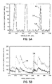
- FIGS. 3A and 3B show optical emission (OE) intensity as a function of wavelength for an oxygen-containing plasma according to an embodiment of the invention.
- a plasma processing system 101 schematically shown in FIG. 2B was utilized to generate plasma from a process gas containing O 2 and Ar.
- FIG. 3A shows an OE feature 300 with maximum intensity at a wavelength of about 844.6 nm that is assigned to light emission from neutral O* radicals in the plasma.
- Curve 310 shows the measured O* intensity for a process gas pressure of 2 Torr
- curve 320 shows the measured O* intensity for a process gas pressure of 50 mTorr.
- the plasma parameters further included an Ar gas flow rate of 2000 standard cubic centimeters per minute (sccm), an O 2 gas flow rate of 200 sccm, and plasma power of 2000 W.
- FIG. 3A shows that increasing the process gas pressure increases the amount of neutral O* radicals in the plasma.
- FIG. 3B shows an OE feature 330 with maximum intensity at a wavelength between about 282 nm and about 283 nm that is assigned to light emission from ionic O 2 + radicals in the plasma.
- Curve 340 shows the measured O 2 + intensity for a process gas pressure of 2 Torr
- curve 350 shows the measured O 2 + intensity for a process gas pressure of 50 mTorr.
- Other plasma parameters were the same as in FIG. 3A .
- FIG. 3B shows that increasing the process gas pressure decreases the amount of ionic O 2 + radicals in the plasma.
- FIGS. 3A and 3B show that the relative amount of neutral O* radicals to ionic O 2 + radicals in an oxygen-containing plasma can be controlled over a wide range by varying the process gas pressure.
- a high process gas pressure allows for generating an oxygen-containing plasma with an increased amount of neutral O* radicals relative to the amount of ionic O 2 + radicals.
- the O*/O 2 + ratio is about 10 at a low pressure of about 50 mTorr and that the O*/O 2 + ratio is about 114 at a high pressure of about 2 Torr.
- FIGS. 4A and 4B show electrical characteristics for a plasma modified gate dielectric stack according to an embodiment of the invention.
- FIG. 4A shows the gate current density of a plasma modified gate dielectric stack as a function of gate voltage.
- Curves 400 and 410 show gate leakage current density (J g ) after modifying a HfSiO x high-k layer ( ⁇ 3 nm thick) with an oxygen-containing plasma generated at high gas pressure (2 Torr), and an oxygen-containing plasma generated at a low gas pressure (50 mTorr), respectively.
- FIG. 4A shows that a HfSiO x high-k layer modified using a high pressure oxygen-containing plasma has near identical gate current density as a HfSiO x high-k layer modified using a low pressure oxygen-containing plasma.
- FIG. 4B shows the capacitance of a plasma modified gate dielectric stack as a function of gate voltage.
- Curves 420 and 430 show the capacitance (C) of a gate dielectric stack after modifying a HfSiO x high-k layer with an oxygen-containing plasma generated at a high process gas pressure, and an oxygen-containing plasma generated at a low process gas pressure, respectively.
- FIG. 4B shows that a HfSiO x high-k layer modified using a high pressure oxygen-containing plasma has a higher capacitance than a HfSiO x layer modified using a low pressure oxygen-containing plasma.
- the equivalent oxide thickness (EOT) of the gate dielectric stack that was modified using a high-pressure oxygen-containing plasma was estimated to be about 1.5 nm, whereas the EOT of the gate dielectric stack that was modified using a high-pressure oxygen-containing plasma was estimated to be about 1.7 nm.
- the results in FIGS. 4A and 4B show that a low pressure oxygen-containing plasma modifies a high-k layer by decreasing the effective dielectric constant of the high-k layer, whereas a high pressure oxygen-containing plasma preserves the thinness of the interfacial oxide layer, thus maintaining the effective dielectric constant of the dielectric stack.
- the high-pressure plasma minimizes the interfacial layer thickness increase during the plasma oxidation, reduces the defects in the layer, incorporates oxygen in the layer, removes carbon impurities from the layer, and yields a lower gate leakage current density than a film exposed to a low-pressure plasma.
- J g in FIG. 4A are comparable to high-k layers that have been annealed at high temperatures.
- embodiments of the current invention provide a method that can minimize high-temperature thermal budgets that can increase the thickness of the interfacial oxide layer.
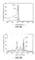
- FIGS. 5A and 5B show OE intensity as a function of wavelength for a nitrogen-containing plasma according to an embodiment of the invention.
- a plasma processing system 101 schematically shown in FIG. 2B was utilized to generate plasma from a process gas containing N 2 and Ar.
- FIG. 5A shows an OE feature 500 with maximum intensity at a wavelength of about 337 nm that is assigned to light emission from neutral N 2 * radicals in the plasma.
- Curve 510 shows the measured N 2 * intensity for a process gas pressure of 200 mTorr
- curve 520 shows the measured N 2 * intensity for a process gas pressure of 800 mTorr, respectively.
- the plasma parameters further included an Ar gas flow rate of about 1000 sccm, a N 2 gas flow rate of about 10 sccm, and plasma power of 2000 W.
- FIG. 5A shows that decreasing the process gas pressure from 800 mTorr to 200 mTorr decreases the amount of neutral N 2 * radicals in the plasma.
- FIG. 5B shows an OE feature 530 with maximum intensity at a wavelength of about 427.2 nm that is assigned to light emission from ionic N 2 + radicals in the plasma.
- Curve 550 shows the measured N 2 + intensity for a gas pressure of 800 mTorr
- curve 540 shows the measured N 2 + intensity for a process gas pressure of 200 mTorr, respectively.
- Other plasma parameters were the same as in FIG. 5A .
- FIG. 5B shows that decreasing the process gas pressure increases the amount of ionic N 2 + radicals in the plasma.
- FIGS. 5A and 5B show that the relative amount of ionic N 2 + radicals to neutral N 2 * radicals in a nitrogen-containing plasma can be controlled over a wide range by varying the process gas pressure.
- a low process gas pressure allows for generating a nitrogen-containing plasma with an increased amount of ionic N 2 + radicals relative to the amount of neutral N 2 * radicals.
- FIG. 6A shows a nitrogen concentration profile in a gate dielectric stack as a function of plasma conditions and as a function of layer depth according to an embodiment of the invention.
- a gate dielectric stack containing a ⁇ 3 nm thick HfSiO x high-k layer deposited onto a substrate was exposed to a nitrogen-containing plasma generated from a process gas containing N 2 and Ar.
- the Si—N fraction indicates the relative amount of a nitrided interface layer.
- the Si—N fraction was measured by time-of-flight secondary ion mass spectroscopy (ToF—SIMS) and sputter depth profiling.
- Curves 610 , 620 , 630 , and 640 show Si—N fraction in plasma modified gate dielectric stacks for different plasma conditions.
- the ratio (R) of ionic nitrogen radicals relative to neutral nitrogen radicals in the plasma decreases from Curve 610 through Curve 640 .
- FIG. 6A shows that a higher amount of ionic nitrogen radicals (i.e., R 610 ) in a plasma resulted in increased nitrogen incorporation into the gate dielectric stack and formation of a thinner nitrided interfacial layer.
- the location (depth) of the maximum nitrogen content was found to decrease with increasing amount of ionic radicals in the plasma, as shown by markers 612 , 622 , and 642 , corresponding to maximum intensities for curves 610 , 620 , and 640 , respectively.
- FIG. 6B shows nitrogen content in a gate dielectric stack as a function of plasma exposure time and as function of layer depth according to an embodiment of the invention.
- the nitrogen content in the gate dielectric stack was found to increase with increasing plasma exposure time.
- FIG. 7 is a flowchart for modifying a gate dielectric stack according to an embodiment of the invention.
- the method uses a plasma process to modify the gate dielectric stack and improve the properties of the high-k layer while minimizing the growth of an interfacial layer on the substrate.
- the process 700 is started at 710 .
- a gate dielectric stack containing a high-k layer on a substrate is provided.
- the substrate can contain an interfacial layer located between the substrate and the high-k layer.
- plasma is generated from a process gas containing an inert gas and an oxygen-containing gas, or an inert gas and a nitrogen-containing gas, wherein the process gas pressure is selected to control the amount of neutral radicals relative to the amount of ionic radicals in the plasma.
- a plasma is generated at 730 from a process gas containing an inert gas and an oxygen-containing gas, where a high process gas pressure is selected to increase the amount of neutral oxygen radicals relative to the amount of ionic oxygen radicals in the plasma.
- the high-pressure oxygen-containing plasma is capable of modifying the gate dielectric stack by increasing the dielectric constant of the high-k layer through reducing defects in the layer, incorporating oxygen in the layer, and removing carbon impurities from the layer.
- plasma is generated at 730 from a process gas containing an inert gas and a nitrogen-containing gas, where a low process gas pressure is selected to increase the amount of ionic nitrogen radicals relative to the amount of neutral nitrogen radicals in the plasma.
- the low-pressure nitrogen-containing plasma is capable of increasing the nitrogen content of the gate dielectric stack and form a thin nitrided interfacial layer.
- the stack is modified by exposing the stack to the high-pressure oxygen-containing plasma or the low-pressure nitrogen-containing plasma.
- the process is ended at 750 .
- the stack is exposed to the oxygen-containing plasma for a time period between about 5 seconds and about 60 seconds.
- the stack is exposed to the nitrogen-containing plasma for a time period between about 60 seconds and about 300 seconds.
- the substrate may be maintained at a temperature between about 150° C. and about 450° C. during the modification.
- a gate dielectric stack can be modified by exposure to a high-pressure oxygen-containing plasma, wherein the plasma contains increased amount of neutral oxygen radicals relative to the amount of ionic oxygen radicals in the plasma and, subsequently, the resulting stack can be further modified by exposure to a low-pressure nitrogen-containing plasma, wherein the plasma contains an increased amount of ionic nitrogen radicals relative to the amount of neutral nitrogen radicals in the plasma.
- 730 and 740 are performed a first time using the high-pressure oxygen-containing plasma, and then 730 and 740 are performed a second time, as indicated by the dashed line in FIG. 7 , using the low-pressure nitrogen-containing plasma, and then the process is ended at 750 .
- a gate dielectric stack can be modified by exposure to a low-pressure nitrogen-containing plasma, wherein the plasma contains an increased amount of ionic nitrogen radicals relative to the amount of neutral nitrogen radicals in the plasma and, subsequently, the resulting stack can be further modified by exposure to a high-pressure oxygen-containing plasma, wherein the plasma contains increased amount of neutral oxygen radicals relative to the amount of ionic oxygen radicals in the plasma.
- 730 and 740 are performed a first time using the low-pressure nitrogen-containing plasma, and then 730 and 740 are performed a second time, as indicated by the dashed line in FIG. 7 , using the high-pressure oxygen-containing plasma, and then the process is ended at 750 .
- the high-pressure oxygen-containing plasma process and the low-pressure nitrogen-containing plasma processes described above can be performed sequentially in the same plasma processing system within a cluster tool or, alternatively, they can be performed in different plasma processing systems within the same cluster tool.
- the cluster tool can further contain a substrate transfer system configured for transferring substrates within the cluster tool, and a controller configured to control the components of the cluster tool.
Abstract
Description
Claims (51)
Priority Applications (6)
| Application Number | Priority Date | Filing Date | Title |
|---|---|---|---|
| US10/920,990 US7163877B2 (en) | 2004-08-18 | 2004-08-18 | Method and system for modifying a gate dielectric stack containing a high-k layer using plasma processing |
| CNB2005800274871A CN100568462C (en) | 2004-08-18 | 2005-08-11 | Improve the method and system of the gate dielectric stack that comprises high-k layer with plasma treatment |
| KR1020077003092A KR101163264B1 (en) | 2004-08-18 | 2005-08-11 | A method for modifying a gate dielectric stack containing a high-k layer using plasma processing |
| PCT/US2005/028610 WO2006023373A1 (en) | 2004-08-18 | 2005-08-11 | A method and system for modifying a gate dielectric stack containing a high-k layer using plasma processing |
| JP2007527883A JP4950888B2 (en) | 2004-08-18 | 2005-08-11 | Method for improving gate dielectric stacks with high dielectric constant layers using plasma treatment |
| TW094128198A TWI268553B (en) | 2004-08-18 | 2005-08-18 | A method and system for modifying a gate dielectric stack containing a high-k layer using plasma processing |
Applications Claiming Priority (1)
| Application Number | Priority Date | Filing Date | Title |
|---|---|---|---|
| US10/920,990 US7163877B2 (en) | 2004-08-18 | 2004-08-18 | Method and system for modifying a gate dielectric stack containing a high-k layer using plasma processing |
Publications (2)
| Publication Number | Publication Date |
|---|---|
| US20060040483A1 US20060040483A1 (en) | 2006-02-23 |
| US7163877B2 true US7163877B2 (en) | 2007-01-16 |
Family
ID=35431477
Family Applications (1)
| Application Number | Title | Priority Date | Filing Date |
|---|---|---|---|
| US10/920,990 Active 2025-02-14 US7163877B2 (en) | 2004-08-18 | 2004-08-18 | Method and system for modifying a gate dielectric stack containing a high-k layer using plasma processing |
Country Status (6)
| Country | Link |
|---|---|
| US (1) | US7163877B2 (en) |
| JP (1) | JP4950888B2 (en) |
| KR (1) | KR101163264B1 (en) |
| CN (1) | CN100568462C (en) |
| TW (1) | TWI268553B (en) |
| WO (1) | WO2006023373A1 (en) |
Cited By (14)
| Publication number | Priority date | Publication date | Assignee | Title |
|---|---|---|---|---|
| US20070049048A1 (en) * | 2005-08-31 | 2007-03-01 | Shahid Rauf | Method and apparatus for improving nitrogen profile during plasma nitridation |
| US20070287925A1 (en) * | 2006-05-13 | 2007-12-13 | Katayama Andrew S | Continuous positioning apparatus and methods |
| US20090233430A1 (en) * | 2008-02-19 | 2009-09-17 | Hitachi-Kokusai Electric In. | Semiconductor device manufacturing method, semiconductor device manufacturing apparatus, and semiconductor device manufacturing system |
| US20100044803A1 (en) * | 2008-08-25 | 2010-02-25 | Taiwan Semiconductor Manufacturing Company, Ltd. | Sealing structure for high-k metal gate and method of making |
| US20100044804A1 (en) * | 2008-08-25 | 2010-02-25 | Taiwan Semiconductor Manufacturing Company, Ltd. | Novel high-k metal gate structure and method of making |
| US20100099247A1 (en) * | 2008-10-21 | 2010-04-22 | Applied Materials Inc. | Flash memory with treated charge trap layer |
| US20100270609A1 (en) * | 2009-04-22 | 2010-10-28 | Applied Materials, Inc. | Modification of charge trap silicon nitride with oxygen plasma |
| US20110124202A1 (en) * | 2004-03-03 | 2011-05-26 | Tokyo Electron Limited | Plasma processing method and computer storage medium |
| CN103843465A (en) * | 2011-10-13 | 2014-06-04 | 韩国科学技术院 | Plasma apparatus and substrate-processing apparatus |
| US20140342575A1 (en) * | 2013-05-15 | 2014-11-20 | Tokyo Electron Limited | Method for Forming an Interfacial Layer on a Semiconductor Using Hydrogen Plasma |
| US9655530B2 (en) | 2011-04-29 | 2017-05-23 | Tensys Medical, Inc. | Apparatus and methods for non-invasively measuring physiologic parameters of one or more subjects |
| US9960011B2 (en) | 2011-08-01 | 2018-05-01 | Plasmart Inc. | Plasma generation apparatus and plasma generation method |
| US10797160B2 (en) | 2018-01-31 | 2020-10-06 | Samsung Electronics Co., Ltd. | Methods of fabricating semiconductor devices |
| US10952675B2 (en) | 2007-10-12 | 2021-03-23 | Shangyi Medical Technology (Hangzhou) Co., Ltd | Apparatus and methods for non-invasively measuring a patient's arterial blood pressure |
Families Citing this family (15)
| Publication number | Priority date | Publication date | Assignee | Title |
|---|---|---|---|---|
| WO2007132884A1 (en) * | 2006-05-17 | 2007-11-22 | Hitachi Kokusai Electric Inc. | Semiconductor device manufacturing method and substrate processing apparatus |
| US7964515B2 (en) * | 2007-12-21 | 2011-06-21 | Tokyo Electron Limited | Method of forming high-dielectric constant films for semiconductor devices |
| US8962454B2 (en) * | 2010-11-04 | 2015-02-24 | Tokyo Electron Limited | Method of depositing dielectric films using microwave plasma |
| KR101893471B1 (en) * | 2011-02-15 | 2018-08-30 | 어플라이드 머티어리얼스, 인코포레이티드 | Method and apparatus for multizone plasma generation |
| US8890264B2 (en) * | 2012-09-26 | 2014-11-18 | Intel Corporation | Non-planar III-V field effect transistors with conformal metal gate electrode and nitrogen doping of gate dielectric interface |
| US9224644B2 (en) * | 2012-12-26 | 2015-12-29 | Intermolecular, Inc. | Method to control depth profiles of dopants using a remote plasma source |
| US9331168B2 (en) | 2014-01-17 | 2016-05-03 | Taiwan Semiconductor Manufacturing Company Ltd. | Semiconductor structure and manufacuturing method of the same |
| CN104821276B (en) * | 2014-01-30 | 2018-08-10 | 中芯国际集成电路制造(上海)有限公司 | The production method of MOS transistor |
| JP2018528619A (en) * | 2015-09-18 | 2018-09-27 | 東京エレクトロン株式会社 | Germanium-containing semiconductor device and formation method |
| JP6671166B2 (en) * | 2015-12-15 | 2020-03-25 | 東京エレクトロン株式会社 | Method for manufacturing insulating film laminate |
| US11152214B2 (en) * | 2016-04-20 | 2021-10-19 | International Business Machines Corporation | Structures and methods for equivalent oxide thickness scaling on silicon germanium channel or III-V channel of semiconductor device |
| TWI635539B (en) * | 2017-09-15 | 2018-09-11 | 金巨達國際股份有限公司 | High-k dielectric layer, fabricating method thereof and multifunction equipment implementing such fabricating method |
| CN108735607A (en) * | 2018-05-25 | 2018-11-02 | 中国科学院微电子研究所 | The manufacturing method of groove MOSFET element based on microwave plasma oxidation |
| US20210057215A1 (en) * | 2019-05-03 | 2021-02-25 | Applied Materials, Inc. | Treatments to enhance material structures |
| US20210193468A1 (en) * | 2019-05-03 | 2021-06-24 | Applied Materials, Inc. | Treatments To Improve Device Performance |
Citations (9)
| Publication number | Priority date | Publication date | Assignee | Title |
|---|---|---|---|---|
| US20030025146A1 (en) | 2001-07-23 | 2003-02-06 | Pravin Narwankar | Processes for making a barrier between a dielectric and a conductor and products produced therefrom |
| WO2004004014A1 (en) | 2002-06-27 | 2004-01-08 | Nec Corporation | Semiconductor device and its manufacturing method |
| US20040009642A1 (en) | 2002-07-10 | 2004-01-15 | Samsung Electronics Co., Ltd. | Method of fabricating non-volatile memory device having a structure of silicon-oxide-nitride-oxide-silicon |
| US6709715B1 (en) * | 1999-06-17 | 2004-03-23 | Applied Materials Inc. | Plasma enhanced chemical vapor deposition of copolymer of parylene N and comonomers with various double bonds |
| US6730566B2 (en) | 2002-10-04 | 2004-05-04 | Texas Instruments Incorporated | Method for non-thermally nitrided gate formation for high voltage devices |
| WO2004044898A2 (en) | 2002-11-08 | 2004-05-27 | Aviza Technology, Inc. | Nitridation of high-k dielectrics |
| US20040110361A1 (en) | 2002-12-10 | 2004-06-10 | Parker Christopher G. | Method for making a semiconductor device having an ultra-thin high-k gate dielectric |
| US6787861B2 (en) * | 2000-06-26 | 2004-09-07 | North Carolina State University | Non-crystalline oxides for use in microelectronic, optical, and other applications |
| US20050106893A1 (en) * | 2003-08-04 | 2005-05-19 | Glen Wilk | Surface preparation prior to deposition on germanium |
Family Cites Families (6)
| Publication number | Priority date | Publication date | Assignee | Title |
|---|---|---|---|---|
| JPH05221644A (en) * | 1992-02-13 | 1993-08-31 | Matsushita Electric Ind Co Ltd | Production of thin tantalum oxide film |
| JP3230901B2 (en) * | 1993-06-22 | 2001-11-19 | 株式会社東芝 | Semiconductor device manufacturing method and manufacturing apparatus |
| JPH0964307A (en) * | 1995-08-29 | 1997-03-07 | Hitachi Ltd | Heat treatment method of oxide thin film |
| EP1265279B1 (en) * | 2000-03-13 | 2009-10-14 | OHMI, Tadahiro | Method of fabricating a flash memory device |
| JP2004228355A (en) * | 2003-01-23 | 2004-08-12 | Seiko Epson Corp | Insulating film substrate, method and apparatus for manufacturing the same, electro-optical device and method for manufacturing the same |
| JP4280686B2 (en) * | 2004-06-30 | 2009-06-17 | キヤノン株式会社 | Processing method |
-
2004
- 2004-08-18 US US10/920,990 patent/US7163877B2/en active Active
-
2005
- 2005-08-11 WO PCT/US2005/028610 patent/WO2006023373A1/en active Application Filing
- 2005-08-11 KR KR1020077003092A patent/KR101163264B1/en active IP Right Grant
- 2005-08-11 CN CNB2005800274871A patent/CN100568462C/en not_active Expired - Fee Related
- 2005-08-11 JP JP2007527883A patent/JP4950888B2/en not_active Expired - Fee Related
- 2005-08-18 TW TW094128198A patent/TWI268553B/en not_active IP Right Cessation
Patent Citations (10)
| Publication number | Priority date | Publication date | Assignee | Title |
|---|---|---|---|---|
| US6709715B1 (en) * | 1999-06-17 | 2004-03-23 | Applied Materials Inc. | Plasma enhanced chemical vapor deposition of copolymer of parylene N and comonomers with various double bonds |
| US6787861B2 (en) * | 2000-06-26 | 2004-09-07 | North Carolina State University | Non-crystalline oxides for use in microelectronic, optical, and other applications |
| US20030025146A1 (en) | 2001-07-23 | 2003-02-06 | Pravin Narwankar | Processes for making a barrier between a dielectric and a conductor and products produced therefrom |
| WO2004004014A1 (en) | 2002-06-27 | 2004-01-08 | Nec Corporation | Semiconductor device and its manufacturing method |
| US20050247985A1 (en) | 2002-06-27 | 2005-11-10 | Heiji Watanabe | Semiconductor device and its manufacturing method |
| US20040009642A1 (en) | 2002-07-10 | 2004-01-15 | Samsung Electronics Co., Ltd. | Method of fabricating non-volatile memory device having a structure of silicon-oxide-nitride-oxide-silicon |
| US6730566B2 (en) | 2002-10-04 | 2004-05-04 | Texas Instruments Incorporated | Method for non-thermally nitrided gate formation for high voltage devices |
| WO2004044898A2 (en) | 2002-11-08 | 2004-05-27 | Aviza Technology, Inc. | Nitridation of high-k dielectrics |
| US20040110361A1 (en) | 2002-12-10 | 2004-06-10 | Parker Christopher G. | Method for making a semiconductor device having an ultra-thin high-k gate dielectric |
| US20050106893A1 (en) * | 2003-08-04 | 2005-05-19 | Glen Wilk | Surface preparation prior to deposition on germanium |
Non-Patent Citations (4)
| Title |
|---|
| Chris Hinkle et al., Remote Plasma-Assisted Nitridation (RPN): Applications to Zr and Hf Silicate Alloys and Al<SUB>2</SUB>O<SUB>3</SUB>, Applied Surface Science 216 (2003) pp. 124-132. |
| European Patent Office. International Search Report and Written Opinion, PCT/US2005/028610, dated Dec. 29, 2005, 11 pp. |
| Gerald Lucovsky et al., Plasma Processed Ultra-thin SiO2, Interfaces for Advanced Silicon NMOS and PMOS Devices; Applications to Si-Oxide/Si Oxynitride, Si-Oxide/Sl Nitride and Si-Oxide/Transition Metal Oxide Slacked Gate Dielectrics, Thin Solid Films 374 (2000) pp. 217-227. |
| Seiji Inumiya et al., Fabrication of HfSiON Gate Dielectrics by Plasma Oxidation and Nitridation, Optimized for 66nm Node Low Power CMOS Applications, 2003 Symposium on VLSI Technology Digest of Technical Papers, pp. 17-18. |
Cited By (26)
| Publication number | Priority date | Publication date | Assignee | Title |
|---|---|---|---|---|
| US20110124202A1 (en) * | 2004-03-03 | 2011-05-26 | Tokyo Electron Limited | Plasma processing method and computer storage medium |
| US8183165B2 (en) * | 2004-03-03 | 2012-05-22 | Tokyo Electron Limited | Plasma processing method |
| US20070049048A1 (en) * | 2005-08-31 | 2007-03-01 | Shahid Rauf | Method and apparatus for improving nitrogen profile during plasma nitridation |
| US10285598B2 (en) | 2006-05-13 | 2019-05-14 | United States Gtm Medical Devices | Continuous positioning apparatus and methods |
| US20070287925A1 (en) * | 2006-05-13 | 2007-12-13 | Katayama Andrew S | Continuous positioning apparatus and methods |
| US9107588B2 (en) | 2006-05-13 | 2015-08-18 | Tensys Medical, Inc. | Continuous positioning apparatus and methods |
| US8506497B2 (en) | 2006-05-13 | 2013-08-13 | Tensys Medical, Inc. | Continuous positioning apparatus and methods |
| US10952675B2 (en) | 2007-10-12 | 2021-03-23 | Shangyi Medical Technology (Hangzhou) Co., Ltd | Apparatus and methods for non-invasively measuring a patient's arterial blood pressure |
| US20090233430A1 (en) * | 2008-02-19 | 2009-09-17 | Hitachi-Kokusai Electric In. | Semiconductor device manufacturing method, semiconductor device manufacturing apparatus, and semiconductor device manufacturing system |
| US20100044803A1 (en) * | 2008-08-25 | 2010-02-25 | Taiwan Semiconductor Manufacturing Company, Ltd. | Sealing structure for high-k metal gate and method of making |
| US20100044804A1 (en) * | 2008-08-25 | 2010-02-25 | Taiwan Semiconductor Manufacturing Company, Ltd. | Novel high-k metal gate structure and method of making |
| US8450161B2 (en) | 2008-08-25 | 2013-05-28 | Taiwan Semiconductor Manufacturing Company, Ltd. | Method of fabricating a sealing structure for high-k metal gate |
| US8193586B2 (en) | 2008-08-25 | 2012-06-05 | Taiwan Semiconductor Manufacturing Company, Ltd. | Sealing structure for high-K metal gate |
| US7816205B2 (en) | 2008-10-21 | 2010-10-19 | Applied Materials, Inc. | Method of forming non-volatile memory having charge trap layer with compositional gradient |
| US8501568B2 (en) | 2008-10-21 | 2013-08-06 | Applied Materials, Inc. | Method of forming flash memory with ultraviolet treatment |
| US8252653B2 (en) | 2008-10-21 | 2012-08-28 | Applied Materials, Inc. | Method of forming a non-volatile memory having a silicon nitride charge trap layer |
| US20100099247A1 (en) * | 2008-10-21 | 2010-04-22 | Applied Materials Inc. | Flash memory with treated charge trap layer |
| US8198671B2 (en) | 2009-04-22 | 2012-06-12 | Applied Materials, Inc. | Modification of charge trap silicon nitride with oxygen plasma |
| US20100270609A1 (en) * | 2009-04-22 | 2010-10-28 | Applied Materials, Inc. | Modification of charge trap silicon nitride with oxygen plasma |
| US9655530B2 (en) | 2011-04-29 | 2017-05-23 | Tensys Medical, Inc. | Apparatus and methods for non-invasively measuring physiologic parameters of one or more subjects |
| US9960011B2 (en) | 2011-08-01 | 2018-05-01 | Plasmart Inc. | Plasma generation apparatus and plasma generation method |
| CN103843465A (en) * | 2011-10-13 | 2014-06-04 | 韩国科学技术院 | Plasma apparatus and substrate-processing apparatus |
| US9734990B2 (en) | 2011-10-13 | 2017-08-15 | Korea Advanced Institute Of Science And Technology | Plasma apparatus and substrate-processing apparatus |
| US20140342575A1 (en) * | 2013-05-15 | 2014-11-20 | Tokyo Electron Limited | Method for Forming an Interfacial Layer on a Semiconductor Using Hydrogen Plasma |
| US9343291B2 (en) * | 2013-05-15 | 2016-05-17 | Tokyo Electron Limited | Method for forming an interfacial layer on a semiconductor using hydrogen plasma |
| US10797160B2 (en) | 2018-01-31 | 2020-10-06 | Samsung Electronics Co., Ltd. | Methods of fabricating semiconductor devices |
Also Published As
| Publication number | Publication date |
|---|---|
| KR101163264B1 (en) | 2012-07-05 |
| CN100568462C (en) | 2009-12-09 |
| CN101006566A (en) | 2007-07-25 |
| WO2006023373A1 (en) | 2006-03-02 |
| JP4950888B2 (en) | 2012-06-13 |
| KR20080009675A (en) | 2008-01-29 |
| TW200618091A (en) | 2006-06-01 |
| JP2008510319A (en) | 2008-04-03 |
| TWI268553B (en) | 2006-12-11 |
| US20060040483A1 (en) | 2006-02-23 |
Similar Documents
| Publication | Publication Date | Title |
|---|---|---|
| US7163877B2 (en) | Method and system for modifying a gate dielectric stack containing a high-k layer using plasma processing | |
| JP5042038B2 (en) | Method for manufacturing a semiconductor device | |
| US8021987B2 (en) | Method of modifying insulating film | |
| US7902018B2 (en) | Fluorine plasma treatment of high-k gate stack for defect passivation | |
| US7678710B2 (en) | Method and apparatus for fabricating a high dielectric constant transistor gate using a low energy plasma system | |
| US20230178419A1 (en) | Scaled liner layer for isolation structure | |
| US8158535B2 (en) | Method for forming insulating film and method for manufacturing semiconductor device | |
| US8043981B2 (en) | Dual frequency low temperature oxidation of a semiconductor device | |
| KR101117450B1 (en) | Method and apparatus for fabricating a high dielectric constant transistor gate using a low energy plasma system | |
| US20070209930A1 (en) | Apparatus for fabricating a high dielectric constant transistor gate using a low energy plasma system | |
| US20060269694A1 (en) | Plasma processing method | |
| TWI423333B (en) | Method and apparatus for fabricating a high dielectric constant transistor gate using a low energy plasma system | |
| US8501628B2 (en) | Differential metal gate etching process | |
| US7517812B2 (en) | Method and system for forming a nitrided germanium-containing layer using plasma processing | |
| US7517818B2 (en) | Method for forming a nitrided germanium-containing layer using plasma processing | |
| TWI459471B (en) | Method and apparatus for fabricating a high dielectric constant transistor gate using a low energy plasma system | |
| US6780788B2 (en) | Methods for improving within-wafer uniformity of gate oxide | |
| US20030194510A1 (en) | Methods used in fabricating gates in integrated circuit device structures | |
| TWI442474B (en) | Methods for forming conformal oxide layers on semiconductor devices |
Legal Events
| Date | Code | Title | Description |
|---|---|---|---|
| AS | Assignment |
Owner name: TOKYO ELECTRON LIMITED, JAPAN Free format text: ASSIGNMENT OF ASSIGNORS INTEREST;ASSIGNORS:NIIMI, HIROAKI;COLOMBO, LUIGI;SHIMOMURA, KOJI;AND OTHERS;REEL/FRAME:015390/0673;SIGNING DATES FROM 20041023 TO 20041104 Owner name: TEXAS INSTRUMENTS INCORPORATED, TEXAS Free format text: ASSIGNMENT OF ASSIGNORS INTEREST;ASSIGNORS:NIIMI, HIROAKI;COLOMBO, LUIGI;SHIMOMURA, KOJI;AND OTHERS;REEL/FRAME:015390/0673;SIGNING DATES FROM 20041023 TO 20041104 |
|
| AS | Assignment |
Owner name: TOKYO ELECTRON LIMITED, JAPAN Free format text: CORRECTIVE DOCUMENT;ASSIGNORS:NIIMI, HIROAKI;COLOMBO, LUIGI;SHIMOMURA, KOJI;AND OTHERS;REEL/FRAME:016305/0877;SIGNING DATES FROM 20041026 TO 20041104 Owner name: TEXAS INSTRUMENTS INCORPORATED, TEXAS Free format text: CORRECTIVE DOCUMENT;ASSIGNORS:NIIMI, HIROAKI;COLOMBO, LUIGI;SHIMOMURA, KOJI;AND OTHERS;REEL/FRAME:016305/0877;SIGNING DATES FROM 20041026 TO 20041104 |
|
| AS | Assignment |
Owner name: TOKYO ELECTRON LIMITED, JAPAN Free format text: TO CORRECT EXECUTION DATE ON REEL 015390 FRAME 0673.;ASSIGNORS:NIIMI, HIROAKI;COLOMBO, LUIGI;SHIMOMURA, KOJI;AND OTHERS;REEL/FRAME:016509/0889;SIGNING DATES FROM 20041026 TO 20041104 Owner name: TEXAS INSTRUMENTS INCORPORATED, TEXAS Free format text: TO CORRECT EXECUTION DATE ON REEL 015390 FRAME 0673.;ASSIGNORS:NIIMI, HIROAKI;COLOMBO, LUIGI;SHIMOMURA, KOJI;AND OTHERS;REEL/FRAME:016509/0889;SIGNING DATES FROM 20041026 TO 20041104 |
|
| STCF | Information on status: patent grant |
Free format text: PATENTED CASE |
|
| CC | Certificate of correction | ||
| FEPP | Fee payment procedure |
Free format text: PAYOR NUMBER ASSIGNED (ORIGINAL EVENT CODE: ASPN); ENTITY STATUS OF PATENT OWNER: LARGE ENTITY |
|
| FPAY | Fee payment |
Year of fee payment: 4 |
|
| FPAY | Fee payment |
Year of fee payment: 8 |
|
| MAFP | Maintenance fee payment |
Free format text: PAYMENT OF MAINTENANCE FEE, 12TH YEAR, LARGE ENTITY (ORIGINAL EVENT CODE: M1553) Year of fee payment: 12 |