US7130002B2 - LCD with metal diffused into the insulating layer over the channel area - Google Patents
LCD with metal diffused into the insulating layer over the channel area Download PDFInfo
- Publication number
- US7130002B2 US7130002B2 US10/875,564 US87556404A US7130002B2 US 7130002 B2 US7130002 B2 US 7130002B2 US 87556404 A US87556404 A US 87556404A US 7130002 B2 US7130002 B2 US 7130002B2
- Authority
- US
- United States
- Prior art keywords
- silicon film
- liquid crystal
- source
- display panel
- crystal display
- Prior art date
- Legal status (The legal status is an assumption and is not a legal conclusion. Google has not performed a legal analysis and makes no representation as to the accuracy of the status listed.)
- Active, expires
Links
Images


Classifications
-
- G—PHYSICS
- G02—OPTICS
- G02F—OPTICAL DEVICES OR ARRANGEMENTS FOR THE CONTROL OF LIGHT BY MODIFICATION OF THE OPTICAL PROPERTIES OF THE MEDIA OF THE ELEMENTS INVOLVED THEREIN; NON-LINEAR OPTICS; FREQUENCY-CHANGING OF LIGHT; OPTICAL LOGIC ELEMENTS; OPTICAL ANALOGUE/DIGITAL CONVERTERS
- G02F1/00—Devices or arrangements for the control of the intensity, colour, phase, polarisation or direction of light arriving from an independent light source, e.g. switching, gating or modulating; Non-linear optics
- G02F1/01—Devices or arrangements for the control of the intensity, colour, phase, polarisation or direction of light arriving from an independent light source, e.g. switching, gating or modulating; Non-linear optics for the control of the intensity, phase, polarisation or colour
- G02F1/13—Devices or arrangements for the control of the intensity, colour, phase, polarisation or direction of light arriving from an independent light source, e.g. switching, gating or modulating; Non-linear optics for the control of the intensity, phase, polarisation or colour based on liquid crystals, e.g. single liquid crystal display cells
- G02F1/133—Constructional arrangements; Operation of liquid crystal cells; Circuit arrangements
- G02F1/136—Liquid crystal cells structurally associated with a semi-conducting layer or substrate, e.g. cells forming part of an integrated circuit
- G02F1/1362—Active matrix addressed cells
- G02F1/1368—Active matrix addressed cells in which the switching element is a three-electrode device
-
- H—ELECTRICITY
- H01—ELECTRIC ELEMENTS
- H01L—SEMICONDUCTOR DEVICES NOT COVERED BY CLASS H10
- H01L27/00—Devices consisting of a plurality of semiconductor or other solid-state components formed in or on a common substrate
- H01L27/02—Devices consisting of a plurality of semiconductor or other solid-state components formed in or on a common substrate including semiconductor components specially adapted for rectifying, oscillating, amplifying or switching and having at least one potential-jump barrier or surface barrier; including integrated passive circuit elements with at least one potential-jump barrier or surface barrier
- H01L27/12—Devices consisting of a plurality of semiconductor or other solid-state components formed in or on a common substrate including semiconductor components specially adapted for rectifying, oscillating, amplifying or switching and having at least one potential-jump barrier or surface barrier; including integrated passive circuit elements with at least one potential-jump barrier or surface barrier the substrate being other than a semiconductor body, e.g. an insulating body
- H01L27/1214—Devices consisting of a plurality of semiconductor or other solid-state components formed in or on a common substrate including semiconductor components specially adapted for rectifying, oscillating, amplifying or switching and having at least one potential-jump barrier or surface barrier; including integrated passive circuit elements with at least one potential-jump barrier or surface barrier the substrate being other than a semiconductor body, e.g. an insulating body comprising a plurality of TFTs formed on a non-semiconducting substrate, e.g. driving circuits for AMLCDs
- H01L27/1259—Multistep manufacturing methods
- H01L27/127—Multistep manufacturing methods with a particular formation, treatment or patterning of the active layer specially adapted to the circuit arrangement
- H01L27/1274—Multistep manufacturing methods with a particular formation, treatment or patterning of the active layer specially adapted to the circuit arrangement using crystallisation of amorphous semiconductor or recrystallisation of crystalline semiconductor
- H01L27/1277—Multistep manufacturing methods with a particular formation, treatment or patterning of the active layer specially adapted to the circuit arrangement using crystallisation of amorphous semiconductor or recrystallisation of crystalline semiconductor using a crystallisation promoting species, e.g. local introduction of Ni catalyst
-
- H—ELECTRICITY
- H01—ELECTRIC ELEMENTS
- H01L—SEMICONDUCTOR DEVICES NOT COVERED BY CLASS H10
- H01L27/00—Devices consisting of a plurality of semiconductor or other solid-state components formed in or on a common substrate
- H01L27/02—Devices consisting of a plurality of semiconductor or other solid-state components formed in or on a common substrate including semiconductor components specially adapted for rectifying, oscillating, amplifying or switching and having at least one potential-jump barrier or surface barrier; including integrated passive circuit elements with at least one potential-jump barrier or surface barrier
- H01L27/12—Devices consisting of a plurality of semiconductor or other solid-state components formed in or on a common substrate including semiconductor components specially adapted for rectifying, oscillating, amplifying or switching and having at least one potential-jump barrier or surface barrier; including integrated passive circuit elements with at least one potential-jump barrier or surface barrier the substrate being other than a semiconductor body, e.g. an insulating body
- H01L27/1214—Devices consisting of a plurality of semiconductor or other solid-state components formed in or on a common substrate including semiconductor components specially adapted for rectifying, oscillating, amplifying or switching and having at least one potential-jump barrier or surface barrier; including integrated passive circuit elements with at least one potential-jump barrier or surface barrier the substrate being other than a semiconductor body, e.g. an insulating body comprising a plurality of TFTs formed on a non-semiconducting substrate, e.g. driving circuits for AMLCDs
- H01L27/1259—Multistep manufacturing methods
- H01L27/1288—Multistep manufacturing methods employing particular masking sequences or specially adapted masks, e.g. half-tone mask
-
- H—ELECTRICITY
- H01—ELECTRIC ELEMENTS
- H01L—SEMICONDUCTOR DEVICES NOT COVERED BY CLASS H10
- H01L21/00—Processes or apparatus adapted for the manufacture or treatment of semiconductor or solid state devices or of parts thereof
- H01L21/02—Manufacture or treatment of semiconductor devices or of parts thereof
- H01L21/02104—Forming layers
- H01L21/02365—Forming inorganic semiconducting materials on a substrate
- H01L21/02518—Deposited layers
- H01L21/02521—Materials
- H01L21/02524—Group 14 semiconducting materials
- H01L21/02532—Silicon, silicon germanium, germanium
-
- H—ELECTRICITY
- H01—ELECTRIC ELEMENTS
- H01L—SEMICONDUCTOR DEVICES NOT COVERED BY CLASS H10
- H01L21/00—Processes or apparatus adapted for the manufacture or treatment of semiconductor or solid state devices or of parts thereof
- H01L21/02—Manufacture or treatment of semiconductor devices or of parts thereof
- H01L21/02104—Forming layers
- H01L21/02365—Forming inorganic semiconducting materials on a substrate
- H01L21/02656—Special treatments
- H01L21/02664—Aftertreatments
- H01L21/02667—Crystallisation or recrystallisation of non-monocrystalline semiconductor materials, e.g. regrowth
- H01L21/02672—Crystallisation or recrystallisation of non-monocrystalline semiconductor materials, e.g. regrowth using crystallisation enhancing elements
Definitions
- the present invention relates to a liquid crystal display panel using polycrystalline silicon, and more particularly, to a liquid crystal display panel and a method of fabricating thereof that is capable of enhancing the crystallization efficiency of an active layer and reducing the number of fabricating processes.
- liquid crystal displays control the light transmittance of liquid crystal cells in accordance with video signals, thereby displaying pictures corresponding to the video signals on a liquid crystal display panel where the liquid crystal cells are arranged in a matrix form.
- a thin film transistor TFT is typically used as a switching device for the liquid crystal cells.
- the semiconductor layer of such a thin film transistor is made of either amorphous silicon or polycrystalline silicon.
- Amorphous silicon TFTs have an advantage in that they have relatively better uniformity and stable property.
- the amorphous silicon TFTs also have a disadvantage in that response speed is slow because the carrier mobility of amorphous silicon is low.
- polycrystalline silicon TFTs have drawn attention for the applications of liquid crystal display panels with a high resolution and peripheral driving circuits mounted in the display panels.
- FIG. 1 and FIG. 2 are a plan view and a sectional view of a related art liquid crystal display panel having such a polycrystalline silicon TFT.
- the liquid crystal display panel having the thin film transistor includes a gate line 2 , a data line 4 crossing the gate line 2 with an insulating film 12 therebetween, a TFT 30 provided at a crossing of the gate line 2 and the data line 4 , and a pixel electrode 22 provided in a pixel area defined by the crossing of the gate line 2 and the data line 4 .
- the gate line 2 applies a gate signal to a gate electrode 6 of the TFT 30 .
- the data line 4 applies a pixel signal to the pixel electrode 22 via a drain electrode 10 of the TFT 30 .
- the TFT 30 includes the gate electrode 6 connected to the gate line 2 , a source electrode 8 connected to the data line 4 and a drain electrode 10 connected, via a contact hole 20 passing through a passivation film 18 , to the pixel electrode 22 .
- the gate electrode 6 is formed on a buffer film 16 so as to overlap a channel area 14 C of the active layer, with the gate insulating film 12 between the gate electrode 6 and the channel area 14 C.
- the source electrode 8 is formed to be insulated from the gate electrode 6 with the gate insulating film 12 therebetween and to be directly connected to a source area 14 S of the active layer.
- the drain electrode 10 is formed to be insulated from the gate electrode 6 with the gate insulating film 12 therebetween and to be connected to a drain area 14 D of the active layer. Different ions, depending on the location of the active layer 14 and type of the TFT 30 , are injected into the active layer 14 .
- the TFT 30 has an N channel, at least one of n + and n ⁇ ions is injected into the active layer.
- the active layer to which the n ⁇ ions are injected becomes a Lightly Doped Drain (LDD) area, which is generally used to reduce the off-current of the TFT 30 .
- LDD Lightly Doped Drain
- the active layer into which the n + ions are injected becomes the source area and the drain area, and the active layer into which the n + and n ⁇ ions are not injected become the channel area.
- the TFT 30 has a P channel, p + ions are injected into the active layer. While the active layer into which the p + ions are injected becomes the source and the drain areas, the active layer into which the p + ions are not injected become the channel area.
- Such a TFT 30 responds to a scanning pulse applied from the gate line 2 , to thereby allow a video signal, that is, a pixel signal applied from the data line 4 , to be charged in a liquid crystal cell.
- a video signal that is, a pixel signal applied from the data line 4
- the liquid crystal cell controls a light transmittance in accordance with the pixel signal.
- FIGS. 3A to 3F are sectional views illustrating a fabricating process of a liquid crystal display having polycrystalline silicon TFTs.
- an insulating material such as silicon oxide SiO 2 is deposited on the entire lower substrate 1 , thereby forming a buffer film 16 , as shown in FIG. 3A .
- a gate metal layer is deposited on the entire surface of the lower substrate 1 with the buffer film 16 thereon, and then the gate metal layer is patterned by photolithography and etching processes including exposing and developing steps, thereby forming a gate electrode 6 .
- the gate metal layer may be made of a metal including aluminum and aluminum/neodymium, etc.
- a gate insulating material such as silicon oxide SiO 2 is deposited on the entire surface of the lower substrate 1 with the gate electrode 6 thereon, thereby forming a gate insulating film 12 as shown in FIG. 3B .
- an amorphous silicon film is deposited on the surface of the lower substrate 1 with the gate insulating film 12 thereon.
- Hydrogen contained in the deposited amorphous silicon film is removed by a dehydrogenating process, which generally includes a thermal treatment step.
- the amorphous silicon layer is crystallized by a laser annealing, in which the amorphous silicon layer turns into a polycrystalline silicon layer.
- the polycrystalline silicon layer is patterned by photolithography and etching processes including exposing and developing steps, thereby forming an active layer 14 .
- a photo-resist is deposited on the entire surface of the active layer 14 with the lower substrate 1 thereon, and then is patterned by photolithography and etching processes including exposing and developing steps, thereby forming a photo-resist pattern.
- a predetermined amount of an impurity ion is injected into the area except for a channel area 14 C of the active layer using the photo-resist pattern as a mask, thereby forming a source area 14 S and a drain area 14 D of the active layer as shown in FIG. 3C .
- n + ions are injected into the active layer using a first photo-resist pattern as a mask
- n ⁇ ions are injected into the active layer using a second photo-resist pattern having a narrower width than the first photo-resist pattern as a mask. Accordingly, in the active layer of the N-type TFT, the area into which the n + and n ⁇ ions are not injected becomes a channel area, the area into which the n ⁇ ions are injected becomes an LDD area, and the area into which the n + ions are injected becomes source and drain areas.
- p + ions are injected into the active layer using a photo-resist pattern as a mask. Accordingly, in the active layer of P-type TFT, the area into which the p + ions are not injected becomes a channel area, and the area into which the p + ions are injected becomes source and drain areas.
- a data metal layer is deposited on the entire surface of the lower substrate 1 with the channel area 14 C, the source area 14 S and the drain area 14 D thereon, and then the data metal layer is patterned by photolithography and etching processes including exposing and developing steps, thereby forming a data line 4 , source electrode 8 and a drain electrode 10 , as shown in FIG. 3D .
- An insulting material is deposited on the entire surface of the resultant lower substrate 1 with the data line 4 , the source electrode 8 and the drain electrode 10 thereon, thereby forming a passivation film 18 , as shown in FIG. 3E .
- the passivation film 18 is patterned by photolithography and etching processes including exposing and developing steps, thereby forming a contact hole 20 exposing the drain electrode 10 .
- a transparent conductive material is deposited on the entire surface of the lower substrate 1 with the passivation film 18 thereon, and then the transparent conductive material is patterned by photolithography and etching processes including exposing and developing steps, thereby forming a pixel electrode 22 , as shown in FIG. 3F .
- the pixel electrode 22 is electrically connected to the drain electrode 10 via the contact hole 20 .
- a fabricating method of the related art polycrystalline silicon TFT employs a six mask process, thereby complicating the fabricating process and increasing the fabrication costs. This is because each mask process includes a plurality of sub-processes, such as deposition, cleaning, photolithography, etching, photo-resist stripping and inspection. Accordingly, a fabricating method is needed and desirable that is simpler than the fabricating method of the related art allowing a reduced fabricating cost.
- a laser annealing is mainly used to crystallize an amorphous silicon film into a polycrystalline silicon film.
- the laser annealing is a method to form a polycrystalline silicon film by irradiating a laser beam on an amorphous silicon film deposited on a substrate.
- laser energy of about tens or hundreds of ns is irradiated on an amorphous silicon film causing the amorphous silicon film to be in a melting condition, thereby forming a polycrystalline silicon.
- the crystallization method using the laser annealing has an advantage in that the crystallization can be performed at a low temperature, for example, at 400° C., the crystallization is not uniform. Further, it requires an expensive laser equipment, thereby decreasing productivity.
- the present invention is directed to a liquid crystal display panel and a fabricating method thereof that substantially obviates one or more of the problems due to limitations and disadvantages of the related art.
- An advantage of the present invention is to provide a liquid crystal display panel and a fabricating method thereof that is capable of enhancing the crystallization efficiency of an active layer and simplifying the fabricating process.
- a fabricating method of a liquid crystal display panel includes forming a gate electrode on a substrate; forming a gate insulating film on the gate electrode formed thereon; forming an amorphous silicon film on the gate insulating film; forming an insulating pattern on the amorphous silicon film; crystallizing the amorphous silicon film into a polycrystalline silicon film using a derivative metal, the polycrystalline silicon film having source, drain and channel areas, wherein the insulating pattern overlaps the channel area of the polycrystalline silicon film; and forming source and drain electrodes on the polycrystalline silicon film, wherein the source and the drain electrodes contacting the source and drain areas of the polycrystalline silicon film, respectively.
- a liquid crystal display panel in another aspect of the present invention, includes a gate electrode on a substrate; a gate insulation layer on the gate electrode; an active pattern having a channel area and source drain areas, the channel area overlapping the gate electrode; an insulating pattern overlapping the channel area of the active pattern on the active pattern, wherein the insulating pattern includes a derivative metal being diffused into the insulating pattern during a heat treatment; and source and drain electrodes contacting the source and drain areas of the active pattern, respectively.
- a fabricating method of a liquid crystal display panel includes forming a gate electrode on a substrate; forming a gate insulating layer on the gate electrode; depositing an amorphous silicon film on the gate insulating layer; forming an insulating pattern on the amorphous silicon film; forming a derivative metal on the insulating pattern and the amorphous silicon film; crystallizing the amorphous silicon film into a polycrystalline silicon film, the polycrystalline silicon film having source, drain and channel areas; and forming source and drain electrodes on the polycrystalline silicon film.
- FIG. 1 is a schematic plan view of a related art liquid crystal display panel having a polycrystalline silicon thin film transistor
- FIG. 2 a sectional view of the liquid crystal display panel taken along the line II–II′ in FIG. 1 ;
- FIGS. 3A to 3F are sectional views of a method of fabricating the liquid crystal display panel in FIG. 2 ;
- FIG. 4 is a plan view of a liquid crystal display panel having a polycrystalline silicon thin film transistor according to the present invention.
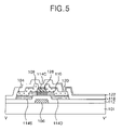
- FIG. 5 is a sectional view of the liquid crystal display panel taken along the line V–V′ in FIG. 4 ;
- FIGS. 6A and 6B show a plan view and a sectional view illustrating a first mask process according to the present invention
- FIGS. 7A and 7B show a plan view and a sectional view illustrating a process for forming an insulating pattern and an active layer according to the present invention
- FIGS. 8A to 8G are sectional views illustrating in detail a process for forming an insulating pattern and an active layer
- FIGS. 9A and 9B show a plan view and a sectional view illustrating in detail a second mask process according to the present invention
- FIGS. 10A to 10D are sectional views illustrating in detail the second mask process in FIG. 9 ;
- FIGS. 11A and 11B show a plan view and a sectional view illustrating a third mask process according to the present invention
- FIGS. 12A and 12B show a plan view and a sectional view illustrating a fourth mask process according to the present invention.
- FIGS. 13A to 13E are sectional views illustrating another fabricating process of a liquid crystal display panel having a polycrystalline silicon thin film transistor according to the present invention.
- FIG. 4 is a plan view of a liquid crystal display panel having a polycrystalline silicon thin film transistor according to a first embodiment of the present invention
- FIG. 5 is a sectional view of the liquid crystal display panel taken along the line V–V′ in FIG. 4 .
- a liquid crystal display panel includes a gate line 102 , a data line 104 crossing the gate line 102 with an insulating film 112 therebetween, a TFT 130 provided at a crossing of the gate line 102 and the data line 104 , and a pixel electrode 122 provided in a pixel area defined by the crossing of the gate line 102 and the data line 104 .
- the gate line 102 applies a gate signal to a gate electrode 106 of the TFT 130 .
- the data line 104 applies a pixel signal to the pixel electrode 122 via a drain electrode 110 of the TFT 130 .
- the TFT 130 includes the gate electrode 106 connected to the gate line 102 , a source electrode 108 connected to the data line 104 , and the drain electrode 110 connected to the pixel electrode 122 , via a contact hole 120 passing through a passivation film 118 .
- the gate electrode 106 is formed on a substrate 101 so as to overlap a channel area 114 C of an active layer, with the gate insulating film 112 between the gate electrode 106 and the channel area 114 C.
- the source electrode 108 is directly connected to a source area 114 S of the active layer and the drain electrode 110 is directly connected to a drain area 114 D of the active layer.
- An insulating pattern 128 is formed to overlap the channel area 114 C between the source electrode 108 and the drain electrode 110 .
- the insulting pattern 128 serves to prevent the channel area 114 C of the active layer from being over-etched.
- the active layer 114 is crystallized from an amorphous silicon film to a poly crystalline silicon film by a Field Enhanced Metal Induced Crystallization (FEMIC) method using a metal catalyst. Different ions, depending on the location of the active layer 114 and type of the TFT 130 , are injected into the active layer 114 . In other words, if the TFT 130 has an N channel, at least one of n + and n ⁇ ions is injected into the active layer. The active layer into which n ⁇ ions are injected becomes an LDD area, which is used to reduce the off-current of the TFT 130 .
- FEMIC Field Enhanced Metal Induced Crystallization
- the active layer into which n + ions are injected becomes the source area and the drain area, and the active layer into which the n + and n ⁇ ions are not injected becomes the channel area. If the TFT 130 has a P channel, p + ions are injected into the active layer. The active layer into which p + ions are injected becomes the source area and the drain area, and the portion of the active layer not injected with p + ions becomes the channel area.
- Such a TFT 130 responds to a scanning pulse applied from the gate line 102 to charge a video signal, that is, the pixel signal applied from the data line 104 in a liquid crystal cell. Accordingly, the liquid crystal cell controls a light transmittance in accordance with the charged pixel signal.
- an amorphous silicon film is transformed into a polycrystalline silicon film by FEMIC. Accordingly, an expensive laser equipment is not required for the crystallization, thereby increasing productivity.
- FIGS. 6A and 6B show a plan view and a sectional view illustrating in detail a first mask process according to the present invention.
- a first conductive patterning group including a gate electrode 106 and a gate line 102 is formed on a substrate 101 by a first mask process.
- a gate metal layer is entirely deposited on the lower substrate 101 by sputtering.
- the gate metal layer may be made of a metal including aluminum.
- the gate metal layer is patterned by a photolithography process and an etching process using the first mask, thereby forming the gate electrode 106 and the gate line 102 .
- a buffer layer may be formed between the first conductive patterning group and the lower substrate 101 .
- FIGS. 7A and 7B show a plan view and a sectional view illustrating in detail a process for forming an insulating pattern and a polycrystalline silicon layer according to the present invention.
- a gate insulating film 112 and a polycrystalline silicon film 114 are sequentially formed on the lower substrate 101 with the gate electrode 106 thereon, and an insulating pattern overlapping the gate electrode 106 is formed on the polycrystalline silicon film 114 .
- FIGS. 8A to 8G A detailed description will be made in conjunction with FIGS. 8A to 8G .
- a gate insulating film 112 such as silicon oxide (SiO 2 ) and an amorphous silicon film are sequentially formed on the lower substrate 101 having the first conductive patterning group thereon by a plasma enhanced chemical vapor deposition (PECVD).
- PECVD plasma enhanced chemical vapor deposition
- an insulating material 127 including, for example, silicon oxide (SiOx) or silicon nitride (SiNx), and a photo-resist film 170 are sequentially formed on the lower substrate 101 having the amorphous silicon film thereon. Then, as shown in FIG.
- the photo-resist film 170 is formed into a photo-resist pattern 172 by a backside-exposure process wherein a UV light is irradiated onto the photo-resist film 170 from the lower substrate 101 .
- the gate electrode 106 serves as a mask, and a developing process follows to form the photo-resist pattern 172 .
- an insulating pattern 128 is formed by etching the insulating material using the photo-resist pattern 172 as a mask, as shown in FIG. 8C .
- the insulating pattern 128 is formed to overlap the gate electrode 106 , with the gate insulating film 112 and the amorphous silicon film 124 therebetween.
- a derivative metal such as nickel (Ni) is deposited on the insulating pattern 128 and the amorphous silicon film 124 by sputtering or PECVD to crystallize the amorphous film 124 , as shown in FIG. 8D .
- the derivative metal is not formed on the portion of the amorphous silicon film 124 that is covered by the insulating pattern 128 .
- impurity ions corresponding to the type of the TFT 130 are injected into the amorphous silicon film 124 having the deposited derivative metal 140 .
- impurity ions corresponding to the type of the TFT 130 are injected into the amorphous silicon film 124 having the deposited derivative metal 140 .
- n + ions are injected, using the insulating pattern 128 as a mask, into the portion of the amorphous silicon film 124 that does not overlap the gate electrode 106 .
- p + ions are injected, using the insulating pattern 128 as a mask, into the portion of the amorphous silicon film 124 that does not overlap the gate electrode 106 .
- the amorphous film 124 having the derivative metal 140 deposited thereon is subjected to a heat treatment at a predetermined temperature and a predetermined electric field, as shown in FIG. 8F .
- the amorphous silicon film 124 A having the derivative metal 140 is crystallized by Metal Induced Crystallization (MIC)
- the amorphous silicon film 124 B without the induced metal 140 is crystallized by Metal Induced Lateral Crystallization (MILC) in which silicide formed by a reaction of the derivative metal 140 and the amorphous silicon film induces the crystallization of the amorphous silicon film, as the silicide continues to diffuse laterally in the amorphous silicon film 124 B.
- MILC Metal Induced Lateral Crystallization
- the heat treatment has a similar process condition to an annealing condition for activating the ions injected into the amorphous silicon film 124 , the crystallization process and an ion activation process are performed together at the same time.
- the amorphous silicon film is crystallized into a polycrystalline silicon film by the FEMIC, as shown in FIG. 8G , and the polycrystalline silicon film forms an active layer 114 divided into a source area 114 S, a channel area 114 C and a drain area 114 D depending on the ions injected into the polycrystalline silicon film.
- the channel area 114 C is the area overlapping the gate electrode 106
- the source area and the drain area are the areas excluding the channel area 114 C in the active layer 114 .
- the source area 114 S and the drain area 114 D of the active layer formed by a heat treatment are crystallized using the MIC method as the derivative metal is directly applied to those areas, and the channel area 114 C is crystallized by the MILC method.
- FIGS. 9A and 9B show a plan view and a sectional view illustrating in detail a second mask process according to the present invention.
- a second conductive patterning group including a data line 104 , a source electrode 108 and a drain electrode 110 of the TFT 130 , is formed on the lower substrate 101 with a second mask process, and an active layer 114 defining a source area 114 S and a drain area 114 D are also formed on the lower substrate 101 .
- a second mask process will be described in detail referring to FIGS. 10A to 10D .
- a data metal layer 109 is formed on the active layer 114 by a depositing method such as PECVD and sputtering.
- the data metal layer 109 may be made of chromium (Cr), copper (Cu), or molybdenum (Mo).
- the second mask 150 is formed of a transparent material and includes a mask substrate 152 whose exposed area becomes an exposing area S 2 , a shielding part 154 formed at a shielding area S 1 of the mask substrate 152 and a diffractive exposing part 156 (or a semi-transmitting part) formed at a partial exposing area S 3 of the mask substrate 152 .
- the photo-resist 158 is exposed and then developed using the second mask 150 , to thereby form a photo-resist pattern 160 having a stepped part between the shielding area S 1 and the partial exposing area S 3 corresponding to the shielding part 154 and the diffractive exposing part 156 as shown in FIG. 10B .
- the height of the photo-resist pattern 160 formed at the partial exposing area S 3 (second height) is lower than the height of the photo-resist pattern 160 formed at the shielding area S 1 (first height).
- the data metal layer is patterned by a wet etching process using the photo-resist pattern 160 as a mask, thereby forming a second conductive patterning group including the source and drain electrodes 108 and 110 in the TFT.
- the polycrystalline silicon film is patterned by a dry etching process using the photo-resist pattern 160 as a mask, thereby defining the source area 114 S and the drain area 114 D of the active layer.
- the photo-resist pattern 160 having the second height at the partial exposing area S 3 is removed by an ashing process using an oxygen (O 2 ) plasma, as shown in FIG. 10C , and the photo-resist pattern 160 having the first height at the shielding area S 1 has a lower height.
- the partial exposing area S 3 that is, the data metal layer overlapping the channel area of the TFT is removed by an etching process using the photo-resist pattern 160 .
- the integrated source and drain electrodes 108 and 110 are separated from each other, and thus the insulating pattern 128 overlapping the channel area 114 C is exposed. Then, the photo-resist pattern 160 remaining on the conductive patterning group is removed by a stripping process, as shown in FIG. 10D .
- FIGS. 11A and 11B show a plan view and a sectional view illustrating in detail a third mask process according to the present invention.
- a passivation film 118 having a contact hole 120 is formed on a lower substrate 101 having a second conductive patterning group formed thereon including a source electrode 108 and a drain electrode 110 with a third mask process.
- an insulating material is entirely deposited on the lower substrate 101 having the source electrode 108 and the drain electrode 110 formed thereon by a depositing method, such as PECVD and sputtering, thereby forming the passivation film 118 .
- the passivation film 118 is made of either an organic insulating material or an inorganic insulating material such as silicon oxide (SiO 2 ) and silicon nitride (SiNx).
- a photo-resist is deposited on the lower substrate 101 having the passivation film 118 formed thereon.
- the photo-resist is then patterned by a photolithography process using a third mask to form a photo-resist pattern.
- the passivation film 118 is patterned by an etching process using the photo-resist as a mask, thereby forming a contact hole 120 to expose the drain electrode 110 .
- FIGS. 12A and 12B show a plan view and a sectional view illustrating in detail a fourth mask process according to the present invention.
- a pixel electrode 122 to be located in a pixel region is formed on a lower substrate 101 having a passivation film 118 formed thereon using a fourth mask process.
- a transparent conductive material and a photo-resist are sequentially deposited on the lower substrate 101 having the passivation film 118 formed thereon by a depositing method such as sputtering.
- the transparent conductive material is made of any one of an indium-tin-oxide (ITO), an tin-oxide (TO) and an indium-zinc-oxide (IZO).
- the photo-resist is patterned by exposing and developing processes using a mask, thereby forming a photo-resist pattern.
- the transparent conductive material is patterned by an etching process using the photo-resist pattern as a mask, thereby forming a pixel electrode 122 .
- the pixel electrode 122 is connected to a drain electrode 110 of an N-type TFT located at a picture display panel via a contact hole 120 .
- FIGS. 13A to 13E are sectional views representing another fabricating method of a liquid crystal display panel having a polycrystalline silicon TFT according to the present invention.
- Another method of fabricating a liquid crystal display panel having a polycrystalline silicon TFT according to the present invention includes forming a gate pattern by the mask process in FIG. 6 ; forming an insulating pattern by a mask process in FIGS. 13A to 13E ; forming a data pattern and an active layer having an area defined by the mask process in FIG. 9 ; forming a passivation film having a contact hole by the mask process in FIG. 11 ; and forming a pixel electrode by the mask process in FIG. 12 .
- a gate insulating film 112 such as silicon oxide SiO 2 and an amorphous silicon film 124 are sequentially deposited on a lower substrate 101 having a gate electrode 106 formed thereon by using PECVD. Then, as shown in FIG. 13A , a derivative metal 140 such as nickel (Ni) is deposited on the amorphous silicon film 124 by sputtering and PECVD to crystallize the amorphous silicon film 124 .
- a derivative metal 140 such as nickel (Ni) is deposited on the amorphous silicon film 124 by sputtering and PECVD to crystallize the amorphous silicon film 124 .
- An insulating material including silicon oxide (SiOx) or silicon nitride (SiNx) is deposited on the lower substrate 101 having the derivative metal 140 by PECVD.
- the insulating material is patterned by photolithography and etching processes, thereby forming an insulating pattern 128 overlapping the gate electrode 106 as shown in FIG. 13B .
- Impurity ions corresponding to the type of the TFT 130 are injected into the amorphous silicon film having the insulating pattern 128 , as shown in FIG. 13C .
- n + ions are injected into the portion of the amorphous silicon film 124 that does not overlap the gate electrode 106 using the insulating pattern 128 as a mask.
- p + ions are injected into the amorphous silicon film 124 that does not overlap the gate electrode 106 using the insulating pattern 128 as a mask.
- the amorphous silicon film 124 having the derivative metal 140 deposited thereon is subjected to a heat treatment at a predetermined temperature and a predetermined electric field, as shown in FIG. 13D .
- the amorphous silicon film 124 to which the derivative metal 140 is applied is crystallized by a Metal Induced Crystallization (MIC) by the heat treatment.
- MIC Metal Induced Crystallization
- the heat treatment has a similar process condition to an annealing condition for activating the ions injected into the amorphous silicon film 124 , the crystallization process and an ion activation process are performed together at the same time.
- the derivative metal 140 within the active layer area overlapping the gate electrode 106 diffuses toward the backside of the substrate 101 by the heat treatment, and concentrates at the substrate 101 neighboring the impurity ions.
- the derivative metal does not remain within the area overlapping the gate electrode 106 by so-called gettering effect, thereby preventing a leakage current.
- the amorphous silicon film is crystallized into a polycrystalline silicon film by FEMIC, as shown in FIG. 13E , and the polycrystalline silicon film is divided into a source area 114 S, a channel area 114 C and a drain area 114 D depending on the ions injected into the polycrystalline silicon film.
- the source area 114 S and the drain area 114 D of the active layer formed by the heat treatment are crystallized by FEMIC as the derivative metal is directly applied to those areas.
- the ion injection process and the crystallization process are accomplished by the backside-exposure using the gate electrode as a mask, thereby forming the liquid crystal display panel using the four mask process.
- the number of masks and costs are reduced. Since the crystallization process is accomplished by FEMIC, an expensive laser equipment is not required, thereby increasing productivity.
Abstract
Description
Claims (7)
Priority Applications (1)
| Application Number | Priority Date | Filing Date | Title |
|---|---|---|---|
| US11/527,549 US7407841B2 (en) | 2003-06-28 | 2006-09-27 | Liquid crystal display panel and method of fabricating thereof |
Applications Claiming Priority (2)
| Application Number | Priority Date | Filing Date | Title |
|---|---|---|---|
| KR1020030042943A KR100928490B1 (en) | 2003-06-28 | 2003-06-28 | LCD panel and manufacturing method thereof |
| KR2003-42943 | 2003-06-28 |
Related Child Applications (1)
| Application Number | Title | Priority Date | Filing Date |
|---|---|---|---|
| US11/527,549 Division US7407841B2 (en) | 2003-06-28 | 2006-09-27 | Liquid crystal display panel and method of fabricating thereof |
Publications (2)
| Publication Number | Publication Date |
|---|---|
| US20040263707A1 US20040263707A1 (en) | 2004-12-30 |
| US7130002B2 true US7130002B2 (en) | 2006-10-31 |
Family
ID=33536359
Family Applications (2)
| Application Number | Title | Priority Date | Filing Date |
|---|---|---|---|
| US10/875,564 Active 2024-09-25 US7130002B2 (en) | 2003-06-28 | 2004-06-25 | LCD with metal diffused into the insulating layer over the channel area |
| US11/527,549 Active US7407841B2 (en) | 2003-06-28 | 2006-09-27 | Liquid crystal display panel and method of fabricating thereof |
Family Applications After (1)
| Application Number | Title | Priority Date | Filing Date |
|---|---|---|---|
| US11/527,549 Active US7407841B2 (en) | 2003-06-28 | 2006-09-27 | Liquid crystal display panel and method of fabricating thereof |
Country Status (2)
| Country | Link |
|---|---|
| US (2) | US7130002B2 (en) |
| KR (1) | KR100928490B1 (en) |
Cited By (8)
| Publication number | Priority date | Publication date | Assignee | Title |
|---|---|---|---|---|
| US20070153147A1 (en) * | 2005-12-30 | 2007-07-05 | Yi-Wei Lee | Method for manufacturing pixel structure |
| US20080296565A1 (en) * | 2007-05-31 | 2008-12-04 | Samsung Sdi Co., Ltd. | Method of fabricating polycrystalline silicon layer, tft fabricated using the same, method of fabricating tft, and organic light emitting diode display device having the same |
| US20090050894A1 (en) * | 2007-08-22 | 2009-02-26 | Samsung Sdi Co., Ltd. | Thin film transistor, method of fabricating the same, organic light emitting diode display device haing the tft, and method of fabricating the oled display device |
| US20090050893A1 (en) * | 2007-08-23 | 2009-02-26 | Samsung Sdi Co., Ltd. | Thin film transistor, method of fabricating the same, and organic light emitting diode display device including the same |
| US20090242895A1 (en) * | 2008-03-27 | 2009-10-01 | Samsung Mobile Display Co., Ltd. | Thin film transistor, method of fabricating the same, and organic lighting emitting diode display device including the same |
| US20090256469A1 (en) * | 2008-04-11 | 2009-10-15 | Samsung Mobile Display Co., Ltd. | Thin film transistor, method of fabricating the same and organic light emitting diode display device having the same |
| US20100006855A1 (en) * | 2008-07-14 | 2010-01-14 | Samsung Mobile Display Co., Ltd. | Thin film transistor, method of fabricating the same, and organic light emitting diode display device including the thin film transistor |
| CN102306709A (en) * | 2011-09-23 | 2012-01-04 | 北京大学 | Organic electroluminescent device and preparation method thereof |
Families Citing this family (9)
| Publication number | Priority date | Publication date | Assignee | Title |
|---|---|---|---|---|
| US7316784B2 (en) * | 2003-02-10 | 2008-01-08 | Lg.Philips Lcd Co., Ltd. | Method of patterning transparent conductive film, thin film transistor substrate using the same and fabricating method thereof |
| KR100863909B1 (en) * | 2007-04-06 | 2008-10-17 | 삼성에스디아이 주식회사 | A flat panel display device, and a method for manufacturing the same |
| KR100961757B1 (en) * | 2008-01-16 | 2010-06-07 | 서울대학교산학협력단 | Polycrystalline Silicon Solar Cell Having High Efficiency and Method for Fabricating the Same |
| KR100965778B1 (en) * | 2008-01-16 | 2010-06-24 | 서울대학교산학협력단 | Polycrystalline Silicon Solar Cell Having High Efficiency |
| CN102709184B (en) * | 2011-05-13 | 2016-08-17 | 京东方科技集团股份有限公司 | Thin film transistor (TFT), its manufacture method and array base palte containing polysilicon active layer |
| CN109417099A (en) * | 2016-04-25 | 2019-03-01 | 堺显示器制品株式会社 | Thin film transistor (TFT), display device and method for fabricating thin film transistor |
| CN109599343A (en) * | 2018-12-25 | 2019-04-09 | 惠科股份有限公司 | Thin film transistor and its manufacturing method |
| CN109742028B (en) * | 2018-12-25 | 2021-04-02 | 惠科股份有限公司 | Manufacturing method of thin film transistor, thin film transistor and display panel |
| CN109727875A (en) * | 2018-12-25 | 2019-05-07 | 惠科股份有限公司 | A kind of production method and display panel of thin film transistor (TFT) |
Citations (1)
| Publication number | Priority date | Publication date | Assignee | Title |
|---|---|---|---|---|
| US6617648B1 (en) * | 1998-02-25 | 2003-09-09 | Semiconductor Energy Laboratory Co., Ltd. | Projection TV |
Family Cites Families (17)
| Publication number | Priority date | Publication date | Assignee | Title |
|---|---|---|---|---|
| JP3255942B2 (en) * | 1991-06-19 | 2002-02-12 | 株式会社半導体エネルギー研究所 | Method for manufacturing inverted staggered thin film transistor |
| US6066547A (en) * | 1997-06-20 | 2000-05-23 | Sharp Laboratories Of America, Inc. | Thin-film transistor polycrystalline film formation by nickel induced, rapid thermal annealing method |
| JPH11111994A (en) * | 1997-10-03 | 1999-04-23 | Sanyo Electric Co Ltd | Thin-film transistor and method for manufacturing the thin-film transistor |
| US6228693B1 (en) * | 1998-06-05 | 2001-05-08 | Sharp Laboratories Of America, Inc. | Selected site, metal-induced, continuous crystallization method |
| US6346437B1 (en) * | 1998-07-16 | 2002-02-12 | Sharp Laboratories Of America, Inc. | Single crystal TFT from continuous transition metal delivery method |
| JP2000068513A (en) * | 1998-08-17 | 2000-03-03 | Sanyo Electric Co Ltd | Manufacture of semiconductor device |
| KR100325068B1 (en) * | 1998-08-27 | 2002-08-21 | 주식회사 현대 디스플레이 테크놀로지 | Manufacturing Method of Thin Film Transistor |
| KR100390522B1 (en) * | 2000-12-01 | 2003-07-07 | 피티플러스(주) | Method for fabricating thin film transistor including a crystalline silicone active layer |
| KR100650343B1 (en) * | 2000-12-29 | 2006-11-27 | 엘지.필립스 엘시디 주식회사 | Thin film transistor and the method of fabricating the same |
| US7439191B2 (en) * | 2002-04-05 | 2008-10-21 | Applied Materials, Inc. | Deposition of silicon layers for active matrix liquid crystal display (AMLCD) applications |
| KR100499371B1 (en) * | 2002-04-17 | 2005-07-04 | 엘지.필립스 엘시디 주식회사 | Thin film transistor array substrate and method of manufacturing the same |
| JP3612525B2 (en) * | 2002-06-04 | 2005-01-19 | Nec液晶テクノロジー株式会社 | Thin film semiconductor device manufacturing method and resist pattern forming method thereof |
| US20060049428A1 (en) * | 2002-07-05 | 2006-03-09 | Van Der Zaag Pieter J | Tft electronic devices and their manufacture |
| KR100869740B1 (en) * | 2002-08-17 | 2008-11-21 | 엘지디스플레이 주식회사 | Liquid Crystal Display Device and Fabricating Method Thereof |
| KR20040022770A (en) * | 2002-09-07 | 2004-03-18 | 엘지.필립스 엘시디 주식회사 | Method Of Fabricating Liquid Crystal Display Device |
| KR100886241B1 (en) * | 2002-09-10 | 2009-02-27 | 엘지디스플레이 주식회사 | Method Of Fabricating Liquid Crystal Display Device |
| US7316784B2 (en) * | 2003-02-10 | 2008-01-08 | Lg.Philips Lcd Co., Ltd. | Method of patterning transparent conductive film, thin film transistor substrate using the same and fabricating method thereof |
-
2003
- 2003-06-28 KR KR1020030042943A patent/KR100928490B1/en active IP Right Grant
-
2004
- 2004-06-25 US US10/875,564 patent/US7130002B2/en active Active
-
2006
- 2006-09-27 US US11/527,549 patent/US7407841B2/en active Active
Patent Citations (1)
| Publication number | Priority date | Publication date | Assignee | Title |
|---|---|---|---|---|
| US6617648B1 (en) * | 1998-02-25 | 2003-09-09 | Semiconductor Energy Laboratory Co., Ltd. | Projection TV |
Cited By (17)
| Publication number | Priority date | Publication date | Assignee | Title |
|---|---|---|---|---|
| US7580087B2 (en) * | 2005-12-30 | 2009-08-25 | Au Optronics Corp. | Method for manufacturing pixel structure |
| US20070153147A1 (en) * | 2005-12-30 | 2007-07-05 | Yi-Wei Lee | Method for manufacturing pixel structure |
| CN101315883B (en) * | 2007-05-31 | 2010-12-08 | 三星移动显示器株式会社 | Method of fabricating polycrystalline silicon layer, TFT fabricated using the same, method of fabricating TFT, and organic light emitting diode display device |
| US8790967B2 (en) | 2007-05-31 | 2014-07-29 | Samsung Display Co., Ltd. | Method of fabricating polycrystalline silicon layer, TFT fabricated using the same, method of fabricating TFT, and organic light emitting diode display device having the same |
| US20080296565A1 (en) * | 2007-05-31 | 2008-12-04 | Samsung Sdi Co., Ltd. | Method of fabricating polycrystalline silicon layer, tft fabricated using the same, method of fabricating tft, and organic light emitting diode display device having the same |
| US20090050894A1 (en) * | 2007-08-22 | 2009-02-26 | Samsung Sdi Co., Ltd. | Thin film transistor, method of fabricating the same, organic light emitting diode display device haing the tft, and method of fabricating the oled display device |
| US8513669B2 (en) | 2007-08-22 | 2013-08-20 | Samsung Display Co., Ltd. | Thin film transistor including metal or metal silicide structure in contact with semiconductor layer and organic light emitting diode display device having the thin film transistor |
| US8283668B2 (en) | 2007-08-23 | 2012-10-09 | Samsung Display Co., Ltd. | Thin film transistor, method of fabricating the same, and organic light emitting diode display device including the same |
| US20090050893A1 (en) * | 2007-08-23 | 2009-02-26 | Samsung Sdi Co., Ltd. | Thin film transistor, method of fabricating the same, and organic light emitting diode display device including the same |
| US20090242895A1 (en) * | 2008-03-27 | 2009-10-01 | Samsung Mobile Display Co., Ltd. | Thin film transistor, method of fabricating the same, and organic lighting emitting diode display device including the same |
| US8101952B2 (en) | 2008-03-27 | 2012-01-24 | Samsung Mobile Display Co., Ltd. | Thin film transistor, method of fabricating the same, and organic lighting emitting diode display device including the same |
| US8436360B2 (en) | 2008-03-27 | 2013-05-07 | Samsung Display Co., Ltd. | Thin film transistor, method of fabricating the same, and organic lighting emitting diode display device including the same |
| US20090256469A1 (en) * | 2008-04-11 | 2009-10-15 | Samsung Mobile Display Co., Ltd. | Thin film transistor, method of fabricating the same and organic light emitting diode display device having the same |
| US8318523B2 (en) | 2008-04-11 | 2012-11-27 | Samsung Display Co., Ltd. | Thin film transistor, method of fabricating the same and organic light emitting diode display device having the same |
| US8253141B2 (en) | 2008-07-14 | 2012-08-28 | Samsung Mobile Display Co., Ltd. | Thin film transistor, method of fabricating the same, and organic light emitting diode display device including the thin film transistor |
| US20100006855A1 (en) * | 2008-07-14 | 2010-01-14 | Samsung Mobile Display Co., Ltd. | Thin film transistor, method of fabricating the same, and organic light emitting diode display device including the thin film transistor |
| CN102306709A (en) * | 2011-09-23 | 2012-01-04 | 北京大学 | Organic electroluminescent device and preparation method thereof |
Also Published As
| Publication number | Publication date |
|---|---|
| US7407841B2 (en) | 2008-08-05 |
| US20040263707A1 (en) | 2004-12-30 |
| US20070019123A1 (en) | 2007-01-25 |
| KR20050001937A (en) | 2005-01-07 |
| KR100928490B1 (en) | 2009-11-26 |
Similar Documents
| Publication | Publication Date | Title |
|---|---|---|
| US7407841B2 (en) | Liquid crystal display panel and method of fabricating thereof | |
| EP2881785B1 (en) | Array substrate, manufacturing method therefor, and display apparatus | |
| US9735182B2 (en) | Array substrate, display device, and method for manufacturing the array substrate | |
| US7632722B2 (en) | Liquid crystal display device and method of fabricating the same | |
| US7300831B2 (en) | Liquid crystal display device having driving circuit and method of fabricating the same | |
| US8158469B2 (en) | Method of fabricating array substrate | |
| US8440483B2 (en) | Method of fabricating array substrate | |
| US8362526B2 (en) | Liquid crystal display device and fabricating method thereof | |
| US7612836B2 (en) | Liquid crystal display device and fabrication method thereof | |
| US6627471B2 (en) | Method of manufacturing an array substrate having drive integrated circuits | |
| US7344926B2 (en) | Liquid crystal display device and method of manufacturing the same | |
| US20060256251A1 (en) | Polycrystalline liquid crystal display device and method of fabricating the same | |
| US7206035B2 (en) | Method of fabricating liquid crystal display device | |
| KR100566612B1 (en) | Poly Silicon Thin Film Transistor and the fabrication method thereof | |
| US7348197B2 (en) | Liquid crystal display device and fabrication method thereof | |
| KR101265329B1 (en) | Thin film transistor and method for fabricating thereof and method for fabricating liquid crystal display device having thereof | |
| US7166501B2 (en) | Method for fabricating polycrystalline silicon liquid crystal display device | |
| US8018545B2 (en) | Method of fabricating a liquid crystal display device | |
| JPH06169086A (en) | Polycrystalline silicon thin film transistor | |
| KR101040490B1 (en) | Array substrate for LCD and the fabrication method thereof | |
| KR101086136B1 (en) | Fabrication method of liquid crystal display device | |
| KR20050066642A (en) | Fabrication method of liquid crystal display device | |
| KR20050064382A (en) | Fabrication method of liquid crystal display device | |
| JPH10274788A (en) | Manufacture of semiconductor device | |
| JP2000114542A (en) | Thin-film transistor and its manufacture |
Legal Events
| Date | Code | Title | Description |
|---|---|---|---|
| AS | Assignment |
Owner name: LG.PHILIPS LCD CO., LTD., KOREA, REPUBLIC OF Free format text: ASSIGNMENT OF ASSIGNORS INTEREST;ASSIGNORS:SEO, HYUN SIK;KIM, HAE YEOL;REEL/FRAME:015520/0790 Effective date: 20040624 |
|
| STCF | Information on status: patent grant |
Free format text: PATENTED CASE |
|
| AS | Assignment |
Owner name: LG DISPLAY CO., LTD., KOREA, REPUBLIC OF Free format text: CHANGE OF NAME;ASSIGNOR:LG.PHILIPS LCD CO., LTD.;REEL/FRAME:021754/0230 Effective date: 20080304 Owner name: LG DISPLAY CO., LTD.,KOREA, REPUBLIC OF Free format text: CHANGE OF NAME;ASSIGNOR:LG.PHILIPS LCD CO., LTD.;REEL/FRAME:021754/0230 Effective date: 20080304 |
|
| FEPP | Fee payment procedure |
Free format text: PAYER NUMBER DE-ASSIGNED (ORIGINAL EVENT CODE: RMPN); ENTITY STATUS OF PATENT OWNER: LARGE ENTITY Free format text: PAYOR NUMBER ASSIGNED (ORIGINAL EVENT CODE: ASPN); ENTITY STATUS OF PATENT OWNER: LARGE ENTITY |
|
| FPAY | Fee payment |
Year of fee payment: 4 |
|
| FPAY | Fee payment |
Year of fee payment: 8 |
|
| MAFP | Maintenance fee payment |
Free format text: PAYMENT OF MAINTENANCE FEE, 12TH YEAR, LARGE ENTITY (ORIGINAL EVENT CODE: M1553) Year of fee payment: 12 |