US7126147B2 - Storage phosphor readout system using resonant microcavity converter - Google Patents
Storage phosphor readout system using resonant microcavity converter Download PDFInfo
- Publication number
- US7126147B2 US7126147B2 US10/718,429 US71842903A US7126147B2 US 7126147 B2 US7126147 B2 US 7126147B2 US 71842903 A US71842903 A US 71842903A US 7126147 B2 US7126147 B2 US 7126147B2
- Authority
- US
- United States
- Prior art keywords
- converter
- emission
- light
- storage phosphor
- microcavity
- Prior art date
- Legal status (The legal status is an assumption and is not a legal conclusion. Google has not performed a legal analysis and makes no representation as to the accuracy of the status listed.)
- Expired - Fee Related, expires
Links
Images


Classifications
-
- G—PHYSICS
- G01—MEASURING; TESTING
- G01T—MEASUREMENT OF NUCLEAR OR X-RADIATION
- G01T1/00—Measuring X-radiation, gamma radiation, corpuscular radiation, or cosmic radiation
- G01T1/16—Measuring radiation intensity
- G01T1/20—Measuring radiation intensity with scintillation detectors
- G01T1/2012—Measuring radiation intensity with scintillation detectors using stimulable phosphors, e.g. stimulable phosphor sheets
- G01T1/2014—Reading out of stimulable sheets, e.g. latent image
Definitions
- This invention relates in general to a readout and detection system for storage phosphor screens used in radiographic imaging systems. More particularly, it relates to the inclusion in such a system of a device that converts electromagnetic radiation emitted from the screen in a wide angular distribution at one wavelength band into a narrower cone of emission at a longer wavelength band.
- Storage phosphor based radiographic imaging systems are currently in widespread use. These systems use screens containing phosphor material that store a portion of the incident ionizing radiation as latent storage sites. These sites are subsequently stimulated to release electromagnetic radiation (the stimulated emission), typically in the 350 to 450 nanometer range, in proportion to the amount of ionizing radiation that was absorbed by the phosphor material.
- the typical readout method used in these systems is the so-called flying-spot scanning method.
- a focused laser beam typically in the 600 to 700 nanometer range, is raster scanned over the surface of the screen to stimulate the storage sites. Synchronously, the stimulated emission is collected, detected, and digitized. The pixel size of the image is determined by the raster rate and digitization rate.
- the screens are flooded with erasing light to remove any remaining storage sites so the screen can be reused.
- the stimulated emission is emitted in a broad angular range.
- the emission is close to being Lambertian (a cos( ⁇ ) fall off in intensity with angle of emission).
- the typical collection systems have a large acceptance angle for the stimulated emission, and are highly reflective and shaped so that the emission is directed to a fairly large area detector, such as, a photomultiplier tube.
- the collector is a light-pipe, i.e., a plastic conduit that uses total internal reflection to guide the stimulated emission to the detector.
- the plastic must have a high transmittance for ultraviolet and blue electromagnetic radiation.
- the collection optics used must have a very low f-number to collect a large fraction of the emission. This places constraints on the depth of field of such an imaging system. Also, such low f-number optics can be more expensive than higher f-number optics. If the range of emission angles could be narrowed, the collection optics could be greatly simplified, thus saving space and cost.
- One such method of altering the emission angle range is disclosed in U.S. Pat. No. 6,507,032, issued Jan.
- the typical wavelength of the emission is 350 to 450 nanometers.
- the detector is typically a photomultiplier tube (PMT).
- the QE of a typical PMT has a value around 25% at 400 nanometers for a bi-alkali photocathode.
- typical CCD detectors have a QE at 400 nm that is typically 50% or lower. If the wavelength of the emission could be shifted towards longer wavelength, then CCD and other semiconductor detectors will detect the emission with higher QE.
- a storage phosphor imaging system comprising:
- a resonant microcavity converter for converting emitted radiation from said storage phosphor to radiation at a longer wavelength than said emitted radiation but with an angular intensity distribution that is substantially narrower than a Lambertian distribution;
- a detector for detecting said longer wavelength radiation.
- the invention has the following advantages.
- a storage phosphor readout system is provided that results in a narrower range of stimulated emission angles and shifts the wavelength to longer wavelengths where common semiconductor photodetectors have high QE.
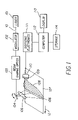
- FIG. 1 shows a schematic diagram of a storage phosphor readout system using the flying-spot method that includes an embodiment of resonant cavity converter according to the invention.
- FIG. 2 shows a cross-sectional view of the resonant cavity converter of FIG. 1 .
- FIG. 3A shows a side elevational view of a line-stimulation readout system incorporating a dichroic reflecting filter and a resonant cavity converter according to the invention with both stimulation and collection occurring along a direction approximately 90 degrees to the screen surface.
- FIG. 3B is a diagrammatic view which shows a more distant view schematically showing more than one stimulating and detecting unit across the width of the screen of FIG. 3A .
- FIG. 4 shows a side elevational view of a line-stimulation readout system using a resonant cavity converter of the invention with the stimulation occurring along a direction less than 90 degrees, and the collection occurring along a direction approximately 90 degrees to the screen without a dichroic reflecting filter.
- FIG. 5 shows a cross-sectional elevational view of a configuration with the resonant converter of the invention in intimate contact with the storage phosphor screen.
- the present invention provides for a storage phosphor readout system that results in a narrower range of stimulated emission angles and shifts the wavelength to longer wavelengths where common semiconductor photodetectors have high QE.
- the incorporation of a resonant microcavity device is used to perform this stimulated emission transformation.
- Laser 101 produces a laser beam 10 passed through an intensity modulator 102 for control of the laser exposure during the scan, e.g., turning off the laser during the retrace if a scanning galvonometer is used for laser beam steering.
- the laser beam 10 is then passed through beam shaping optics 103 that expand the beam to the desired size so subsequent focusing and steering optics 105 produce the desired spot size on the storage phosphor screen 107 .
- the laser beam is raster-scanned in a line scan across the screen 107 in the fast-scan direction by either a galvonometer scanner or a rotating polygon mirror 104 .
- the storage phosphor screen 107 is translated in the slow-scan direction 12 (perpendicular to the laser raster) at a rate such that the desired pixel size is obtained in the slow-scan direction.
- a resonant microcavity converter 106 is placed in close proximity to the storage phosphor screen 107 so that the laser beam 10 passes through it.
- the stimulated emission from the storage phosphor screen 107 is emitted with an intensity profile that is approximately Lambertian.
- the phosphor emission is absorbed by converter 106 and converted to an emission at a longer wavelength than the stimulated phosphor emission, but with an angular intensity distribution that is substantially narrower than Lambertian.
- a Lambertian distribution is one in which the intensity of emission per unit solid angle decreases as the cosine of the angle measured from the normal to the emitting surface.
- a Lambertian has a full-width-at-half-maximum (FWHM) of +/ ⁇ 60 degrees since the cosine of 60 degrees is 0.5.
- the converter 106 has an angular intensity distribution that is substantially less than Lambertian.
- the angular intensity distribution of the converter emission decreases faster than cosine of the emission angle.
- the preferred converters for this application have an angular intensity distribution with a FWHM that is less than or about +/ ⁇ 45 degrees, or more preferentially a FWHM that is less than or about +/ ⁇ 30 degrees.
- the converter emission is collected by the collector 108 and directed towards the filter 109 .
- This filter blocks the laser radiation from being sensed by the detector 110 , but passes the majority of the converter emission.
- the detector 110 senses the converter emission and provides a signal to the subsequent digitizing electronics 111 .
- the entire system is controlled by the computer 112 .
- the image data may be viewed on the display 113 , and stored in the storage device 114 .
- the converter 106 is a resonant microcavity device. Shown in FIG. 2 , is a cross-section of an exemplary configuration of such a converter. As shown, converter 106 includes substrate 210 that is transmissive to both the converter emission and the storage phosphor stimulation light. The substrate 210 may be transparent glass or plastic. On the substrate 210 is deposited a bottom dielectric stack 220 , which is composed of alternating high and low refractive index dielectric materials. The bottom dielectric stack 220 is designed to be reflective to the microcavity emission over a predetermined range of wavelengths, but transmissive to the storage phosphor stimulation wavelength. Typical high and low refractive index materials are TiO 2 and SiO 2 , respectively.
- the bottom dielectric stack 220 is deposited by standard electron-beam deposition, where a typical deposition temperature is 240° C.
- the organic active region 230 is deposited over the bottom dielectric stack 220 .
- the active region can be composed of small-molecular weight organic material, conjugated polymeric organic material, or a combination of the two.
- the small-molecular weight organic material is typically deposited by high vacuum (10 ⁇ 6 Torr) thermal evaporation, while the conjugated polymers are usually formed by spin casting.
- FIG. 2 shows the organic active region 230 is not a bulk layer but a multilayer composite.
- the organic active region 230 contains one or more organic periodic gain regions 260 , which are separated by spacer layers 270 .
- the thickness of the organic periodic gain regions 260 is typically less than 50 nm, with a preferred thickness of 5 to 25 nm.
- the thicknesses of the spacer layers 270 are chosen such that the organic periodic gain regions are aligned with the antinodes of the cavity's standing electromagnetic field.
- the active region 230 includes one or more organic periodic gain regions 260 and spacer layers 270 disposed on either side of the periodic gain region(s) and arranged so that the periodic gain region(s) is aligned with the antinodes of the device's standing wave electromagnetic field.
- the number of active periodic gain regions is chosen to obtain the desired absorption of the phosphor's stimulated emission.
- the number of periodic gain regions will typically be in the range of 2 to 10.
- An example of a useful host-dopant combination for green-emitting microcavities is aluminum tris(8-hydroxyquinoline) (Alq) as the host and [10-(2-benzothiazolyl)-2,3,6,7-tetrahydro-1,1,7,7-tetramethyl-1H,5H,11H-[1]Benzopyrano[6,7,8-ij]quinolizin-11-one] (C545T) as the dopant (at a volume fraction of 0.5%).
- Other host-dopant combinations can be used for emission in other wavelength regions, such as in the blue and red.
- organic periodic gain regions 260 can be composed of a single polymeric component, a blend of two or more polymeric materials, or a doped polymer or polymer blend.
- the gain media can also be a combination of more than one non-polymeric and polymeric materials with or without dopants. Typical dopants are listed previously for non-polymeric molecules. Non-polymeric dopants can be molecularly dispersed into the polymeric host, or the dopant could be added by copolymerizing a minor constituent into the host polymer.
- polymeric materials can be used such as poly(N-vinylcarbazole) (PVK), polythiophenes, polypyrrole, polyaniline, and copolymers such as poly(3,4-ethylenedioxythiophene)/poly(4-styrenesulfonate)also called PEDOT/PSS.
- PVK poly(N-vinylcarbazole)
- polythiophenes polythiophenes
- polypyrrole polypyrrole
- polyaniline polyaniline
- copolymers such as poly(3,4-ethylenedioxythiophene)/poly(4-styrenesulfonate) also called PEDOT/PSS.
- the spacer layer 270 it is preferred to use a material which is highly transparent to the microcavity emission 290 , the incident stimulated emission light 280 (produced by phosphor screen), and the laser light which stimulates the storage phosphor.
- an organic layer 1,1-Bis-(4-bis(4-methyl-phenyl)-amino-phenyl)-cyclohexane (TAPC), is chosen as the spacer material, since it has very low absorption throughout the visible and near UV spectrum and its index of refraction is slightly lower than that of Alq. This refractive index difference is useful since it helps in maximizing the overlap between the standing electric-field antinodes and the periodic gain regions 260 .
- Other useful spacer layer materials are inorganic compounds such at SiO 2 , which can be deposited thermally or electron-beam evaporation.
- the top dielectric stack 240 is deposited from the bottom dielectric stack 220 and reflective to light over a predetermined range of wavelengths. Its composition is analogous to that of the bottom dielectric stack 220 . Since the top dielectric stack 240 is deposited over an organic-based active region, its deposition temperature must be kept low in order to avoid melting the organics. As a result, a typical deposition temperature for the top dielectric stack 240 is 70° C. In order to obtain good emission efficiency, it is preferred that the peak reflectivity of the top dielectric stack 240 to the microcavity emission wavelength be greater than 99%, preferably greater than 99.9% in order to prevent microcavity light emission from exiting through it.
- the stack reflectance in order to enhance the out-coupling efficiency, it is preferred that the stack reflectance be smaller than 99%, where further reductions in the bottom stack reflectance result in higher external efficiencies, larger spectral linewidths, and larger microcavity light emission cone angles.
- the bottom dielectric stack 220 should be selected so that it's peak reflectance is less than 99%.
- the spectral linewidth is increased, thereby resulting in improved power conversion efficiency.
- the power conversion efficiency can be greater than 20%.
- the common storage phosphor materials used with a peak stimulated emission wavelength around 400 nm, and a green emitting microcavity this results in an external quantum conversion efficiency in excess of 30%.
- one or both of the exterior surfaces of the converter may have additional dielectric stack coatings to minimize reflection of the laser stimulating light so as to reduce flare, i.e., laser radiation hitting regions of the screen other than the desired pixel area.
- Collectors may be fabricated as light-pipe guides as disclosed in U.S. Pat. No. 5,138,161, issued Aug. 11, 1992, inventors Miyagawa et al. These light-pipe guides use total internal reflection to direct the emission to the detector 110 , so the light propagates within the light-guide material.
- the common phosphor material used in storage phosphor screen 107 is a barium fluorohalide doped with europium.
- the microcavity converter 106 is placed in close proximity to the storage phosphor screen 107 , the spacing from the top of the storage phosphor screen 107 being in the range of 0.025 to 0.5 mm, preferably in the range of 0.025 to 0.1 mm.
- the stimulated emission from the storage phosphor screen 107 is absorbed by the converter 106 and re-emitted by the converter 106 at a longer wavelength than the stimulated emission and in an intensity profile that is much narrower than a Lambertian.
- the converter emission is reflected by the dichroic filter 303 and directed towards at least one imaging lens(es) 304 that in turn focus an image of the emission onto the corresponding segmented detector(s) 305 .
- the microcavity converter 106 covers, and is in intimate contact with but not optically coupled to, the storage phosphor screen 107 .
- the different geometrical configurations for reading out the storage phosphor screen as shown in FIG. 1 , FIG. 3A and FIG. 4 can still be used, but the converter is now covering the entire screen.
- the advantage here is mainly for the re-imaging of the line stimulation configuration of FIG. 3A and FIG. 4 . With the intimate but not optical contact between the screen and the converter, there is no loss in resolution of the re-imaged converter emission since there is no gap between the screen and the converter.
Abstract
Description
- 10 laser beam
- 12 slow-scan direction
- 101 laser
- 102 modulator
- 103 beam shaping optics
- 104 rotating polygon mirror
- 105 steering optics
- 106 microcavity converter
- 107 storage phosphor screen
- 108 light collector
- 109 filter
- 110 detector
- 111 digitizing electronics
- 112 computer
- 113 display
- 114 storage device
- 210 substrate
- 220 bottom dielectric stack
- 230 organic active region
- 240 top dielectric stack
- 260 organic periodic gain regions
- 270 spacer layers
- 280 stimulated emission light
- 290 microcavity emission
- 300 multiple stimulating and detecting subsystems
- 301 stimulating light source
- 302 imaging lenses
- 303 dichroic filter
- 304 imaging lenses
- 305 segmented detectors
- 306 imaging processing system
- 309 filter
- 330 mirror
Claims (13)
Priority Applications (4)
| Application Number | Priority Date | Filing Date | Title |
|---|---|---|---|
| US10/718,429 US7126147B2 (en) | 2003-11-20 | 2003-11-20 | Storage phosphor readout system using resonant microcavity converter |
| PCT/US2004/034722 WO2005057236A2 (en) | 2003-11-20 | 2004-10-20 | Storage phosphor system using resonant microcavity converter |
| CN200480034253.5A CN1882851A (en) | 2003-11-20 | 2004-10-20 | Storage phosphor readout system using resonant microcavity converter |
| JP2006541170A JP2007524848A (en) | 2003-11-20 | 2004-10-20 | Memory phosphor system using a resonant microcavity converter |
Applications Claiming Priority (1)
| Application Number | Priority Date | Filing Date | Title |
|---|---|---|---|
| US10/718,429 US7126147B2 (en) | 2003-11-20 | 2003-11-20 | Storage phosphor readout system using resonant microcavity converter |
Publications (2)
| Publication Number | Publication Date |
|---|---|
| US20050109962A1 US20050109962A1 (en) | 2005-05-26 |
| US7126147B2 true US7126147B2 (en) | 2006-10-24 |
Family
ID=34591097
Family Applications (1)
| Application Number | Title | Priority Date | Filing Date |
|---|---|---|---|
| US10/718,429 Expired - Fee Related US7126147B2 (en) | 2003-11-20 | 2003-11-20 | Storage phosphor readout system using resonant microcavity converter |
Country Status (4)
| Country | Link |
|---|---|
| US (1) | US7126147B2 (en) |
| JP (1) | JP2007524848A (en) |
| CN (1) | CN1882851A (en) |
| WO (1) | WO2005057236A2 (en) |
Cited By (3)
| Publication number | Priority date | Publication date | Assignee | Title |
|---|---|---|---|---|
| US20060071186A1 (en) * | 2004-10-01 | 2006-04-06 | Fuji Photo Film Co., Ltd. | Image readout apparatus |
| US20140264078A1 (en) * | 2013-03-12 | 2014-09-18 | Agfa Healthcare Nv | Radiation Image Read-Out and Cropping System |
| CN108351427A (en) * | 2015-09-09 | 2018-07-31 | 诺基亚技术有限公司 | The method of the device of device and offer for detecting radiation for detecting radiation |
Families Citing this family (3)
| Publication number | Priority date | Publication date | Assignee | Title |
|---|---|---|---|---|
| US7244955B2 (en) * | 2005-12-15 | 2007-07-17 | General Electric Company | Computed radiography systems and methods of use |
| DE102007045799B4 (en) * | 2007-09-25 | 2016-02-18 | Fraunhofer-Gesellschaft zur Förderung der angewandten Forschung e.V. | Modular X-ray image X-ray detector and X-ray detection method |
| CN113125471B (en) * | 2021-03-31 | 2023-06-27 | 武汉联影生命科学仪器有限公司 | Scanning system and scanning control method |
Citations (11)
| Publication number | Priority date | Publication date | Assignee | Title |
|---|---|---|---|---|
| US4800276A (en) * | 1984-08-17 | 1989-01-24 | Fuji Photo Film Co., Ltd. | Radiation image read-out apparatus |
| US4881236A (en) | 1988-04-22 | 1989-11-14 | University Of New Mexico | Wavelength-resonant surface-emitting semiconductor laser |
| US5138161A (en) | 1990-04-20 | 1992-08-11 | Fuji Photo Film Co., Ltd. | Apparatus for reading radiation image information |
| US5881083A (en) | 1997-07-03 | 1999-03-09 | The Regents Of The University Of California | Conjugated polymers as materials for solid state laser |
| EP1103846A1 (en) | 1999-11-23 | 2001-05-30 | Agfa-Gevaert N.V. | Storage phosphor panel with increased luminous efficiency |
| US20020008212A1 (en) | 2000-07-18 | 2002-01-24 | Fuji Photo Film Co., Ltd. | Apparatus for reading radiation image information |
| US6373074B1 (en) | 1997-11-28 | 2002-04-16 | Agfa-Fevaert Aktiengesellschaft | Device for reading out information stored in a phosphor-carrier, and an x-ray cassette |
| US6392341B2 (en) * | 1993-07-20 | 2002-05-21 | University Of Georgia Research Foundation, Inc. | Resonant microcavity display with a light distribution element |
| US20030075720A1 (en) * | 2001-09-28 | 2003-04-24 | Eastman Kodak Company | Organic light-emitting diode having an interface layer between the hole-transporting layer and the light-emitting layer |
| US20030132395A1 (en) * | 2000-06-29 | 2003-07-17 | Essex Electro Engineers, Inc. | Method and apparatus for radiographic imaging |
| US6644792B1 (en) | 2002-10-25 | 2003-11-11 | Eastman Kodak Company | Ink droplet forming apparatus and method for use in ink jet printer system |
Family Cites Families (1)
| Publication number | Priority date | Publication date | Assignee | Title |
|---|---|---|---|---|
| US5881161A (en) * | 1998-06-17 | 1999-03-09 | Merry Electronics Co., Ltd. | Headphone |
-
2003
- 2003-11-20 US US10/718,429 patent/US7126147B2/en not_active Expired - Fee Related
-
2004
- 2004-10-20 WO PCT/US2004/034722 patent/WO2005057236A2/en active Application Filing
- 2004-10-20 JP JP2006541170A patent/JP2007524848A/en not_active Withdrawn
- 2004-10-20 CN CN200480034253.5A patent/CN1882851A/en active Pending
Patent Citations (12)
| Publication number | Priority date | Publication date | Assignee | Title |
|---|---|---|---|---|
| US4800276A (en) * | 1984-08-17 | 1989-01-24 | Fuji Photo Film Co., Ltd. | Radiation image read-out apparatus |
| US4881236A (en) | 1988-04-22 | 1989-11-14 | University Of New Mexico | Wavelength-resonant surface-emitting semiconductor laser |
| US5138161A (en) | 1990-04-20 | 1992-08-11 | Fuji Photo Film Co., Ltd. | Apparatus for reading radiation image information |
| US6392341B2 (en) * | 1993-07-20 | 2002-05-21 | University Of Georgia Research Foundation, Inc. | Resonant microcavity display with a light distribution element |
| US5881083A (en) | 1997-07-03 | 1999-03-09 | The Regents Of The University Of California | Conjugated polymers as materials for solid state laser |
| US6373074B1 (en) | 1997-11-28 | 2002-04-16 | Agfa-Fevaert Aktiengesellschaft | Device for reading out information stored in a phosphor-carrier, and an x-ray cassette |
| EP1103846A1 (en) | 1999-11-23 | 2001-05-30 | Agfa-Gevaert N.V. | Storage phosphor panel with increased luminous efficiency |
| US6507032B1 (en) * | 1999-11-23 | 2003-01-14 | Agfa-Gevaert | Storage phosphor panel with increased luminous efficiency |
| US20030132395A1 (en) * | 2000-06-29 | 2003-07-17 | Essex Electro Engineers, Inc. | Method and apparatus for radiographic imaging |
| US20020008212A1 (en) | 2000-07-18 | 2002-01-24 | Fuji Photo Film Co., Ltd. | Apparatus for reading radiation image information |
| US20030075720A1 (en) * | 2001-09-28 | 2003-04-24 | Eastman Kodak Company | Organic light-emitting diode having an interface layer between the hole-transporting layer and the light-emitting layer |
| US6644792B1 (en) | 2002-10-25 | 2003-11-11 | Eastman Kodak Company | Ink droplet forming apparatus and method for use in ink jet printer system |
Non-Patent Citations (3)
| Title |
|---|
| Applied Physics Letters, vol. 72, No. 11, Mar. 1998, H. Becker et al., Light emission from wavelength-tunable microcavities, pp. 1266-1268. |
| M. Berggren et al., Light amplification in organic thin films using cascade energy transfer, Nature, vol. 389 389, pp. 466-469, Oct. 1997. |
| Owen et al., Progress toward prototype high-definition video-projection CRTs using resonant microcavity phosphor display technology, Sep. 2003, Proceedings of SPIE, vol. 5080, pp. 218-225. * |
Cited By (4)
| Publication number | Priority date | Publication date | Assignee | Title |
|---|---|---|---|---|
| US20060071186A1 (en) * | 2004-10-01 | 2006-04-06 | Fuji Photo Film Co., Ltd. | Image readout apparatus |
| US20140264078A1 (en) * | 2013-03-12 | 2014-09-18 | Agfa Healthcare Nv | Radiation Image Read-Out and Cropping System |
| CN108351427A (en) * | 2015-09-09 | 2018-07-31 | 诺基亚技术有限公司 | The method of the device of device and offer for detecting radiation for detecting radiation |
| CN108351427B (en) * | 2015-09-09 | 2021-07-16 | 诺基亚技术有限公司 | Device for detecting radiation and method for providing a device for detecting radiation |
Also Published As
| Publication number | Publication date |
|---|---|
| JP2007524848A (en) | 2007-08-30 |
| WO2005057236A2 (en) | 2005-06-23 |
| WO2005057236A3 (en) | 2005-07-14 |
| CN1882851A (en) | 2006-12-20 |
| US20050109962A1 (en) | 2005-05-26 |
Similar Documents
| Publication | Publication Date | Title |
|---|---|---|
| EP1333550B1 (en) | Organic vertical cavity phase-locked laser array device | |
| US6160273A (en) | Diode pumped solid state edge emitting light source | |
| US6853660B2 (en) | Organic laser cavity arrays | |
| EP1359752B1 (en) | Scanned display systems using color laser light sources | |
| US6064069A (en) | Solid state camera element | |
| EP1365490B1 (en) | Organic vertical cavity phase-locked laser array device | |
| US8203155B2 (en) | Cavity-enhanced multispectral photonic devices | |
| US7126147B2 (en) | Storage phosphor readout system using resonant microcavity converter | |
| KR101009868B1 (en) | Vertical cavity light-producing device with improved power conversion | |
| US20220006268A1 (en) | Light-emitting device, optical device, and information processing device | |
| JPH0645650A (en) | Semiconductor light emittng element and optical detector, optical information processing device, and light emitting device using it | |
| US6818913B2 (en) | Method and apparatus for reading image information by use of stimulable phosphor, and solid-state image detector | |
| US20040076202A1 (en) | Organic laser that is attachable to an external pump beam light source | |
| US5822501A (en) | Optical scanning device having dichroic mirror for separating reading and recording light beams | |
| US20230123994A1 (en) | Spatial light modulators, methods of driving and manufacturing the same, and apparatuses including the spatial light modulators | |
| US20010042823A1 (en) | Radiation image read-out apparatus | |
| EP2034511B1 (en) | Illuminating light source, scanner module employing the same, and image scanning apparatus employing the scanner module | |
| JP2001201809A (en) | Radiographic image reader | |
| KR100338027B1 (en) | Beam index type cathode ray tube | |
| KR20220167779A (en) | Optical sensor package and array apparatus | |
| CN1497801A (en) | Organic laser capable of connecting external excitation beam source | |
| CN1497811A (en) | Organic laser cavity array | |
| JPH09197584A (en) | Light guide used for radiation image reader |
Legal Events
| Date | Code | Title | Description |
|---|---|---|---|
| AS | Assignment |
Owner name: EASTMAN KODAK COMPANY, NEW YORK Free format text: ASSIGNMENT OF ASSIGNORS INTEREST;ASSIGNORS:TRAUERNICHT, DAVID P.;KAHEN, KEITH B.;REEL/FRAME:014746/0664;SIGNING DATES FROM 20031118 TO 20031120 |
|
| FEPP | Fee payment procedure |
Free format text: PAYOR NUMBER ASSIGNED (ORIGINAL EVENT CODE: ASPN); ENTITY STATUS OF PATENT OWNER: LARGE ENTITY |
|
| AS | Assignment |
Owner name: CARESTREAM HEALTH, INC., NEW YORK Free format text: ASSIGNMENT OF ASSIGNORS INTEREST;ASSIGNOR:EASTMAN KODAK COMPANY;REEL/FRAME:020741/0126 Effective date: 20070501 Owner name: CARESTREAM HEALTH, INC., NEW YORK Free format text: ASSIGNMENT OF ASSIGNORS INTEREST;ASSIGNOR:EASTMAN KODAK COMPANY;REEL/FRAME:020756/0500 Effective date: 20070501 Owner name: CARESTREAM HEALTH, INC.,NEW YORK Free format text: ASSIGNMENT OF ASSIGNORS INTEREST;ASSIGNOR:EASTMAN KODAK COMPANY;REEL/FRAME:020741/0126 Effective date: 20070501 Owner name: CARESTREAM HEALTH, INC.,NEW YORK Free format text: ASSIGNMENT OF ASSIGNORS INTEREST;ASSIGNOR:EASTMAN KODAK COMPANY;REEL/FRAME:020756/0500 Effective date: 20070501 |
|
| REMI | Maintenance fee reminder mailed | ||
| LAPS | Lapse for failure to pay maintenance fees | ||
| STCH | Information on status: patent discontinuation |
Free format text: PATENT EXPIRED DUE TO NONPAYMENT OF MAINTENANCE FEES UNDER 37 CFR 1.362 |
|
| FP | Lapsed due to failure to pay maintenance fee |
Effective date: 20101024 |