US7088748B2 - Tunable laser - Google Patents
Tunable laser Download PDFInfo
- Publication number
- US7088748B2 US7088748B2 US10/472,254 US47225403A US7088748B2 US 7088748 B2 US7088748 B2 US 7088748B2 US 47225403 A US47225403 A US 47225403A US 7088748 B2 US7088748 B2 US 7088748B2
- Authority
- US
- United States
- Prior art keywords
- grating
- grating unit
- tuneable laser
- units
- unit
- Prior art date
- Legal status (The legal status is an assumption and is not a legal conclusion. Google has not performed a legal analysis and makes no representation as to the accuracy of the status listed.)
- Expired - Lifetime, expires
Links
Images


Classifications
-
- H—ELECTRICITY
- H01—ELECTRIC ELEMENTS
- H01S—DEVICES USING THE PROCESS OF LIGHT AMPLIFICATION BY STIMULATED EMISSION OF RADIATION [LASER] TO AMPLIFY OR GENERATE LIGHT; DEVICES USING STIMULATED EMISSION OF ELECTROMAGNETIC RADIATION IN WAVE RANGES OTHER THAN OPTICAL
- H01S5/00—Semiconductor lasers
- H01S5/06—Arrangements for controlling the laser output parameters, e.g. by operating on the active medium
- H01S5/062—Arrangements for controlling the laser output parameters, e.g. by operating on the active medium by varying the potential of the electrodes
- H01S5/0625—Arrangements for controlling the laser output parameters, e.g. by operating on the active medium by varying the potential of the electrodes in multi-section lasers
- H01S5/06255—Controlling the frequency of the radiation
- H01S5/06256—Controlling the frequency of the radiation with DBR-structure
-
- H—ELECTRICITY
- H01—ELECTRIC ELEMENTS
- H01S—DEVICES USING THE PROCESS OF LIGHT AMPLIFICATION BY STIMULATED EMISSION OF RADIATION [LASER] TO AMPLIFY OR GENERATE LIGHT; DEVICES USING STIMULATED EMISSION OF ELECTROMAGNETIC RADIATION IN WAVE RANGES OTHER THAN OPTICAL
- H01S5/00—Semiconductor lasers
- H01S5/10—Construction or shape of the optical resonator, e.g. extended or external cavity, coupled cavities, bent-guide, varying width, thickness or composition of the active region
- H01S5/12—Construction or shape of the optical resonator, e.g. extended or external cavity, coupled cavities, bent-guide, varying width, thickness or composition of the active region the resonator having a periodic structure, e.g. in distributed feedback [DFB] lasers
- H01S5/1206—Construction or shape of the optical resonator, e.g. extended or external cavity, coupled cavities, bent-guide, varying width, thickness or composition of the active region the resonator having a periodic structure, e.g. in distributed feedback [DFB] lasers having a non constant or multiplicity of periods
- H01S5/1215—Multiplicity of periods
Definitions
- the invention relates to a tuneable laser, in particular but not exclusively to a three section distributed Bragg reflector tuneable laser.
- Tuneable lasers are well known in the field of optical communications, particularly in connection with wavelength divisional multiplex telecommunication systems, which rely upon either being fed by stacks of individually wavelength distributed Bragg reflectors (DBR) lasers, which can be individually selected, or by a wide tuning range tuneable laser that can be electronically driven to provide the wavelength required.
- DBR distributed Bragg reflectors
- Limited tuning range tuneable lasers that rely upon thermal effects for tuning are also available.
- U.S. Pat. No. 4,896,325 discloses a wavelength tuneable laser having sampled gratings at the front and rear of its gain region.
- the gratings produce slightly different reflection combs which provide feedback into the device.
- the gratings can be current tuned in wavelength with respect to each other.
- Co-incidence of a maximum from each of the front and rear gratings is referred to as a supermode.
- To switch the device between super modes requires a small electrical current into one of the gratings to cause a different pair of maxima to co-incide in the manner of a vemier.
- continuous tuning within a supermode can be achieved.
- the reflection spectra of the known sampled grating structures have a Gaussian type envelope which limits the total optical bandwidth over which the laser can reliably operate as a single mode device.
- each grating unit comprises a series of adjacent gratings having the same pitch, which gratings are separated by a phase change of ⁇ radians, wherein the gratings have different lengths to provide a pre-determined reflection spectrum.
- the known devices have Bragg gratings which bound both ends of the gain and phase regions of a four section tuneable laser, which produces a comb wavelength response.
- For a given set of drive currents in the front and rear grating sections there is simultaneous correspondence in reflection peak at only one wavelength, as a consequence of which the device lases at that wavelength.
- To change this wavelength a different current is applied to the front and rear gratings.
- the front and rear gratings operate in a vernier mode, in which the wavelengths of correspondence determine a supermode wavelength.
- the known devices have generally been acceptable, they share a tendency to suffer from short wavelength losses, which in combination with the front grating tuning absorption reduces the output power of the laser.
- the present invention seeks to provide a tuneable laser with a higher optical output power whilst having acceptable manufacturing costs.
- a tuneable laser having an active section, a phase section and a Bragg reflector comprising a plurality of discrete grating units, wherein at least one grating unit has at least two independently actuable electrodes and in which at least two of the grating units have different pitches.
- the desired wavelength of the laser can be selected by applying an electric current to only one of the electrodes associated with each grating associated with a particular wavelength.
- the refractive index in the region of the grating under the said electrode will locally decrease the refractive index. This results in the individual reflection peak in the reflection comb being split.
- this latter wavelength becomes the pre-dominant wavelength at which the device will lase. This wavelength can then be current controlled in the known manner.
- the tuneable laser is provided with a simple partial reflecting front mirror.
- the Bragg reflector comprises three or more, preferably six, discrete grating units each having a discrete pitch.
- the pitch of the gratings increases with distance from the gain region.
- each grating unit is provided with two independently actuable electrodes.
- a conventional switching circuit is provided to switch the current to the electrodes and grating units.
- the tuneable laser of the invention has a number of advantages over the known designs, in particular minimising the short wavelength losses inherent in the four section DBR lasers of the prior art, thereby having higher power output.
- absorption losses are minimised as there is no contribution to tuning induced absorption from the front Bragg reflector, which usually dominates absorption.
- the absorption losses due to tuning in the Bragg reflector is reduced than in known SG-DBR lasers as the use of a shorter grating is facilitated.
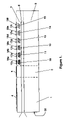
- FIG. 1 shows a schematic representation of a three section laser according to a first embodiment
- FIG. 2 shows a schematic representation of the Bragg reflector of FIG. 1 ;
- FIG. 3 a shows a wavelength envelope using a known Bragg reflector
- FIG. 3 b shows a wavelength envelope using the Bragg reflector of FIG. 1 ;
- FIG. 4 shows a second embodiment
- FIG. 1 shows a schematic three section tuneable DBR semiconductor laser having an active or gain section 1 , a phase section 2 and a rear mirror section 3 . Both the gain section 1 and the phase section 2 are provided with electrodes 4 , 5 . At the boundary of the gain section 1 , a front mirror 20 is provided, which mirror can be a simple partial reflecting mirror or other suitable mirror.
- the laser further comprises an active region 6 , the Bragg reflector layer 7 and substrate layer 8 .
- the rear mirror section 3 has a plurality of discrete Bragg grating units 10 – 15 etched into the waveguide, each of which has a discrete pitch corresponding to a desired wavelength.
- Each of the grating units 10 – 15 is spatially separated from the adjacent grating unit.
- each grating unit is provided with two electrodes 17 a–f , 18 a–f , which are adapted to be independently actuable from one another and the other electrodes in the rear mirror section.
- FIG. 2 shows a schematic representation of a Bragg reflector forming the rear mirror section 3 .
- the Bragg reflector comprises a plurality, in this case six, of discrete grating units 10 – 15 , each having a discrete pitch.
- the grating unit closest to the phase section 2 has the shortest pitch and the pitch of each successive grating unit remote from the phase section is greater than the pitch of the preceding unit.
- Two electrodes 17 a–f , 18 a–f are associated with each grating unit 10 – 15 , which electrodes are independently actuable of one another.
- the Bragg gratings can be fabricated using electron beam writing techniques or phase mask holographic techniques.
- a grating unit corresponding to a particular desired wavelength is selected (e.g. 13 ) and current is applied to both electrodes ( 17 d , 18 d ).
- This has the effect of lowering the effective refractive index of the grating and therefore the Bragg wavelength of the grating.
- the effective refractive index of a part of the grating will be changed but the remaining part will remain unchanged as the current will only spread slightly through the layer in which the grating is etched.
- This has the effect that the reflection maxima for that particular grating is split into two maxima having a maximum intensity of about half the previous maxima at slightly different wavelengths. If this is undertaken at all of the gratings except the grating corresponding to the desired wavelength, then this latter wavelength becomes the dominant wavelength in the active cavity. The laser will therefore lase at this wavelength, which can then be current tuned.
- the laser can be current tuned across the reflection spectrum by a combination of desired grating selection and control of the current to said desired grating.
- the grating corresponding to the desired wavelength has equal current driven into each of its grating unit electrodes, wherein the current is varied to tune the wavelength down to its next adjacent grating wavelength.
- FIG. 3 a shows the typical reflection spectrum obtained using a prior art phase shifted Bragg reflector such as is known from GB 2337135.
- a prior art phase shifted Bragg reflector such as is known from GB 2337135.
- Such a reflector has a number of discrete reflection peaks, which are of substantially similar intensities. These peaks are generally separated by about 7 nm for a C-Band or L-Band device and a device incorporating such a reflector can be tuned to lase in the known manner by causing superposition of the individual modes.
- the reflector of the invention has a similar reflection spectrum to that in shown in FIG. 3 a , when no current is applied to the electrodes associated with the grating units. However, when current is applied to one of each electrodes in the manner described in relation to FIG. 2 and to both electrodes of the grating unit associated with the desired wavelength, a spectrum is obtained as shown in FIG. 3 b . In this case, each of the reflection peaks 51 , 52 , 53 , 55 and 56 has been split into two equal reflection peaks having approximately half the intensity of the remaining reflection peak 54 . It is at the wavelength of the remaining reflection peak 54 that the device will lase.
- a mirror section 102 and a non-selective front mirror 103 define the lasing cavity.
- the mirror section 102 has three Bragg grating sections 104 , 105 and 106 .
- Each section has a Bragg grating 104 a , 105 a and 106 a which has a constant pitch with pitch 105 a being larger than 104 a but smaller than 105 a .
- Each section 104 to 106 has a pair of electrodes 104 b , 104 c etc which operate in the manner described above with reference to FIGS. 1 and 2 .
- phase shift will be controlled using the phase section in a conventional manner. It would, however, be possible to control the phase by selectively applying current to the electrodes located between the reflecting grating and the active section.
- the front mirror is preferably a simple partial reflecting mirror, it can be any suitable mirror which will have the same reflection spectrum as the rear mirror. Whilst a simple mirror will minimise losses, a Bragg grating could also be used.
- the invention design may be suitably applied to solid state lasers manufactured using Group III-V or other semiconductor materials.
- the photoluminescent gain curve of semiconductor materials is curved with intensity falloff at the edges of the spectrum.
- the Bragg grating unit lengths can be varied to give enhanced reflectivity where required.
- the reflectively profile of a grating can be controlled such that the reflection peach has a sharp definition at the wavelength of interest thereby giving good side mode suppression.
- An example of such a grating is one that has along each its length a Gaussian or Lorentzian reflectively profile.
Applications Claiming Priority (3)
| Application Number | Priority Date | Filing Date | Title |
|---|---|---|---|
| GB0106791A GB2373632B (en) | 2001-03-19 | 2001-03-19 | Tuneable laser |
| GB0106791.7 | 2001-03-19 | ||
| PCT/GB2002/001170 WO2002075875A2 (fr) | 2001-03-19 | 2002-03-14 | Laser accordable |
Publications (2)
| Publication Number | Publication Date |
|---|---|
| US20040081211A1 US20040081211A1 (en) | 2004-04-29 |
| US7088748B2 true US7088748B2 (en) | 2006-08-08 |
Family
ID=9911029
Family Applications (1)
| Application Number | Title | Priority Date | Filing Date |
|---|---|---|---|
| US10/472,254 Expired - Lifetime US7088748B2 (en) | 2001-03-19 | 2002-03-14 | Tunable laser |
Country Status (4)
| Country | Link |
|---|---|
| US (1) | US7088748B2 (fr) |
| AU (1) | AU2002241096A1 (fr) |
| GB (1) | GB2373632B (fr) |
| WO (1) | WO2002075875A2 (fr) |
Families Citing this family (3)
| Publication number | Priority date | Publication date | Assignee | Title |
|---|---|---|---|---|
| GB2378036A (en) * | 2001-04-30 | 2003-01-29 | Jds Uniphase Corp | Multi-wavelength switchable laser system |
| US9997890B2 (en) | 2015-10-28 | 2018-06-12 | Rockley Photonics Limited | Discrete wavelength tunable laser |
| US9627851B1 (en) | 2015-10-28 | 2017-04-18 | Rockley Photonics Limited | Discrete wavelength tunable laser |
Citations (12)
| Publication number | Priority date | Publication date | Assignee | Title |
|---|---|---|---|---|
| US4885753A (en) * | 1987-10-09 | 1989-12-05 | Hitachi, Ltd. | Semiconductor laser device of variable wavelength type |
| US5084894A (en) * | 1989-06-20 | 1992-01-28 | Optical Measurement Technology Development Co., Ltd. | Optical semiconductor device |
| US5088097A (en) * | 1990-04-04 | 1992-02-11 | Canon Kabushiki Kaisha | Semiconductor laser element capable of changing emission wavelength, and method of driving the same |
| US5155736A (en) * | 1989-04-04 | 1992-10-13 | International Business Machines Corporation | Semiconductor laser element capable of changing emission wavelength, and method of driving the same |
| EP0559192A2 (fr) | 1992-03-06 | 1993-09-08 | Nippon Telegraph And Telephone Corporation | Réflecteur distribué et laser à semi-conducteur à longeur d'onde accordable |
| US5325382A (en) * | 1990-09-28 | 1994-06-28 | Nec Corporation | Method and electrode arrangement for inducing flat frequency modulation response in semiconductor laser |
| US5337328A (en) * | 1992-05-08 | 1994-08-09 | Sdl, Inc. | Semiconductor laser with broad-area intra-cavity angled grating |
| US5379318A (en) * | 1994-01-31 | 1995-01-03 | Telefonaktiebolaget L M Ericsson | Alternating grating tunable DBR laser |
| US5379348A (en) | 1992-03-31 | 1995-01-03 | Kabushiki Kaisha Toshiba | Pattern defects inspection system |
| US5502741A (en) | 1994-03-22 | 1996-03-26 | Northern Telecom Limited | Direct amplitude modulation of lasers |
| GB2304423A (en) | 1995-08-18 | 1997-03-19 | France Telecom | Tuneable wavelength laser |
| US6198863B1 (en) | 1995-10-06 | 2001-03-06 | British Telecommunications Public Limited Company | Optical filters |
-
2001
- 2001-03-19 GB GB0106791A patent/GB2373632B/en not_active Expired - Fee Related
-
2002
- 2002-03-14 US US10/472,254 patent/US7088748B2/en not_active Expired - Lifetime
- 2002-03-14 WO PCT/GB2002/001170 patent/WO2002075875A2/fr not_active Application Discontinuation
- 2002-03-14 AU AU2002241096A patent/AU2002241096A1/en not_active Abandoned
Patent Citations (14)
| Publication number | Priority date | Publication date | Assignee | Title |
|---|---|---|---|---|
| US4885753A (en) * | 1987-10-09 | 1989-12-05 | Hitachi, Ltd. | Semiconductor laser device of variable wavelength type |
| US5155736A (en) * | 1989-04-04 | 1992-10-13 | International Business Machines Corporation | Semiconductor laser element capable of changing emission wavelength, and method of driving the same |
| US5084894A (en) * | 1989-06-20 | 1992-01-28 | Optical Measurement Technology Development Co., Ltd. | Optical semiconductor device |
| US5088097A (en) * | 1990-04-04 | 1992-02-11 | Canon Kabushiki Kaisha | Semiconductor laser element capable of changing emission wavelength, and method of driving the same |
| US5325382A (en) * | 1990-09-28 | 1994-06-28 | Nec Corporation | Method and electrode arrangement for inducing flat frequency modulation response in semiconductor laser |
| US5325392A (en) * | 1992-03-06 | 1994-06-28 | Nippon Telegraph And Telephone Corporation | Distributed reflector and wavelength-tunable semiconductor laser |
| EP0559192A2 (fr) | 1992-03-06 | 1993-09-08 | Nippon Telegraph And Telephone Corporation | Réflecteur distribué et laser à semi-conducteur à longeur d'onde accordable |
| US5379348A (en) | 1992-03-31 | 1995-01-03 | Kabushiki Kaisha Toshiba | Pattern defects inspection system |
| US5337328A (en) * | 1992-05-08 | 1994-08-09 | Sdl, Inc. | Semiconductor laser with broad-area intra-cavity angled grating |
| US5379318A (en) * | 1994-01-31 | 1995-01-03 | Telefonaktiebolaget L M Ericsson | Alternating grating tunable DBR laser |
| US5502741A (en) | 1994-03-22 | 1996-03-26 | Northern Telecom Limited | Direct amplitude modulation of lasers |
| GB2304423A (en) | 1995-08-18 | 1997-03-19 | France Telecom | Tuneable wavelength laser |
| US5838714A (en) * | 1995-08-18 | 1998-11-17 | France Telecom | Tunable wavelength laser emission components |
| US6198863B1 (en) | 1995-10-06 | 2001-03-06 | British Telecommunications Public Limited Company | Optical filters |
Also Published As
| Publication number | Publication date |
|---|---|
| US20040081211A1 (en) | 2004-04-29 |
| GB0106791D0 (en) | 2001-05-09 |
| AU2002241096A1 (en) | 2002-10-03 |
| WO2002075875A2 (fr) | 2002-09-26 |
| GB2373632A (en) | 2002-09-25 |
| GB2373632B (en) | 2005-04-27 |
| WO2002075875A3 (fr) | 2003-09-25 |
Similar Documents
| Publication | Publication Date | Title |
|---|---|---|
| EP1413023B1 (fr) | Laser accordable | |
| US5838714A (en) | Tunable wavelength laser emission components | |
| EP0559192B1 (fr) | Réflecteur distribué et laser à semi-conducteur à longeur d'onde accordable | |
| US6104739A (en) | Series of strongly complex coupled DFB lasers | |
| US6728279B1 (en) | Widely wavelength tunable integrated semiconductor device and method for widely tuning semiconductor devices | |
| EP1281221B1 (fr) | Modeles de miroir et de cavite ameliores destines a des lasers pour reflecteur de bragg repartis a reseau de diffraction echantillonne | |
| US7643532B2 (en) | Manufacturable sampled grating mirrors | |
| US7106778B2 (en) | Tuneable laser | |
| US7529279B2 (en) | Tuneable laser | |
| EP1094574A1 (fr) | Dispositif semiconducteur integré accordable en longeur d'onde étendu et méthode d'accorder en longeur d'onde étendu des dispositifs semiconducteur | |
| US7088748B2 (en) | Tunable laser | |
| US7106765B2 (en) | Tuneable laser | |
| EP1407523B1 (fr) | Laser accordable | |
| EP1058358B1 (fr) | Dispositif à laser semi-conducteur intégré accordable en longeur d'onde étendue | |
| GB2373631A (en) | Tuneable Laser | |
| GB2378315A (en) | tuneable Laser |
Legal Events
| Date | Code | Title | Description |
|---|---|---|---|
| AS | Assignment |
Owner name: BOOKHAM TECHNOLOGY, PLC, UNITED KINGDOM Free format text: ASSIGNMENT OF ASSIGNORS INTEREST;ASSIGNORS:REID, DOUGLAS CHARLES JOHN;CARTER, ANDREW CANNON;REEL/FRAME:014345/0288 Effective date: 20031121 |
|
| STCF | Information on status: patent grant |
Free format text: PATENTED CASE |
|
| AS | Assignment |
Owner name: WELLS FARGO FOOTHILL, INC.,CALIFORNIA Free format text: SECURITY AGREEMENT;ASSIGNOR:BOOKHAM TECHNOLOGY, PLC;REEL/FRAME:018524/0089 Effective date: 20060802 Owner name: WELLS FARGO FOOTHILL, INC., CALIFORNIA Free format text: SECURITY AGREEMENT;ASSIGNOR:BOOKHAM TECHNOLOGY, PLC;REEL/FRAME:018524/0089 Effective date: 20060802 |
|
| FPAY | Fee payment |
Year of fee payment: 4 |
|
| FPAY | Fee payment |
Year of fee payment: 8 |
|
| AS | Assignment |
Owner name: SILICON VALLEY BANK, CALIFORNIA Free format text: SECURITY INTEREST;ASSIGNORS:OCLARO, INC.;OCLARO TECHNOLOGY, INC.;OCLARO (NORTH AMERICA), INC.;AND OTHERS;REEL/FRAME:032589/0948 Effective date: 20140328 |
|
| AS | Assignment |
Owner name: OCLARO TECHNOLOGY LIMITED, CALIFORNIA Free format text: RELEASE BY SECURED PARTY;ASSIGNOR:WELLS FARGO CAPITAL FINANCE, LLC;REEL/FRAME:032642/0911 Effective date: 20140325 |
|
| AS | Assignment |
Owner name: OCLARO TECHNOLOGY LIMITED, UNITED KINGDOM Free format text: CHANGE OF NAME;ASSIGNORS:BOOKHAM TECHNOLOGY LIMITED;BOOKHAM TECHNOLOGY PLC;OCLARO TECHNOLOGY PLC;REEL/FRAME:032825/0872 Effective date: 20100630 |
|
| AS | Assignment |
Owner name: OCLARO (NORTH AMERICA), INC., CALIFORNIA Free format text: RELEASE BY SECURED PARTY;ASSIGNOR:SILICON VALLEY BANK;REEL/FRAME:042430/0235 Effective date: 20170331 Owner name: OCLARO INNOVATIONS LLP, CALIFORNIA Free format text: RELEASE BY SECURED PARTY;ASSIGNOR:SILICON VALLEY BANK;REEL/FRAME:042430/0235 Effective date: 20170331 Owner name: OCLARO TECHNOLOGY, INC., CALIFORNIA Free format text: RELEASE BY SECURED PARTY;ASSIGNOR:SILICON VALLEY BANK;REEL/FRAME:042430/0235 Effective date: 20170331 Owner name: OCLARO TECHNOLOGY LIMITED, CALIFORNIA Free format text: RELEASE BY SECURED PARTY;ASSIGNOR:SILICON VALLEY BANK;REEL/FRAME:042430/0235 Effective date: 20170331 Owner name: OPNEXT, INC., CALIFORNIA Free format text: RELEASE BY SECURED PARTY;ASSIGNOR:SILICON VALLEY BANK;REEL/FRAME:042430/0235 Effective date: 20170331 Owner name: OPNEXT SUBSYSTEMS INC., CALIFORNIA Free format text: RELEASE BY SECURED PARTY;ASSIGNOR:SILICON VALLEY BANK;REEL/FRAME:042430/0235 Effective date: 20170331 Owner name: BOOKHAM NOMINEES LIMITED, CALIFORNIA Free format text: RELEASE BY SECURED PARTY;ASSIGNOR:SILICON VALLEY BANK;REEL/FRAME:042430/0235 Effective date: 20170331 Owner name: PINE PHOTONICS COMMUNICATIONS, INC., CALIFORNIA Free format text: RELEASE BY SECURED PARTY;ASSIGNOR:SILICON VALLEY BANK;REEL/FRAME:042430/0235 Effective date: 20170331 Owner name: MINTERA CORPORATION, CALIFORNIA Free format text: RELEASE BY SECURED PARTY;ASSIGNOR:SILICON VALLEY BANK;REEL/FRAME:042430/0235 Effective date: 20170331 Owner name: OCLARO, INC., CALIFORNIA Free format text: RELEASE BY SECURED PARTY;ASSIGNOR:SILICON VALLEY BANK;REEL/FRAME:042430/0235 Effective date: 20170331 |
|
| MAFP | Maintenance fee payment |
Free format text: PAYMENT OF MAINTENANCE FEE, 12TH YEAR, LARGE ENTITY (ORIGINAL EVENT CODE: M1553) Year of fee payment: 12 |
|
| AS | Assignment |
Owner name: LUMENTUM TECHNOLOGY UK LIMITED, UNITED KINGDOM Free format text: CHANGE OF NAME;ASSIGNOR:OCLARO TECHNOLOGY LIMITED;REEL/FRAME:049783/0871 Effective date: 20190603 |