US7086347B2 - Apparatus and methods for minimizing arcing in a plasma processing chamber - Google Patents
Apparatus and methods for minimizing arcing in a plasma processing chamber Download PDFInfo
- Publication number
- US7086347B2 US7086347B2 US10/140,618 US14061802A US7086347B2 US 7086347 B2 US7086347 B2 US 7086347B2 US 14061802 A US14061802 A US 14061802A US 7086347 B2 US7086347 B2 US 7086347B2
- Authority
- US
- United States
- Prior art keywords
- plasma
- processing chamber
- facing component
- plasma processing
- facing
- Prior art date
- Legal status (The legal status is an assumption and is not a legal conclusion. Google has not performed a legal analysis and makes no representation as to the accuracy of the status listed.)
- Expired - Lifetime, expires
Links
Images


Classifications
-
- H—ELECTRICITY
- H01—ELECTRIC ELEMENTS
- H01J—ELECTRIC DISCHARGE TUBES OR DISCHARGE LAMPS
- H01J37/00—Discharge tubes with provision for introducing objects or material to be exposed to the discharge, e.g. for the purpose of examination or processing thereof
- H01J37/32—Gas-filled discharge tubes
- H01J37/32431—Constructional details of the reactor
- H01J37/32458—Vessel
- H01J37/32477—Vessel characterised by the means for protecting vessels or internal parts, e.g. coatings
-
- H—ELECTRICITY
- H01—ELECTRIC ELEMENTS
- H01J—ELECTRIC DISCHARGE TUBES OR DISCHARGE LAMPS
- H01J37/00—Discharge tubes with provision for introducing objects or material to be exposed to the discharge, e.g. for the purpose of examination or processing thereof
- H01J37/32—Gas-filled discharge tubes
- H01J37/32009—Arrangements for generation of plasma specially adapted for examination or treatment of objects, e.g. plasma sources
- H01J37/32082—Radio frequency generated discharge
- H01J37/321—Radio frequency generated discharge the radio frequency energy being inductively coupled to the plasma
-
- H—ELECTRICITY
- H01—ELECTRIC ELEMENTS
- H01J—ELECTRIC DISCHARGE TUBES OR DISCHARGE LAMPS
- H01J37/00—Discharge tubes with provision for introducing objects or material to be exposed to the discharge, e.g. for the purpose of examination or processing thereof
- H01J37/32—Gas-filled discharge tubes
- H01J37/32431—Constructional details of the reactor
- H01J37/32623—Mechanical discharge control means
Definitions
- the present invention relates to apparatus and methods for processing substrates, such as semiconductor substrates for use in IC fabrication or glass panels for use in flat panel display fabrication. More particularly, the present invention relates to improved methods and apparatus for minimizing, during processing, arcing between a plasma-facing component associated with a plasma processing chamber and the plasma present therein and/or with another plasma-facing component.
- Plasma processing systems have been around for some time. Over the years, plasma processing systems utilizing inductively coupled plasma sources, electron cyclotron resonance (ECR) sources, capacitive sources, and the like, have been introduced and employed to various degrees to process semiconductor substrates and glass panels.
- ECR electron cyclotron resonance
- etching steps are typically employed.
- materials are deposited onto a substrate surface (such as the surface of a glass panel or a wafer).
- a substrate surface such as the surface of a glass panel or a wafer.
- deposited layers comprising various forms of silicon, silicon dioxide, silicon nitride, metals and the like may be formed on the surface of the substrate.
- etching may be employed to selectively remove materials from predefined areas on the substrate surface.
- etched features such as vias, contacts, or trenches may be formed in the layers of the substrate. Note that some etch processes may utilize chemistries and/or parameters that simultaneously etch and deposit films on the plasma-facing surfaces.
- FIG. 1 illustrates a prior art inductive plasma processing chamber 100 , which is configured for etching in this example.
- Plasma processing chamber 100 includes a substantially cylindrical chamber wall portion 102 and an antenna or inductive coil 104 disposed above a dielectric window 106 .
- antenna 104 is operatively coupled to a first RF power source 108 , which may include a RF generator 110 and a RF match network 112 as shown.
- RF generator 110 may operate at a frequency of, for example 4 MHz.
- the RF signals from the RF generators may be sinusoidal, pulsed, or non-sinusoidal.
- Dielectric window 106 is typically formed of a high resistivity dielectric material, such as high resistivity silicon carbide (SiC).
- a set of inlet gas ports (not shown) is typically provided to facilitate the introduction of gaseous source materials, e.g., the etchant source gases, into the RF-induced plasma region between dielectric window 106 and a substrate 114 .
- Substrate 114 is introduced into chamber 100 and disposed on a chuck 116 .
- Chuck 116 generally acts as an electrode and is operatively coupled to a second RF power source 118 , which may include a RF generator 120 and a RF match network 122 as shown.
- RF generator 120 may operate at a RF frequency of, for example, 13.56 MHz.
- the RF signal from RF generator 120 like other RF signals from the RF generators, may be sinusoidal, pulsed, or non-sinusoidal.
- a process source gas is input into chamber 100 through the aforementioned set of inlet gas ports. Power is then supplied to inductive coil 104 using RF power source 108 and to chuck 116 using RF power source 118 . The supplied RF energy from RF power source 108 coupled through dielectric window 106 excites the process source gas and a plasma 124 is generated thereby.
- a focus ring 126 may be provided in certain chamber configurations. As is well known to those familiar with the plasma processing art, the focus ring helps focus the ions from plasma 124 onto the surface of substrate 114 to, for example, improve process uniformity. Focus ring 126 also protects a portion of chuck 116 from damage during processing.
- a plasma screen 128 may also be provided in certain chamber configurations to help contain the plasma and to prevent plasma leakage into non-active areas of the chamber, such as areas below chuck 116 . Such leakage may cause premature corrosion and/or result in the inappropriate deposition of unwanted materials on certain chamber parts.
- a plurality of magnets 130 may be disposed around the circumference of chamber wall 102 . These magnets may be employed, for example, to facilitate control of etch rate uniformity.
- Chamber 100 may also be provided with different components, depending on the specific manufacturer thereof and/or the requirements of a particular etch process. For example, pressure control rings, hot edge rings, various gas injector nozzles, probes, chamber liners, etc., may also be provided. To simplify the illustration, these well-known components are omitted from FIG. 1 .
- a plasma-facing component represents a component that has at least one surface exposed to or facing the plasma during processing.
- the plasma-facing components in the chamber must be carefully selected in order to obtain the desired combination of reasonable cost, appropriate mechanical strength, compatibility with the etch chemistry, low contamination, appropriate electrical properties, and others.
- aluminum, anodized aluminum, or one of the aluminum alloys has long been employed to fabricate plasma-facing components.
- aluminum is relatively inexpensive and easy to fabricate, it suffers from chemical incompatibility with certain etch processes, such as those involved in etching aluminum layers on the substrate surface.
- etch processes such as those involved in etching aluminum layers on the substrate surface.
- an anodized coating or some other coatings the risk of contamination due to the unwanted presence of aluminum-containing particles in the chamber makes aluminum unacceptable in certain applications.
- Such aluminum-containing particles may cause unwanted deposition of contaminants on the substrate being processed, or may be incorporated into the polymer deposition along the chamber sidewalls, rendering the chamber cleaning task more difficult and more time-consuming to perform.
- SiC silicon carbide
- Other materials such as silicon carbide (SiC) possess different chemical characteristics, and may thus be employed to fabricate plasma-facing components although the use of SiC may involve trade-offs in cost, electrical properties, and/or mechanical properties. Some materials may have the right chemical and electrical properties but may, for example, be very difficult and/or expensive to fabricate and/or to produce with the requisite degree of purity. Thus, no material is perfect for every application, and one that is chemically compatible and results in low contamination often suffers from other deficiencies, such as undesirable electrical properties. Accordingly, manufacturers constantly try to balance various factors in selecting the “right” material for these plasma-facing components for use in different processing applications
- arcing may occur between the plasma, such as plasma 124 of FIG. 1 , and a plasma-facing surface of a plasma-facing component. Arcing appears to occur irrespective of whether the plasma-facing surface is in direct contact with the observable plasma cloud of plasma 124 . In some cases, if the plasma-facing component is formed of a material having a relatively low resistivity, arcing appears to be more pronounced during certain phases of the process. These low resistivity materials may include, for example, aluminum, stainless steel, various alloys of aluminum and/or stainless steel, low resistivity silicon carbide (SiC), silicon (Si), boron carbide (B4C), graphite (C), and the like.
- Low resistivity materials are sometimes favored in the fabrication of certain plasma-facing components, such as the chamber wall, because the low resistivity materials appear to be more efficient at containing the RF energy within the chamber. It is also observed that in certain etch processes that cause polymer deposition on a plasma-facing surface, arcing seems to be more pronounced during certain phases of the process.
- FIG. 2 is a graph of the 431 nm optical emission of the plasma during an exemplary etch process in which arcing is observed.
- the plasma behaves unpredictably during arcing, thus yielding in an unacceptable etch result.
- the arcing sometimes sputters particles from the plasma-facing surface into the chamber interior, resulting in unwanted contamination at unpredictable times.
- arcing causes damage, often serious damage, either immediately or over time to the plasma-facing surface of the plasma-facing component.
- FIG. 3 shows a photograph of the interior surface of a silicon carbide plasma-facing component damaged by arcing.
- the pattern of the arc tracks 302 is influenced by the magnetic fields associated with the radially disposed magnets that surround the exterior circumference of the chamber wall. It should be pointed out that the magnets happen to be part of the chamber within which the photograph of FIG. 3 was taken; however, the presence or absence of magnets appears not to be a determinant as to whether arcing would occur.
- the SiC particles displaced from the chamber wall along the arc tracks are introduced into the chamber interior as contaminants.
- the pitting caused by arc tracks 302 on the chamber wall interior necessitates chamber wall replacement, which is an expensive and time-consuming process and an unwanted interruption in the utilization of the plasma processing chamber in the production of semiconductor products.
- control arcing would be to simply ground the plasma-facing component, by connecting the plasma-facing component directly to ground. Despite many attempts, directly connecting the plasma-facing component to ground does not always solve the problem.
- Another approach to control arcing would be to modify other process parameters, such as the RF voltages and RF powers of the various RF power sources. However, this is not always possible since many processes require that certain parameters be kept within a certain range.
- Still another approach to control arcing would be to select a material having different electrical properties for the plasma-facing components. However, this is also not always a desirable solution since a different material may introduce a different set of problems, such as incompatible chemical properties, increased contamination, increased cost of fabrication, low mechanical strength, and the like.
- the techniques for reducing and/or eliminating arcing would be adaptable to any type of material that may be employed to fabricate the plasma-facing components.
- the invention relates, in one embodiment, to a plasma processing chamber for processing a substrate to form electronic components thereon.
- the plasma processing chamber includes a plasma-facing component having a plasma-facing surface oriented toward a plasma in the plasma processing chamber during processing of the substrate, the plasma-facing component being electrically isolated from a ground terminal.
- the plasma processing chamber further includes a grounding arrangement coupled to the plasma-facing component, the grounding arrangement including a first resistance circuit disposed in a first current path between the plasma-facing component and the ground terminal.
- the grounding arrangement further includes a RF filter arrangement disposed in at least one other current path between the plasma-facing component and the ground terminal, wherein a resistance value of the first resistance circuit is selected to substantially eliminate arcing between the plasma and the plasma-facing component during the processing of the substrate.
- the invention in another embodiment, relates to a method for configuring a plasma processing chamber for processing a substrate to form electronic components thereon.
- the method includes providing a plasma-facing component having a plasma-facing surface oriented toward a plasma in the plasma processing chamber during the processing of the substrate.
- the method further includes electrically isolating the plasma-facing component from a ground terminal.
- the method additionally includes coupling the plasma-facing component to a grounding arrangement, the grounding arrangement comprising a first resistance circuit disposed in a first current path between the plasma-facing component and the ground terminal.
- the invention includes a grounding arrangement configured to substantially eliminate arcing between a plasma-facing component associated with a plasma processing chamber and a plasma within the plasma processing chamber.
- the plasma is present during processing of a substrate to form electronic components thereon.
- the plasma-facing component has a plasma-facing surface that is oriented toward the plasma during the processing.
- the plasma-facing component is electrically isolated from a ground terminal.
- the grounding arrangement includes a resistance circuit configured to be disposed in a first current path between the plasma-facing component and the ground terminal when the grounding arrangement is coupled to the plasma-facing component and the ground terminal, wherein a resistance value of the resistance circuit is selected to substantially eliminate arcing between the plasma and the plasma-facing component during the processing of the substrate.
- the invention in yet another embodiment, relates to a method for configuring a plasma processing chamber for processing a substrate to form electronic components thereon.
- the method includes electrically isolating the substrate from a ground terminal during the processing.
- the method further includes coupling the substrate to a grounding arrangement during the processing.
- the grounding arrangement includes a first resistance circuit disposed in a first current path between the substrate and a ground terminal.
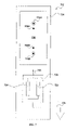
- FIG. 1 illustrates a prior art inductively-coupled plasma processing chamber to facilitate discussion.
- FIG. 2 is a graph of the optical emission of the plasma during an exemplary etch process in which arcing is observed
- FIG. 3 shows a photograph of the interior surface of a silicon carbide plasma-facing component damaged by arcing
- FIGS. 4A and 4B illustrate the function of the resistance circuitry in eliminating arcing.
- FIG. 5 shows, in accordance with one embodiment of the present invention, a circuit diagram for an arc-eliminating (AE) arrangement that also inhibits RF radiation.
- AE arc-eliminating
- FIG. 6 shows, in accordance with one aspect of the present invention, an AE arrangement for a cylindrical chamber wall of an inductively coupled plasma processing chamber
- FIG. 7 shows, in accordance with one embodiment of the present invention, the details of a wall-contacting module.
- FIG. 8 shows, in accordance with an embodiment of the invention, a resistance circuit comprising a plurality of resistors and a switching arrangement.
- the invention relates, in one embodiment, to an arc-eliminating (AE) arrangement for eliminating arcing between a plasma-facing component and the plasma in a plasma processing chamber.
- AE arc-eliminating
- the low resistivity SiC of the chamber wall i.e., the plasma-facing component that experiences arcing later in this example
- the plasma-facing component that experiences arcing later in this example
- the polymer deposition builds up gradually during the period marked by reference number 204 .
- this polymer layer gradually cuts off the conduction path between the plasma through the low resistivity SiC material to ground.
- a DC potential difference builds up across the deposited polymer layer, and the DC potential difference increases as the layer grows thicker over time.
- the DC potential across the deposited polymer layer becomes sufficiently high for arcing to occur across the deposited polymer layer.
- the arc essentially blasts its way through the deposited polymer layer and damages the underlying SiC chamber wall inner surface.
- Anodized aluminum has a higher degree of hardness and is more chemically inert than the bulk aluminum material.
- the anodized aluminum coating that faces the plasma is more insulative.
- the anodized aluminum coating performs the same function as the deposited polymer layer in the example of FIG. 2 , i.e., the insulative anodized aluminum coating restricts the current path from the plasma through the bulk aluminum material of the chamber wall to ground.
- the DC potential difference across the anodized aluminum coating causes arcing to occur.
- the composition of the plasma-facing component such as the chamber wall
- the choice of materials for the plasma-facing component is dictated by considerations other than the electrical properties of the materials. For example, a certain material may be very desirable based on cost considerations, and/or based on the fact that its use causes very little contamination to occur inside the plasma processing chamber, and/or because that material has a superior resistant to the process chemistry, and/or because that material has superior mechanical properties. If one can solve the arcing problem by modifying the electrical properties of the plasma-facing component without requiring the use of a different material, it is possible to increase the variety of materials that can be employed to fabricate the plasma-facing component. This opens up a whole class of materials for use in fabricating plasma-facing components whereas these materials may have been rejected in the past for their poor electrical properties with respect to arcing.
- an appropriately constructed AE circuit is then employed to artificially raise the DC voltage of the plasma-facing component above the ground potential during processing.
- an appropriately-sized resistance circuitry would accomplish the requisite task of eliminating arcing once the plasma-facing component is electrically isolated from ground.
- the resistance circuitry should be carefully selected to elevate the DC voltage of the plasma-facing component to the point where the DC potential difference between the plasma and the plasma-facing component across a dielectric region (such as the aforementioned deposited polymer layer or anodized aluminum coating) is insufficient to cause arcing,
- FIGS. 4A and 4B illustrate the function of the resistance circuitry in eliminating arcing.
- the chamber wall 400 (representing the plasma-facing component in this example) is directly coupled to ground, the entire DC potential difference between the plasma 402 and ground will be concentrated across the dielectric region 404 . It is believed that this DC potential difference, denoted by VA in FIG. 4A , will cause arcing under certain conditions (e.g., once the deposited polymer layer thickens sufficiently or under certain RF voltage and RF power regimes).
- the chamber wall is electrically isolated from ground, and an appropriately-sized resistor R 1 is deliberately inserted in the current path between the plasma-facing component and ground.
- the presence of the resistance circuitry R 1 causes the DC potential difference VA of FIG. 1 to be distributed between VR 1 and VB in this case, wherein VR 1 represents the DC voltage drop across resistor R 1 and VB represents the DC voltage difference between the plasma and the plasma-facing component across dielectric region 404 .
- an RF filter for providing a low impedance path to ground for RF signals to minimize RF radiation at certain frequencies.
- a capacitance circuit is employed as the RF filter.
- the RF filter may be designed to act substantially like an open circuit to the DC signal, thus continuing to allow the DC voltage of the plasma-facing component to be kept off the ground potential (through the use of the resistance circuit).
- the RF filter may be designed to act substantially like a closed circuit, thereby providing a low impedance path to ground for RF signals.
- the RF filter is implemented by an appropriately sized capacitor connected so as to provide an independent low impedance path to ground for the RF signal(s) of interest.
- the RF blocking characteristics of the RF filter may be tuned by using an additional inductor to create an LC bandpass filter.
- Other RF filter designs using active and/or passive components may also be employed.
- Such RF filters, with and without the use of an inductor, are well-known to those skilled in the art.
- FIG. 5 shows, in accordance with one embodiment of the present invention, a circuit diagram for an arc-eliminating (AE) arrangement that also inhibits RF radiation.
- AE arrangement 502 includes an appropriately sized resistance circuit 504 coupled in parallel with an appropriately sized RF filter circuit 506 .
- AE arrangement 502 is interposed in the current path between a plasma-facing component 508 and the ground terminal 510 , with the plasma-facing component 508 otherwise electrically isolated from ground terminal 510 , both the arcing and the radiation of the RF energy is substantially eliminated.
- the value of the resistance circuit should be as high as possible so as to maximize the voltage drop across that resistance circuit (e.g., VR 1 of FIG. 4B ) and therefore minimize the DC potential difference between the plasma and the plasma-facing component (e.g., VB of FIG. 4B ).
- the DC potential difference between the plasma and the plasma-facing component that is primarily responsible for the arcing phenomenon.
- an excessively high value of R 1 will cause VR 1 to be unduly high, which means that the DC potential of the plasma-facing component will be high during and even after processing.
- a very high DC potential on a given component in the chamber represents a potential electrocution hazard.
- the high DC potential is also seen across the RF filter circuit, which may employ some type of capacitance circuit in its design. If the capacitance is charged up to a high voltage and not discharged, or is given insufficient time to discharge, the possibility of electrocution may exist.
- the value of R 1 should be chosen so as to minimize the DC potential difference between the plasma and the plasma-facing component during processing but not to the point where an unnecessary high voltage potential exists on the plasma-facing component and/or across the capacitance circuit of the RF filter and becomes a hazard to the human operator or other devices in the tool environment.
- the resistance circuit may simply be an appropriately sized resistor, e.g., a ceramic resistor.
- the resistance circuit may be constructed out of devices other than a simple passive resistor.
- a range of resistors may be provided, and a switching mechanism or arrangement may be provided to facilitate switching among different resistor values to change the potential difference to vary the non-arcing window for a given process or for different steps of a given process.
- An example of such a design is shown in FIG. 8 .
- a variable resistor may be employed instead.
- a transistor may be employed to implement a variable resistance circuit to raise the DC voltage of the plasma-facing component by a requisite amount (e.g., by varying the gate voltage of the transistor which affects the conductive channel between the source and the drain).
- a requisite amount e.g., by varying the gate voltage of the transistor which affects the conductive channel between the source and the drain.
- any circuit design that provides the requisite resistance value may also be employed.
- the RF filter circuit may simply be an appropriately sized capacitor.
- the value of the capacitor should be sufficiently large such that the RF voltage on the plasma-facing component can be kept relatively low, preferably below the level where RF radiation would interfere with other devices in the processing tool environment.
- the RF filter circuit may be constructed out of devices other than a simple capacitor.
- a tunable RF filter circuit may be employed instead.
- any circuit design that provides the requisite RF filter characteristics may be employed.
- the spatial distribution of the low RF impedance circuits and the high DC resistance circuits are also important for certain plasma-facing components.
- the plasma-facing component is relatively small (e.g., a gas injector nozzle, a probe, and the like)
- a single two-terminal AE arrangement may be employed, with one of its terminals connected to a location on the plasma-facing component and the other terminal connected to ground.
- multiple RF filters may be provided to eliminate RF “hot spots” on the plasma-facing component.
- Multiple RF filters are also advantageous in that they allow the requisite capacitance value to be divided among many parallely connected RF filters, thereby lowering the capacitance value associated with an individual RF filter.
- Multiple parallelly connected RF filters may also be better at handling a large RF current, which is advantageous from a cost and reliability standpoint.
- At a lower capacitance value there may be more choices among the commercially available capacitors and/or the aggregate cost for the multiple capacitors may be lower than the cost of a single high performance capacitor.
- FIG. 6 shows an AE arrangement 600 for a cylindrical chamber wall 602 of an inductively coupled plasma processing chamber.
- chamber wall 602 is electrically isolated from the ground terminal except through AE arrangement 600 .
- AE arrangement 600 includes multiple wall-contacting modules 604 spatially distributed around the chamber wall circumference.
- Each wall-contacting module 604 is preferably made out of a conductive material such as aluminum and is shaped to distribute the electrical contact surface for the DC voltage and the RF signal along the vertical (z) axis of the chamber wall 602 .
- An exemplary individual wall-contacting modules 604 is discussed in greater detail in FIG. 7 hereinbelow.
- each of the wall-contacting modules 604 is provided with a RF filter circuit, which is in the form of a capacitor in the implementation of FIG. 6 .
- a RF filter circuit which is in the form of a capacitor in the implementation of FIG. 6 .
- Each wall-contacting module 604 may also be provided with a resistance circuit to provide a separate path to ground for the DC signal.
- the resistance circuit takes the form of an appropriately sized resistor, for example. However, it is found that for a low resistivity SiC chamber wall, there is no need to distribute the resistors around the circumference of chamber wall 602 in order to eliminate arcing. In one case, a single appropriately sized resistor 610 provided with one of the wall-contacting modules 604 E is sufficient, and other wall-contacting modules may not require the use of a resistance circuit.
- each of the sixteen capacitors on the sixteen wall-contacting modules has a capacitance value that is 390 pF each for a total of 6.24 nF.
- the total capacitance value may be between about 0 pF (i.e., no capacitor) and about 100 nF, more preferably between about 10 pF and about 30 nF and even more preferably between about 1 nF and about 10 nF.
- the total capacitance value may vary depending on, for example, the chamber design, the process parameters and the size of the plasma-facing component being protected. For example, a smaller plasma-facing component may require a smaller capacitor than that required by a larger plasma-facing component. If no capacitance is employed, it is contemplated that an alternative method may be implemented to contain the RF, for example by providing a Faraday shield around the component and/or the chamber that radiates the RF.
- the single resistor in the exemplary implementation has a value of about 500 k ⁇ .
- the resistance value may be between about 1 k ⁇ and about 100 M ⁇ , more preferably between about 10 k ⁇ and about 10 M ⁇ and even more preferably between about 100 k ⁇ and about 1 M ⁇ .
- the resistance value may vary depending on, for example, the chamber design, the process parameters, other electrical characteristics of the plasma-facing component being protected and the like.
- FIG. 7 shows, in accordance with one embodiment of the present invention, the details of a wall-contacting module 702 .
- wall-contacting module 702 both the resistance circuit (in the form of an appropriately sized resistor) and the RF filter circuit (in the form of an appropriately sized capacitor) are present.
- the use of a resistance circuit is not necessary with every wall-contacting module provided at least one of the wall-contacting module is provided with a resistance circuit.
- Wall-contacting module 702 includes a conductive base 704 , which is made out of aluminum or another suitable conductive material.
- the length of conductive base 704 may be adjusted to provide electrical contact along as much of the height of the chamber wall as necessary to avoid RF hot spots.
- the wall-facing side of wall-contacting module 702 may be provided with a RF gasket to further improve RF contact between base 704 and the chamber wall.
- a non-conductive portion 706 made out of, for example, plastic or another suitable non-conductive material is provided and is coupled to base 704 using screws 708 A and 708 B.
- External mounts 710 A and 710 B are then coupled to non-conductive portion 706 .
- External mounts 710 A and 710 B provide the mechanical mounting points to secure the processing chamber, through the wall contacting modules 702 attached thereto, to the frame of the processing system. Since the frame of the processing system is typically grounded, the fact that these external mounts are coupled only to the non-conductive portion of the wall-contacting modules means that the wall-contacting modules and thus the chamber wall are electrically isolated from ground while being securely mounted to the frame of the processing tool.
- An AE arrangement 720 in the form of a PCB board is mounted on base 704 .
- AE arrangement 720 includes a resistor 722 coupled in parallel with a capacitor 724 .
- One end of the RC pair is electrically coupled to base 702 via a conductor 726 .
- the other end of the RC pair is electrically connected to ground via a conductor 728 as shown.
- FIG. 7 shows the application of an AE arrangement to eliminate arcing to the chamber wall
- inventive arc elimination techniques disclosed herein may be applied to eliminate arcing to any other plasma-facing component.
- these plasma-facing components include, without limitation, focus rings, hot edge rings, pressure control devices, chamber liners, probes, gas injector nozzles.
- the inventive arc elimination techniques may also be applied to the substrate to eliminate arcing thereto.
- an appropriate contact arrangement e.g., a spring-loaded pin or multiple pins
- inventive arc elimination techniques disclosed herein are not limited only to inductively coupled plasma processing chambers. It is contemplated that any plasma processing chamber component that experiences arcing may be addressed using the inventive arc elimination techniques irrespective of how the plasma is generated and/or sustained.
- inventive arc elimination techniques disclosed herein may well be employed to reduce arcing to the top electrodes of capacitive etchers.
- plasma elimination techniques disclosed herein may be employed plasma processing systems operating at any RF frequencies.
- inventive arc elimination techniques disclosed herein may be applied to any plasma-facing component irrespective of its composition.
- Applying the inventive AE arrangements to a plasma-facing component that is otherwise electrically isolated from ground modifies its electrical properties as far as susceptibility is arcing is concerned.
- the material of the plasma-facing component may now be selected based on its superior properties in other regards such as chemical inertness, ease of manufacturing, high purity, low cost, desirable mechanical characteristics, ready availability, and the like without regard that material's susceptibility to arcing.
- inventive arc elimination techniques may be applied to plasma-facing components made of materials such as silicon carbide (SiC), silicon (Si), aluminum, stainless steel (i.e., alloys of iron and chromium and optionally nickel, molybdenum, tungsten, copper, silicon, and/or others), and/or other metals and their alloys, boron carbide (B4C), graphite (C), yittrum oxide and other yittria-based materials.
- materials such as silicon carbide (SiC), silicon (Si), aluminum, stainless steel (i.e., alloys of iron and chromium and optionally nickel, molybdenum, tungsten, copper, silicon, and/or others), and/or other metals and their alloys, boron carbide (B4C), graphite (C), yittrum oxide and other yittria-based materials.
- inventive arc elimination techniques may be applied to porous, solid, composite (i.e., multi-layered of the same or different materials), or pure forms of these materials, irrespective of how these materials are deposited, created, or manufactured (such as chemical vapor deposition, plasma-enhanced chemical vapor deposition, sputtered, sintered, plasma-sprayed, pressed, machined, and/or cast).
- inventive arc elimination techniques also apply to material that is made up of multiple layers (e.g., aluminum with an aluminum oxide layer).
Landscapes
- Physics & Mathematics (AREA)
- Engineering & Computer Science (AREA)
- Plasma & Fusion (AREA)
- Chemical & Material Sciences (AREA)
- Analytical Chemistry (AREA)
- Plasma Technology (AREA)
- Drying Of Semiconductors (AREA)
- Physical Vapour Deposition (AREA)
- Chemical Vapour Deposition (AREA)
Abstract
A plasma processing chamber for processing a substrate to form electronic components thereon is disclosed. The plasma processing chamber includes a plasma-facing component having a plasma-facing surface oriented toward a plasma in the plasma processing chamber during processing of the substrate, the plasma-facing component being electrically isolated from a ground terminal. The plasma processing chamber further includes a grounding arrangement coupled to the plasma-facing component, the grounding arrangement including a first resistance circuit disposed in a first current path between the plasma-facing component and the ground terminal. The grounding arrangement further includes a RF filter arrangement disposed in at least one other current path between the plasma-facing component and the ground terminal, wherein a resistance value of the first resistance circuit is selected to substantially eliminate arcing between the plasma and the plasma-facing component during the processing of the substrate.
Description
The present invention relates to apparatus and methods for processing substrates, such as semiconductor substrates for use in IC fabrication or glass panels for use in flat panel display fabrication. More particularly, the present invention relates to improved methods and apparatus for minimizing, during processing, arcing between a plasma-facing component associated with a plasma processing chamber and the plasma present therein and/or with another plasma-facing component.
Plasma processing systems have been around for some time. Over the years, plasma processing systems utilizing inductively coupled plasma sources, electron cyclotron resonance (ECR) sources, capacitive sources, and the like, have been introduced and employed to various degrees to process semiconductor substrates and glass panels.
During processing, multiple deposition and/or etching steps are typically employed. During deposition, materials are deposited onto a substrate surface (such as the surface of a glass panel or a wafer). For example, deposited layers comprising various forms of silicon, silicon dioxide, silicon nitride, metals and the like may be formed on the surface of the substrate. Conversely, etching may be employed to selectively remove materials from predefined areas on the substrate surface. For example, etched features such as vias, contacts, or trenches may be formed in the layers of the substrate. Note that some etch processes may utilize chemistries and/or parameters that simultaneously etch and deposit films on the plasma-facing surfaces.
The plasma can be generated and/or sustained using a variety of plasma generation methods, including inductively-coupled, ECR, microwave and capacitively-coupled plasma methods. In an inductively-coupled plasma processing chamber, for example, an inductive source is employed to generate the plasma. To facilitate discussion, FIG. 1 illustrates a prior art inductive plasma processing chamber 100, which is configured for etching in this example. Plasma processing chamber 100 includes a substantially cylindrical chamber wall portion 102 and an antenna or inductive coil 104 disposed above a dielectric window 106. Typically, antenna 104 is operatively coupled to a first RF power source 108, which may include a RF generator 110 and a RF match network 112 as shown. RF generator 110 may operate at a frequency of, for example 4 MHz. Generally speaking, the RF signals from the RF generators may be sinusoidal, pulsed, or non-sinusoidal. Dielectric window 106 is typically formed of a high resistivity dielectric material, such as high resistivity silicon carbide (SiC).
Within plasma processing chamber 100, a set of inlet gas ports (not shown) is typically provided to facilitate the introduction of gaseous source materials, e.g., the etchant source gases, into the RF-induced plasma region between dielectric window 106 and a substrate 114. Substrate 114 is introduced into chamber 100 and disposed on a chuck 116. Chuck 116 generally acts as an electrode and is operatively coupled to a second RF power source 118, which may include a RF generator 120 and a RF match network 122 as shown. RF generator 120 may operate at a RF frequency of, for example, 13.56 MHz. As mentioned, the RF signal from RF generator 120, like other RF signals from the RF generators, may be sinusoidal, pulsed, or non-sinusoidal.
In order to create a plasma, a process source gas is input into chamber 100 through the aforementioned set of inlet gas ports. Power is then supplied to inductive coil 104 using RF power source 108 and to chuck 116 using RF power source 118. The supplied RF energy from RF power source 108 coupled through dielectric window 106 excites the process source gas and a plasma 124 is generated thereby.
A focus ring 126 may be provided in certain chamber configurations. As is well known to those familiar with the plasma processing art, the focus ring helps focus the ions from plasma 124 onto the surface of substrate 114 to, for example, improve process uniformity. Focus ring 126 also protects a portion of chuck 116 from damage during processing. A plasma screen 128 may also be provided in certain chamber configurations to help contain the plasma and to prevent plasma leakage into non-active areas of the chamber, such as areas below chuck 116. Such leakage may cause premature corrosion and/or result in the inappropriate deposition of unwanted materials on certain chamber parts.
A plurality of magnets 130 may be disposed around the circumference of chamber wall 102. These magnets may be employed, for example, to facilitate control of etch rate uniformity. Chamber 100 may also be provided with different components, depending on the specific manufacturer thereof and/or the requirements of a particular etch process. For example, pressure control rings, hot edge rings, various gas injector nozzles, probes, chamber liners, etc., may also be provided. To simplify the illustration, these well-known components are omitted from FIG. 1 .
Generally speaking, it is critical to maintain tight control of the etch process in order to obtain a satisfactory etch result. Thus, parameters such as the RF voltage, RF power, bias voltage, bias power, plasma density, the amount of contamination in the chamber, and the like, must be carefully controlled. In this regard, the design of the plasma processing chamber, and in particular the design of the plasma-facing components, is tremendously important. As the term is employed herein, a plasma-facing component represents a component that has at least one surface exposed to or facing the plasma during processing. In general, the plasma-facing components in the chamber must be carefully selected in order to obtain the desired combination of reasonable cost, appropriate mechanical strength, compatibility with the etch chemistry, low contamination, appropriate electrical properties, and others.
For example, aluminum, anodized aluminum, or one of the aluminum alloys has long been employed to fabricate plasma-facing components. Although aluminum is relatively inexpensive and easy to fabricate, it suffers from chemical incompatibility with certain etch processes, such as those involved in etching aluminum layers on the substrate surface. Even with an anodized coating or some other coatings, the risk of contamination due to the unwanted presence of aluminum-containing particles in the chamber makes aluminum unacceptable in certain applications. Such aluminum-containing particles may cause unwanted deposition of contaminants on the substrate being processed, or may be incorporated into the polymer deposition along the chamber sidewalls, rendering the chamber cleaning task more difficult and more time-consuming to perform.
Other materials such as silicon carbide (SiC) possess different chemical characteristics, and may thus be employed to fabricate plasma-facing components although the use of SiC may involve trade-offs in cost, electrical properties, and/or mechanical properties. Some materials may have the right chemical and electrical properties but may, for example, be very difficult and/or expensive to fabricate and/or to produce with the requisite degree of purity. Thus, no material is perfect for every application, and one that is chemically compatible and results in low contamination often suffers from other deficiencies, such as undesirable electrical properties. Accordingly, manufacturers constantly try to balance various factors in selecting the “right” material for these plasma-facing components for use in different processing applications
It is observed by the inventors herein that at certain RF power settings in certain processes, arcing may occur between the plasma, such as plasma 124 of FIG. 1 , and a plasma-facing surface of a plasma-facing component. Arcing appears to occur irrespective of whether the plasma-facing surface is in direct contact with the observable plasma cloud of plasma 124. In some cases, if the plasma-facing component is formed of a material having a relatively low resistivity, arcing appears to be more pronounced during certain phases of the process. These low resistivity materials may include, for example, aluminum, stainless steel, various alloys of aluminum and/or stainless steel, low resistivity silicon carbide (SiC), silicon (Si), boron carbide (B4C), graphite (C), and the like. Low resistivity materials are sometimes favored in the fabrication of certain plasma-facing components, such as the chamber wall, because the low resistivity materials appear to be more efficient at containing the RF energy within the chamber. It is also observed that in certain etch processes that cause polymer deposition on a plasma-facing surface, arcing seems to be more pronounced during certain phases of the process.
Arcing is a serious problem, as it detrimentally degrades the process result. For example, FIG. 2 is a graph of the 431 nm optical emission of the plasma during an exemplary etch process in which arcing is observed. As indicated by the transient spikes 202A and 202B in the optical emission signal, the plasma behaves unpredictably during arcing, thus yielding in an unacceptable etch result. Furthermore, the arcing sometimes sputters particles from the plasma-facing surface into the chamber interior, resulting in unwanted contamination at unpredictable times. Still further, arcing causes damage, often serious damage, either immediately or over time to the plasma-facing surface of the plasma-facing component.
For example, FIG. 3 shows a photograph of the interior surface of a silicon carbide plasma-facing component damaged by arcing. In this case, the pattern of the arc tracks 302 is influenced by the magnetic fields associated with the radially disposed magnets that surround the exterior circumference of the chamber wall. It should be pointed out that the magnets happen to be part of the chamber within which the photograph of FIG. 3 was taken; however, the presence or absence of magnets appears not to be a determinant as to whether arcing would occur. The SiC particles displaced from the chamber wall along the arc tracks are introduced into the chamber interior as contaminants. The pitting caused by arc tracks 302 on the chamber wall interior necessitates chamber wall replacement, which is an expensive and time-consuming process and an unwanted interruption in the utilization of the plasma processing chamber in the production of semiconductor products.
Of course, one obvious approach to control arcing would be to simply ground the plasma-facing component, by connecting the plasma-facing component directly to ground. Despite many attempts, directly connecting the plasma-facing component to ground does not always solve the problem. Another approach to control arcing would be to modify other process parameters, such as the RF voltages and RF powers of the various RF power sources. However, this is not always possible since many processes require that certain parameters be kept within a certain range. Still another approach to control arcing would be to select a material having different electrical properties for the plasma-facing components. However, this is also not always a desirable solution since a different material may introduce a different set of problems, such as incompatible chemical properties, increased contamination, increased cost of fabrication, low mechanical strength, and the like.
In view of the foregoing, there are desired improved methods and apparatus for reducing and/or eliminating arcing between a plasma-facing component associated with a plasma processing chamber and the plasma present during processing. Preferably, the techniques for reducing and/or eliminating arcing would be adaptable to any type of material that may be employed to fabricate the plasma-facing components.
The invention relates, in one embodiment, to a plasma processing chamber for processing a substrate to form electronic components thereon. The plasma processing chamber includes a plasma-facing component having a plasma-facing surface oriented toward a plasma in the plasma processing chamber during processing of the substrate, the plasma-facing component being electrically isolated from a ground terminal. The plasma processing chamber further includes a grounding arrangement coupled to the plasma-facing component, the grounding arrangement including a first resistance circuit disposed in a first current path between the plasma-facing component and the ground terminal. The grounding arrangement further includes a RF filter arrangement disposed in at least one other current path between the plasma-facing component and the ground terminal, wherein a resistance value of the first resistance circuit is selected to substantially eliminate arcing between the plasma and the plasma-facing component during the processing of the substrate.
In another embodiment, the invention relates to a method for configuring a plasma processing chamber for processing a substrate to form electronic components thereon. The method includes providing a plasma-facing component having a plasma-facing surface oriented toward a plasma in the plasma processing chamber during the processing of the substrate. The method further includes electrically isolating the plasma-facing component from a ground terminal. The method additionally includes coupling the plasma-facing component to a grounding arrangement, the grounding arrangement comprising a first resistance circuit disposed in a first current path between the plasma-facing component and the ground terminal.
In yet another embodiment, the invention includes a grounding arrangement configured to substantially eliminate arcing between a plasma-facing component associated with a plasma processing chamber and a plasma within the plasma processing chamber. The plasma is present during processing of a substrate to form electronic components thereon. The plasma-facing component has a plasma-facing surface that is oriented toward the plasma during the processing. The plasma-facing component is electrically isolated from a ground terminal. The grounding arrangement includes a resistance circuit configured to be disposed in a first current path between the plasma-facing component and the ground terminal when the grounding arrangement is coupled to the plasma-facing component and the ground terminal, wherein a resistance value of the resistance circuit is selected to substantially eliminate arcing between the plasma and the plasma-facing component during the processing of the substrate.
In yet another embodiment, the invention relates to a method for configuring a plasma processing chamber for processing a substrate to form electronic components thereon. The method includes electrically isolating the substrate from a ground terminal during the processing. The method further includes coupling the substrate to a grounding arrangement during the processing. The grounding arrangement includes a first resistance circuit disposed in a first current path between the substrate and a ground terminal.
These and other features of the present invention will be described in more detail below in the detailed description of the invention and in conjunction with the following figures.
The present invention is illustrated by way of example, and not by way of limitation, in the figures of the accompanying drawings and in which like reference numerals refer to similar elements and in which:
The present invention will now be described in detail with reference to a few preferred embodiments thereof as illustrated in the accompanying drawings. In the following description, numerous specific details are set forth in order to provide a thorough understanding of the present invention. It will be apparent, however, to one skilled in the art, that the present invention may be practiced without some or all of these specific details. In other instances, well known process steps and/or structures have not been described in detail in order to not unnecessarily obscure the present invention.
The invention relates, in one embodiment, to an arc-eliminating (AE) arrangement for eliminating arcing between a plasma-facing component and the plasma in a plasma processing chamber. While not wishing to be bound by theory, it is believed that arcing occurs because a sufficiently high DC potential is allowed to build up across a dielectric layer, such as the polymer layer deposited during processing. This theory is supported, in part, by the behavior of the observed optical emission of the plasma in FIG. 2 . With reference to FIG. 2 , for example, during the period referenced by reference number 204, there is no arcing and the optical emission is stable. The transient spikes 202A and 202B in the optical emission signal represent arcing, which occurs some time after the process has been underway. It is believed that at the beginning of the etch process of FIG. 2 , the low resistivity SiC of the chamber wall (i.e., the plasma-facing component that experiences arcing later in this example) provides a current path to ground for the plasma DC voltage. Thus no arcing occurs at the beginning of the period marked by reference number 204.
As the processing continues, the polymer deposition builds up gradually during the period marked by reference number 204. As the polymer layer is built up along the sidewall, this polymer layer gradually cuts off the conduction path between the plasma through the low resistivity SiC material to ground. Thus, a DC potential difference builds up across the deposited polymer layer, and the DC potential difference increases as the layer grows thicker over time. At some point, the DC potential across the deposited polymer layer becomes sufficiently high for arcing to occur across the deposited polymer layer. At that point, the arc essentially blasts its way through the deposited polymer layer and damages the underlying SiC chamber wall inner surface.
The inventors also realized that this theory may also help explain why arcing sometimes occurs for certain processes at certain RF voltage and power regimes in a chamber that employs an anodized aluminum chamber. Anodized aluminum has a higher degree of hardness and is more chemically inert than the bulk aluminum material. However, while the bulk aluminum material of the chamber wall is highly conductive, the anodized aluminum coating that faces the plasma is more insulative. In one sense, the anodized aluminum coating performs the same function as the deposited polymer layer in the example of FIG. 2 , i.e., the insulative anodized aluminum coating restricts the current path from the plasma through the bulk aluminum material of the chamber wall to ground. Thus, at certain RF voltage and power regimes, the DC potential difference across the anodized aluminum coating causes arcing to occur.
It is further realized that for certain processes, it is impractical to vary process parameters such as the RF voltages and the RF power settings (for the upper and/or lower RF power sources) beyond a certain process window. That is, certain etch or deposition processes can only be successfully performed if the RF voltages and the RF power settings are kept within a given window. Thus, varying the RF voltages and power settings beyond the permissible window in order to eliminate arcing may not be an option in some processes. What is required, thus, is a different way to address the arcing problem.
Furthermore, it is also not always advantageous to change the composition of the plasma-facing component, such as the chamber wall, solely in order to control arcing. This is because many times, the choice of materials for the plasma-facing component is dictated by considerations other than the electrical properties of the materials. For example, a certain material may be very desirable based on cost considerations, and/or based on the fact that its use causes very little contamination to occur inside the plasma processing chamber, and/or because that material has a superior resistant to the process chemistry, and/or because that material has superior mechanical properties. If one can solve the arcing problem by modifying the electrical properties of the plasma-facing component without requiring the use of a different material, it is possible to increase the variety of materials that can be employed to fabricate the plasma-facing component. This opens up a whole class of materials for use in fabricating plasma-facing components whereas these materials may have been rejected in the past for their poor electrical properties with respect to arcing.
Returning to the theory of arcing, it is realized then that simply grounding the plasma-facing component, i.e., directly connecting the plasma-facing component to ground using a conductor, will not reduce the DC potential difference across the deposited polymer layer and/or any dielectric layer and/or dielectric region between the plasma and the plasma-facing component. What is required then is a technique that artificially raises the DC potential of the plasma-facing component so that when the polymer deposition occurs or if the process is executed at certain RF voltages and RF power settings, the DC voltage difference between the plasma and the plasma-facing component is never allowed to reach the point where arcing would occur.
In order to achieve the foregoing, it is important to electrically isolate the plasma-facing component from the ground potential. In real-world terms, since a plasma-facing component, such as the chamber wall, is typically attached to the grounded frame of the plasma processing tool using conductive metal fasteners (e.g., stainless steel screws, bolts, clips, and the like), it is important to devise ways to fasten such plasma-facing component to the grounded frame of the plasma processing tool such that a direct electrical short to ground does not exist. One skilled in the art will readily appreciate that there are myriads of ways to mechanically fasten parts together while keeping them electrically isolated from one another. One such fastening method is discussed later herein in connection with FIG. 7 herein.
Once the plasma-facing component is electrically isolated from ground, an appropriately constructed AE circuit is then employed to artificially raise the DC voltage of the plasma-facing component above the ground potential during processing. For example, an appropriately-sized resistance circuitry would accomplish the requisite task of eliminating arcing once the plasma-facing component is electrically isolated from ground. The resistance circuitry should be carefully selected to elevate the DC voltage of the plasma-facing component to the point where the DC potential difference between the plasma and the plasma-facing component across a dielectric region (such as the aforementioned deposited polymer layer or anodized aluminum coating) is insufficient to cause arcing,
In the situation of FIG. 4B , the chamber wall is electrically isolated from ground, and an appropriately-sized resistor R1 is deliberately inserted in the current path between the plasma-facing component and ground. The presence of the resistance circuitry R1 causes the DC potential difference VA of FIG. 1 to be distributed between VR1 and VB in this case, wherein VR1 represents the DC voltage drop across resistor R1 and VB represents the DC voltage difference between the plasma and the plasma-facing component across dielectric region 404. By choosing an appropriate resistance value for R1 such that VR1 is sufficiently large and thus VB becomes sufficiently small under conditions that may otherwise cause arcing, arcing can be prevented.
Electrically isolating the plasma-facing component from ground and deliberately introducing a resistance circuit into the DC current path between the plasma-facing component and ground appears to substantially reduce the tendency to arc. However, the electrical isolation of the plasma-facing component and the introduction of a resistance circuit into the DC current path may cause other problems under certain conditions. For example, it is known that one must keep the level of radio frequency (RF) radiation output by the plasma-facing component to an acceptable level at all times. Containing the RF energy is important since a high level of RF radiation may cause an undue amount of interference with other electronic devices and may be prohibited by regulations.
If the plasma-facing component were directly connected to ground, as in the case of FIG. 4A , a low impedance path for the RF signal is already provided by the grounding conductor, and one needs to do nothing. However, since a relatively high impedance resistance circuit is required to raise the ground-isolated plasma-facing component closer to the plasma voltage, as in the example of FIG. 4B , an alternative low impedance RF path must be provided if RF containment is required.
In accordance with another aspect of the present invention, there is provided an RF filter for providing a low impedance path to ground for RF signals to minimize RF radiation at certain frequencies. In the preferred embodiment, a capacitance circuit is employed as the RF filter. The RF filter may be designed to act substantially like an open circuit to the DC signal, thus continuing to allow the DC voltage of the plasma-facing component to be kept off the ground potential (through the use of the resistance circuit). To an RF signal, however, the RF filter may be designed to act substantially like a closed circuit, thereby providing a low impedance path to ground for RF signals.
In one embodiment, the RF filter is implemented by an appropriately sized capacitor connected so as to provide an independent low impedance path to ground for the RF signal(s) of interest. The RF blocking characteristics of the RF filter may be tuned by using an additional inductor to create an LC bandpass filter. Other RF filter designs using active and/or passive components may also be employed. Such RF filters, with and without the use of an inductor, are well-known to those skilled in the art.
One would assume that the value of the resistance circuit should be as high as possible so as to maximize the voltage drop across that resistance circuit (e.g., VR1 of FIG. 4B ) and therefore minimize the DC potential difference between the plasma and the plasma-facing component (e.g., VB of FIG. 4B ). As mentioned, it is the DC potential difference between the plasma and the plasma-facing component that is primarily responsible for the arcing phenomenon. However, it should be noted that an excessively high value of R1 will cause VR1 to be unduly high, which means that the DC potential of the plasma-facing component will be high during and even after processing. A very high DC potential on a given component in the chamber represents a potential electrocution hazard. Furthermore, the high DC potential is also seen across the RF filter circuit, which may employ some type of capacitance circuit in its design. If the capacitance is charged up to a high voltage and not discharged, or is given insufficient time to discharge, the possibility of electrocution may exist. Thus, the value of R1 should be chosen so as to minimize the DC potential difference between the plasma and the plasma-facing component during processing but not to the point where an unnecessary high voltage potential exists on the plasma-facing component and/or across the capacitance circuit of the RF filter and becomes a hazard to the human operator or other devices in the tool environment.
In its simplest form, the resistance circuit may simply be an appropriately sized resistor, e.g., a ceramic resistor. One should note that the resistance circuit may be constructed out of devices other than a simple passive resistor. For example, a range of resistors may be provided, and a switching mechanism or arrangement may be provided to facilitate switching among different resistor values to change the potential difference to vary the non-arcing window for a given process or for different steps of a given process. An example of such a design is shown in FIG. 8 . For the purpose of tuning the resistance value to account for different chamber designs, different materials for the plasma-facing components, and/or different process parameters, a variable resistor may be employed instead. As another example, it may be possible to employ a transistor to implement a variable resistance circuit to raise the DC voltage of the plasma-facing component by a requisite amount (e.g., by varying the gate voltage of the transistor which affects the conductive channel between the source and the drain). In fact, any circuit design that provides the requisite resistance value may also be employed. These other resistance circuits are known in the art and will not be discussed in details herein.
Likewise, in its simplest form, the RF filter circuit may simply be an appropriately sized capacitor. The value of the capacitor should be sufficiently large such that the RF voltage on the plasma-facing component can be kept relatively low, preferably below the level where RF radiation would interfere with other devices in the processing tool environment. However, there is an upper limit to the capacitance value for any chamber design since an unduly large capacitor would draw an excessively high RF current, possibly destroying the capacitor itself.
One should note that the RF filter circuit may be constructed out of devices other than a simple capacitor. For the purpose of tuning the RF filter to account for different chamber designs and/or different materials for the plasma-facing components, and/or to selectively block out or let pass RF signals having certain RF frequencies, a tunable RF filter circuit may be employed instead. In fact, any circuit design that provides the requisite RF filter characteristics may be employed. These other RF filter circuits, whether they employ passive and/or active components, are known in the art and will not be discussed in details herein.
The spatial distribution of the low RF impedance circuits and the high DC resistance circuits are also important for certain plasma-facing components. If the plasma-facing component is relatively small (e.g., a gas injector nozzle, a probe, and the like), a single two-terminal AE arrangement may be employed, with one of its terminals connected to a location on the plasma-facing component and the other terminal connected to ground. For larger plasma-facing components and/or for plasma-facing components having more complex shapes, multiple RF filters may be provided to eliminate RF “hot spots” on the plasma-facing component. Multiple RF filters are also advantageous in that they allow the requisite capacitance value to be divided among many parallely connected RF filters, thereby lowering the capacitance value associated with an individual RF filter. Multiple parallelly connected RF filters may also be better at handling a large RF current, which is advantageous from a cost and reliability standpoint. At a lower capacitance value, there may be more choices among the commercially available capacitors and/or the aggregate cost for the multiple capacitors may be lower than the cost of a single high performance capacitor.
In accordance with one aspect of the present invention, FIG. 6 shows an AE arrangement 600 for a cylindrical chamber wall 602 of an inductively coupled plasma processing chamber. In the example of FIG. 6 , chamber wall 602 is electrically isolated from the ground terminal except through AE arrangement 600. AE arrangement 600 includes multiple wall-contacting modules 604 spatially distributed around the chamber wall circumference. Each wall-contacting module 604 is preferably made out of a conductive material such as aluminum and is shaped to distribute the electrical contact surface for the DC voltage and the RF signal along the vertical (z) axis of the chamber wall 602. An exemplary individual wall-contacting modules 604 is discussed in greater detail in FIG. 7 hereinbelow.
In a preferred embodiment, each of the wall-contacting modules 604 is provided with a RF filter circuit, which is in the form of a capacitor in the implementation of FIG. 6 . By distributing the wall contacting modules 604 and thus the RF filter circuits along the circumference of chamber wall 602, RF “hot spots” are minimized. Furthermore, the use of multiple capacitors distributed along the circumference of chamber wall 602 allows the use of a smaller capacitance value for each of the capacitors, which reduces cost and improves reliability as mentioned earlier. In one exemplary implementation, 16 wall-contacting modules are provided. However, if RF hot spots are not a problem and fewer capacitors can reliably keep the RF voltage of the plasma-facing component low to the point where RF radiation no longer poses a problem, only a few or even one RF filter circuit may be necessary.
Each wall-contacting module 604 may also be provided with a resistance circuit to provide a separate path to ground for the DC signal. The resistance circuit takes the form of an appropriately sized resistor, for example. However, it is found that for a low resistivity SiC chamber wall, there is no need to distribute the resistors around the circumference of chamber wall 602 in order to eliminate arcing. In one case, a single appropriately sized resistor 610 provided with one of the wall-contacting modules 604E is sufficient, and other wall-contacting modules may not require the use of a resistance circuit.
In one exemplary implementation, each of the sixteen capacitors on the sixteen wall-contacting modules has a capacitance value that is 390 pF each for a total of 6.24 nF. However, this is for an inductively coupled plasma etching chamber having a low resistivity SiC chamber wall, with an upper electrode running at about 4 MHz and a lower electrode running at about 13.56 MHz during processing. For this case, the total capacitance value may be between about 0 pF (i.e., no capacitor) and about 100 nF, more preferably between about 10 pF and about 30 nF and even more preferably between about 1 nF and about 10 nF. Of course the total capacitance value may vary depending on, for example, the chamber design, the process parameters and the size of the plasma-facing component being protected. For example, a smaller plasma-facing component may require a smaller capacitor than that required by a larger plasma-facing component. If no capacitance is employed, it is contemplated that an alternative method may be implemented to contain the RF, for example by providing a Faraday shield around the component and/or the chamber that radiates the RF.
The single resistor in the exemplary implementation has a value of about 500 kΩ. However, the resistance value may be between about 1 kΩ and about 100 MΩ, more preferably between about 10 kΩ and about 10 MΩ and even more preferably between about 100 kΩ and about 1 MΩ. Of course the resistance value may vary depending on, for example, the chamber design, the process parameters, other electrical characteristics of the plasma-facing component being protected and the like.
In FIG. 7 , the side of the wall-contacting module that faces away from the chamber wall exterior is shown. Wall-contacting module 702 includes a conductive base 704, which is made out of aluminum or another suitable conductive material. The length of conductive base 704 may be adjusted to provide electrical contact along as much of the height of the chamber wall as necessary to avoid RF hot spots. The wall-facing side of wall-contacting module 702 may be provided with a RF gasket to further improve RF contact between base 704 and the chamber wall.
A non-conductive portion 706 made out of, for example, plastic or another suitable non-conductive material is provided and is coupled to base 704 using screws 708A and 708B. External mounts 710A and 710B are then coupled to non-conductive portion 706. External mounts 710A and 710B provide the mechanical mounting points to secure the processing chamber, through the wall contacting modules 702 attached thereto, to the frame of the processing system. Since the frame of the processing system is typically grounded, the fact that these external mounts are coupled only to the non-conductive portion of the wall-contacting modules means that the wall-contacting modules and thus the chamber wall are electrically isolated from ground while being securely mounted to the frame of the processing tool.
An AE arrangement 720 in the form of a PCB board is mounted on base 704. AE arrangement 720 includes a resistor 722 coupled in parallel with a capacitor 724. One end of the RC pair is electrically coupled to base 702 via a conductor 726. The other end of the RC pair is electrically connected to ground via a conductor 728 as shown.
Although FIG. 7 shows the application of an AE arrangement to eliminate arcing to the chamber wall, it should be noted that the inventive arc elimination techniques disclosed herein may be applied to eliminate arcing to any other plasma-facing component. Examples of these plasma-facing components include, without limitation, focus rings, hot edge rings, pressure control devices, chamber liners, probes, gas injector nozzles. In one embodiment, the inventive arc elimination techniques may also be applied to the substrate to eliminate arcing thereto. In one exemplary case, an appropriate contact arrangement (e.g., a spring-loaded pin or multiple pins) may be provided to provide the RF and DC current paths to the substrate.
Furthermore, the inventive arc elimination techniques disclosed herein are not limited only to inductively coupled plasma processing chambers. It is contemplated that any plasma processing chamber component that experiences arcing may be addressed using the inventive arc elimination techniques irrespective of how the plasma is generated and/or sustained. For example, the inventive arc elimination techniques disclosed herein may well be employed to reduce arcing to the top electrodes of capacitive etchers. Furthermore, the plasma elimination techniques disclosed herein may be employed plasma processing systems operating at any RF frequencies.
Even for processes that do not experience arcing within a certain process window, the implementation of the inventive arc elimination techniques widen that process window, allowing the process engineers to employ higher RF power and/or RF voltages, which may result in a better process result whereas these higher RF power and/or RF voltage ranges may have been avoided in the past because of the arcing problem.
Still further, the inventive arc elimination techniques disclosed herein may be applied to any plasma-facing component irrespective of its composition. Applying the inventive AE arrangements to a plasma-facing component that is otherwise electrically isolated from ground modifies its electrical properties as far as susceptibility is arcing is concerned. Thus, the material of the plasma-facing component may now be selected based on its superior properties in other regards such as chemical inertness, ease of manufacturing, high purity, low cost, desirable mechanical characteristics, ready availability, and the like without regard that material's susceptibility to arcing.
As such, it is contemplated that the inventive arc elimination techniques may be applied to plasma-facing components made of materials such as silicon carbide (SiC), silicon (Si), aluminum, stainless steel (i.e., alloys of iron and chromium and optionally nickel, molybdenum, tungsten, copper, silicon, and/or others), and/or other metals and their alloys, boron carbide (B4C), graphite (C), yittrum oxide and other yittria-based materials. Further, the inventive arc elimination techniques may be applied to porous, solid, composite (i.e., multi-layered of the same or different materials), or pure forms of these materials, irrespective of how these materials are deposited, created, or manufactured (such as chemical vapor deposition, plasma-enhanced chemical vapor deposition, sputtered, sintered, plasma-sprayed, pressed, machined, and/or cast). For example, the inventive arc elimination techniques also apply to material that is made up of multiple layers (e.g., aluminum with an aluminum oxide layer). Accordingly, one can now chose a material on account of its desirable chemical properties, mechanical properties, and/or other considerations such as low cost, availability, ease of manufacturing and fabrication, and the like without regard to that material's susceptibility to arcing during processing. If arcing happens to be a problem during processing, the inventive arc elimination techniques may then be employed to eliminate such arcing.
Thus, while this invention has been described in terms of several preferred embodiments, there are alterations, permutations, and equivalents which fall within the scope of this invention. It should also be noted that there are many alternative ways of implementing the methods and apparatuses of the present invention. It is therefore intended that the following appended claims be interpreted as including all such alterations, permutations, and equivalents as fall within the true spirit and scope of the present invention.
Claims (31)
1. A plasma processing chamber for processing a substrate to form electronic components thereon, comprising:
a plasma-facing component having a plasma-facing surface oriented toward a plasma in said plasma processing chamber during processing of said substrate, said plasma-facing component representing a cylindrical chamber wall and being electrically isolated from a ground terminal; and
a grounding arrangement coupled to said plasma-facing component, said grounding arrangement including a first resistance circuit and an RF filter arrangement; disposed in a first current path between said plasma-facing component and said ground terminal, said grounding arrangement further including a plurality of RF filter arrangements disposed in a plurality of current paths between said plasma-facing component and said ground terminal, said plurality of RF filter arrangements being arranged so as to improve distribution of capacitive grounding of said plasma-facing component with respect to at least one surface of said plasma-facing component wherein a resistance value of said first resistance circuit is selected to substantially eliminate arcing between said plasma and said plasma-facing component during said processing of said substrate.
2. The plasma processing chamber of claim 1 where in said plasma-facing component is formed from a material that comprises substantially of boron carbide (B4C).
3. The plasma processing chamber of claim 1 wherein said plasma-facing component is formed from a material that comprises substantially of silicon (Si).
4. The plasma processing chamber of claim 1 wherein said plasma-facing component is formed from a material that comprises substantially of graphite (C).
5. The plasma processing chamber of claim 1 wherein said plasma-facing component is formed from a material that comprises a metal.
6. The plasma processing chamber of claim 5 wherein said metal is aluminum.
7. The plasma processing chamber of claim 5 wherein said metal is steel.
8. The plasma processing chamber of claim 1 wherein said plasma-facing component is formed from a material that comprises substantially of silicon carbide (SiC).
9. The plasma processing chamber of claim 1 wherein said plasma-facing component is formed from a material that includes yittrium.
10. The plasma processing chamber of claim 1 wherein said plasma-facing component is formed from multiple layers of material.
11. The plasma processing chamber of claim 1 wherein said plasma-facing component is formed from a material that includes silicon carbide (SiC).
12. The plasma processing chamber of claim 11 wherein said plasma processing chamber is an inductively-coupled plasma processing chamber.
13. The plasma processing chamber of claim 1 wherein said processing said substrate includes etching said substrate using said plasma.
14. The plasma processing chamber of claim 1 wherein said grounding arrangement includes a plurality of resistance circuits having different resistance values and a switching arrangement, said switching arrangement being configured for selecting one of said plurality of resistance circuits for use as said first resistance circuit.
15. A plasma processing chamber for processing a substrate to form electronic components thereon, comprising:
a plasma-facing component having a plasma-facing surface oriented toward a plasma in said plasma processing chamber during processing of said substrate, said plasma-facing component represents a gas injector nozzle; and
a grounding arrangement coupled to said plasma-facing component, said grounding arrangement including a first resistance circuit disposed in a first current path between said plasma-facing component and said ground terminal, said grounding arrangement further including a first RF filter arrangement disposed in parallel to the first resistance circuit, in a first RF current path between said plasma-facing component and said ground terminal, said first RF filter arrangement being arranged so as to improve distribution of capacitive grounding of said plasma-facing component with respect to at least one surface of said plasma-facing component wherein a resistance value of said first resistance circuit is selected to substantially eliminate arcing between said plasma and said plasma-facing component during said processing of said substrate.
16. The plasma processing chamber of claim 15 wherein said plasma-facing component is said focus ring.
17. The plasma processing chamber of claim 15 wherein said plasma-facing component is said hot edge ring.
18. The plasma processing chamber of claim 15 wherein said plasma-facing component is formed from a material that comprises substantially of silicon carbide (SiC).
19. The plasma processing chamber of claim 15 wherein said plasma-facing component is formed from a material that includes silicon carbide (SiC).
20. The plasma processing chamber of claim 15 wherein said plasma processing chamber is an inductively-coupled plasma processing chamber.
21. The plasma processing chamber of claim 15 wherein said processing said substrate includes etching said substrate using said plasma.
22. The plasma processing chamber of claim 15 wherein said grounding arrangement includes a plurality of resistance circuits having different resistance values and a switching arrangement, said switching arrangement being configured for selecting one of said plurality of resistance circuits for use as said first resistance circuit.
23. The plasma processing chamber of claim 15 wherein said grounding arrangement includes a second RF filter arrangement disposed in a second RF current path between said plasma-facing component and said ground terminal, said second RF filter arrangement being arranged so as to improve said distribution of capacitive grounding of said plasma-facing component with respect to said at least one surface of said plasma-facing component.
24. The plasma processing chamber of claim 15 where in said plasma-facing component is formed from a material that comprises substantially of boron carbide (B4C).
25. The plasma processing chamber of claim 15 wherein said plasma-facing component is formed from a material that comprises substantially of silicon (Si).
26. The plasma processing chamber of claim 15 wherein said plasma-facing component is formed from a material that comprises substantially of graphite (C).
27. The plasma processing chamber of claim 15 wherein said plasma-facing component is formed from a material that comprises a metal.
28. The plasma processing chamber of claim 27 wherein said metal is aluminum.
29. The plasma processing chamber of claim 27 wherein said metal is steel.
30. The plasma processing chamber of claim 15 wherein said plasma-facing component is formed from a material that includes yittrium.
31. The plasma processing chamber of claim 15 wherein said plasma-facing component is formed from multiple layers of material.
Priority Applications (9)
| Application Number | Priority Date | Filing Date | Title |
|---|---|---|---|
| US10/140,618 US7086347B2 (en) | 2002-05-06 | 2002-05-06 | Apparatus and methods for minimizing arcing in a plasma processing chamber |
| PCT/US2003/013597 WO2003096765A2 (en) | 2002-05-06 | 2003-05-01 | Apparatus and methods for minimizing arcing in a plasma processing chamber |
| AU2003228799A AU2003228799A1 (en) | 2002-05-06 | 2003-05-01 | Apparatus and methods for minimizing arcing in a plasma processing chamber |
| EP03726570.9A EP1509942B1 (en) | 2002-05-06 | 2003-05-01 | Apparatus and methods for minimizing arcing in a plasma processing chamber |
| KR1020047017743A KR100993161B1 (en) | 2002-05-06 | 2003-05-01 | Apparatus and method for minimizing arcing of plasma processing chambers |
| JP2004504580A JP4597661B2 (en) | 2002-05-06 | 2003-05-01 | Plasma processing chamber |
| CNB03810377XA CN100447935C (en) | 2002-05-06 | 2003-05-01 | Apparatus and method for minimizing arcing within a plasma processing chamber |
| TW092112083A TWI273653B (en) | 2002-05-06 | 2003-05-02 | Apparatus and methods for minimizing arcing in a plasma processing chamber |
| US11/396,124 US7611640B1 (en) | 2002-05-06 | 2006-03-30 | Minimizing arcing in a plasma processing chamber |
Applications Claiming Priority (1)
| Application Number | Priority Date | Filing Date | Title |
|---|---|---|---|
| US10/140,618 US7086347B2 (en) | 2002-05-06 | 2002-05-06 | Apparatus and methods for minimizing arcing in a plasma processing chamber |
Related Child Applications (1)
| Application Number | Title | Priority Date | Filing Date |
|---|---|---|---|
| US11/396,124 Division US7611640B1 (en) | 2002-05-06 | 2006-03-30 | Minimizing arcing in a plasma processing chamber |
Publications (2)
| Publication Number | Publication Date |
|---|---|
| US20030205327A1 US20030205327A1 (en) | 2003-11-06 |
| US7086347B2 true US7086347B2 (en) | 2006-08-08 |
Family
ID=29269690
Family Applications (2)
| Application Number | Title | Priority Date | Filing Date |
|---|---|---|---|
| US10/140,618 Expired - Lifetime US7086347B2 (en) | 2002-05-06 | 2002-05-06 | Apparatus and methods for minimizing arcing in a plasma processing chamber |
| US11/396,124 Expired - Fee Related US7611640B1 (en) | 2002-05-06 | 2006-03-30 | Minimizing arcing in a plasma processing chamber |
Family Applications After (1)
| Application Number | Title | Priority Date | Filing Date |
|---|---|---|---|
| US11/396,124 Expired - Fee Related US7611640B1 (en) | 2002-05-06 | 2006-03-30 | Minimizing arcing in a plasma processing chamber |
Country Status (8)
| Country | Link |
|---|---|
| US (2) | US7086347B2 (en) |
| EP (1) | EP1509942B1 (en) |
| JP (1) | JP4597661B2 (en) |
| KR (1) | KR100993161B1 (en) |
| CN (1) | CN100447935C (en) |
| AU (1) | AU2003228799A1 (en) |
| TW (1) | TWI273653B (en) |
| WO (1) | WO2003096765A2 (en) |
Cited By (305)
| Publication number | Priority date | Publication date | Assignee | Title |
|---|---|---|---|---|
| US20060241879A1 (en) * | 2005-04-22 | 2006-10-26 | Advanced Energy Industries, Inc. | Arc detection and handling in radio frequency power applications |
| US20080180357A1 (en) * | 2007-01-25 | 2008-07-31 | Kawakami Masatoshi | Plasma processing apparatus |
| US20080194169A1 (en) * | 2007-02-08 | 2008-08-14 | Applied Materials, Inc. | Susceptor with insulative inserts |
| US20080203070A1 (en) * | 2007-02-22 | 2008-08-28 | Milan Ilic | Arc recovery without over-voltage for plasma chamber power supplies using a shunt switch |
| WO2009006152A3 (en) * | 2007-06-28 | 2009-03-19 | Lam Res Corp | Method and apparatus for a voltage/current probe test arrangements |
| US20090280581A1 (en) * | 2008-05-12 | 2009-11-12 | Lam Research Corporation | Detection of arcing events in wafer plasma processing through monitoring of trace gas concentrations |
| US8395078B2 (en) | 2008-12-05 | 2013-03-12 | Advanced Energy Industries, Inc | Arc recovery with over-voltage protection for plasma-chamber power supplies |
| US8542471B2 (en) | 2009-02-17 | 2013-09-24 | Solvix Gmbh | Power supply device for plasma processing |
| US8552665B2 (en) | 2010-08-20 | 2013-10-08 | Advanced Energy Industries, Inc. | Proactive arc management of a plasma load |
| US10844484B2 (en) | 2017-09-22 | 2020-11-24 | Asm Ip Holding B.V. | Apparatus for dispensing a vapor phase reactant to a reaction chamber and related methods |
| US10847366B2 (en) | 2018-11-16 | 2020-11-24 | Asm Ip Holding B.V. | Methods for depositing a transition metal chalcogenide film on a substrate by a cyclical deposition process |
| US10844486B2 (en) | 2009-04-06 | 2020-11-24 | Asm Ip Holding B.V. | Semiconductor processing reactor and components thereof |
| US10851456B2 (en) | 2016-04-21 | 2020-12-01 | Asm Ip Holding B.V. | Deposition of metal borides |
| US10858737B2 (en) | 2014-07-28 | 2020-12-08 | Asm Ip Holding B.V. | Showerhead assembly and components thereof |
| US10867788B2 (en) | 2016-12-28 | 2020-12-15 | Asm Ip Holding B.V. | Method of forming a structure on a substrate |
| US10867786B2 (en) | 2018-03-30 | 2020-12-15 | Asm Ip Holding B.V. | Substrate processing method |
| US10883175B2 (en) | 2018-08-09 | 2021-01-05 | Asm Ip Holding B.V. | Vertical furnace for processing substrates and a liner for use therein |
| US10886123B2 (en) | 2017-06-02 | 2021-01-05 | Asm Ip Holding B.V. | Methods for forming low temperature semiconductor layers and related semiconductor device structures |
| US10892156B2 (en) | 2017-05-08 | 2021-01-12 | Asm Ip Holding B.V. | Methods for forming a silicon nitride film on a substrate and related semiconductor device structures |
| US10910262B2 (en) | 2017-11-16 | 2021-02-02 | Asm Ip Holding B.V. | Method of selectively depositing a capping layer structure on a semiconductor device structure |
| US10914004B2 (en) | 2018-06-29 | 2021-02-09 | Asm Ip Holding B.V. | Thin-film deposition method and manufacturing method of semiconductor device |
| US10923344B2 (en) | 2017-10-30 | 2021-02-16 | Asm Ip Holding B.V. | Methods for forming a semiconductor structure and related semiconductor structures |
| US10928731B2 (en) | 2017-09-21 | 2021-02-23 | Asm Ip Holding B.V. | Method of sequential infiltration synthesis treatment of infiltrateable material and structures and devices formed using same |
| US10934619B2 (en) | 2016-11-15 | 2021-03-02 | Asm Ip Holding B.V. | Gas supply unit and substrate processing apparatus including the gas supply unit |
| US10941490B2 (en) | 2014-10-07 | 2021-03-09 | Asm Ip Holding B.V. | Multiple temperature range susceptor, assembly, reactor and system including the susceptor, and methods of using the same |
| US10943771B2 (en) | 2016-10-26 | 2021-03-09 | Asm Ip Holding B.V. | Methods for thermally calibrating reaction chambers |
| US10950432B2 (en) | 2017-04-25 | 2021-03-16 | Asm Ip Holding B.V. | Method of depositing thin film and method of manufacturing semiconductor device |
| USD913980S1 (en) | 2018-02-01 | 2021-03-23 | Asm Ip Holding B.V. | Gas supply plate for semiconductor manufacturing apparatus |
| US10975470B2 (en) | 2018-02-23 | 2021-04-13 | Asm Ip Holding B.V. | Apparatus for detecting or monitoring for a chemical precursor in a high temperature environment |
| US11004977B2 (en) | 2017-07-19 | 2021-05-11 | Asm Ip Holding B.V. | Method for depositing a group IV semiconductor and related semiconductor device structures |
| US11001925B2 (en) | 2016-12-19 | 2021-05-11 | Asm Ip Holding B.V. | Substrate processing apparatus |
| US11015245B2 (en) | 2014-03-19 | 2021-05-25 | Asm Ip Holding B.V. | Gas-phase reactor and system having exhaust plenum and components thereof |
| US11018047B2 (en) | 2018-01-25 | 2021-05-25 | Asm Ip Holding B.V. | Hybrid lift pin |
| US11018002B2 (en) | 2017-07-19 | 2021-05-25 | Asm Ip Holding B.V. | Method for selectively depositing a Group IV semiconductor and related semiconductor device structures |
| US11022879B2 (en) | 2017-11-24 | 2021-06-01 | Asm Ip Holding B.V. | Method of forming an enhanced unexposed photoresist layer |
| US11024523B2 (en) | 2018-09-11 | 2021-06-01 | Asm Ip Holding B.V. | Substrate processing apparatus and method |
| US11031242B2 (en) | 2018-11-07 | 2021-06-08 | Asm Ip Holding B.V. | Methods for depositing a boron doped silicon germanium film |
| USD922229S1 (en) | 2019-06-05 | 2021-06-15 | Asm Ip Holding B.V. | Device for controlling a temperature of a gas supply unit |
| US11049751B2 (en) | 2018-09-14 | 2021-06-29 | Asm Ip Holding B.V. | Cassette supply system to store and handle cassettes and processing apparatus equipped therewith |
| US11056567B2 (en) | 2018-05-11 | 2021-07-06 | Asm Ip Holding B.V. | Method of forming a doped metal carbide film on a substrate and related semiconductor device structures |
| US11053591B2 (en) | 2018-08-06 | 2021-07-06 | Asm Ip Holding B.V. | Multi-port gas injection system and reactor system including same |
| US11056344B2 (en) | 2017-08-30 | 2021-07-06 | Asm Ip Holding B.V. | Layer forming method |
| US11069510B2 (en) | 2017-08-30 | 2021-07-20 | Asm Ip Holding B.V. | Substrate processing apparatus |
| US11081345B2 (en) | 2018-02-06 | 2021-08-03 | Asm Ip Holding B.V. | Method of post-deposition treatment for silicon oxide film |
| US11088002B2 (en) | 2018-03-29 | 2021-08-10 | Asm Ip Holding B.V. | Substrate rack and a substrate processing system and method |
| US11087997B2 (en) | 2018-10-31 | 2021-08-10 | Asm Ip Holding B.V. | Substrate processing apparatus for processing substrates |
| US11094546B2 (en) | 2017-10-05 | 2021-08-17 | Asm Ip Holding B.V. | Method for selectively depositing a metallic film on a substrate |
| US11094582B2 (en) | 2016-07-08 | 2021-08-17 | Asm Ip Holding B.V. | Selective deposition method to form air gaps |
| US11101370B2 (en) | 2016-05-02 | 2021-08-24 | Asm Ip Holding B.V. | Method of forming a germanium oxynitride film |
| US11107676B2 (en) | 2016-07-28 | 2021-08-31 | Asm Ip Holding B.V. | Method and apparatus for filling a gap |
| US11114294B2 (en) | 2019-03-08 | 2021-09-07 | Asm Ip Holding B.V. | Structure including SiOC layer and method of forming same |
| US11114283B2 (en) * | 2018-03-16 | 2021-09-07 | Asm Ip Holding B.V. | Reactor, system including the reactor, and methods of manufacturing and using same |
| USD930782S1 (en) | 2019-08-22 | 2021-09-14 | Asm Ip Holding B.V. | Gas distributor |
| US11127589B2 (en) | 2019-02-01 | 2021-09-21 | Asm Ip Holding B.V. | Method of topology-selective film formation of silicon oxide |
| US11127617B2 (en) | 2017-11-27 | 2021-09-21 | Asm Ip Holding B.V. | Storage device for storing wafer cassettes for use with a batch furnace |
| USD931978S1 (en) | 2019-06-27 | 2021-09-28 | Asm Ip Holding B.V. | Showerhead vacuum transport |
| US11139191B2 (en) | 2017-08-09 | 2021-10-05 | Asm Ip Holding B.V. | Storage apparatus for storing cassettes for substrates and processing apparatus equipped therewith |
| US11139308B2 (en) | 2015-12-29 | 2021-10-05 | Asm Ip Holding B.V. | Atomic layer deposition of III-V compounds to form V-NAND devices |
| US11158513B2 (en) | 2018-12-13 | 2021-10-26 | Asm Ip Holding B.V. | Methods for forming a rhenium-containing film on a substrate by a cyclical deposition process and related semiconductor device structures |
| US11164955B2 (en) | 2017-07-18 | 2021-11-02 | Asm Ip Holding B.V. | Methods for forming a semiconductor device structure and related semiconductor device structures |
| US11168395B2 (en) | 2018-06-29 | 2021-11-09 | Asm Ip Holding B.V. | Temperature-controlled flange and reactor system including same |
| US11171025B2 (en) | 2019-01-22 | 2021-11-09 | Asm Ip Holding B.V. | Substrate processing device |
| USD935572S1 (en) | 2019-05-24 | 2021-11-09 | Asm Ip Holding B.V. | Gas channel plate |
| US11205585B2 (en) | 2016-07-28 | 2021-12-21 | Asm Ip Holding B.V. | Substrate processing apparatus and method of operating the same |
| US11217444B2 (en) | 2018-11-30 | 2022-01-04 | Asm Ip Holding B.V. | Method for forming an ultraviolet radiation responsive metal oxide-containing film |
| US11222772B2 (en) | 2016-12-14 | 2022-01-11 | Asm Ip Holding B.V. | Substrate processing apparatus |
| USD940837S1 (en) | 2019-08-22 | 2022-01-11 | Asm Ip Holding B.V. | Electrode |
| US11227789B2 (en) | 2019-02-20 | 2022-01-18 | Asm Ip Holding B.V. | Method and apparatus for filling a recess formed within a substrate surface |
| US11227782B2 (en) | 2019-07-31 | 2022-01-18 | Asm Ip Holding B.V. | Vertical batch furnace assembly |
| US11232963B2 (en) | 2018-10-03 | 2022-01-25 | Asm Ip Holding B.V. | Substrate processing apparatus and method |
| US11230766B2 (en) | 2018-03-29 | 2022-01-25 | Asm Ip Holding B.V. | Substrate processing apparatus and method |
| US11233133B2 (en) | 2015-10-21 | 2022-01-25 | Asm Ip Holding B.V. | NbMC layers |
| US11242598B2 (en) | 2015-06-26 | 2022-02-08 | Asm Ip Holding B.V. | Structures including metal carbide material, devices including the structures, and methods of forming same |
| US11251068B2 (en) | 2018-10-19 | 2022-02-15 | Asm Ip Holding B.V. | Substrate processing apparatus and substrate processing method |
| US11251040B2 (en) | 2019-02-20 | 2022-02-15 | Asm Ip Holding B.V. | Cyclical deposition method including treatment step and apparatus for same |
| US11251035B2 (en) | 2016-12-22 | 2022-02-15 | Asm Ip Holding B.V. | Method of forming a structure on a substrate |
| USD944946S1 (en) | 2019-06-14 | 2022-03-01 | Asm Ip Holding B.V. | Shower plate |
| US11270899B2 (en) | 2018-06-04 | 2022-03-08 | Asm Ip Holding B.V. | Wafer handling chamber with moisture reduction |
| US11274369B2 (en) | 2018-09-11 | 2022-03-15 | Asm Ip Holding B.V. | Thin film deposition method |
| US11282698B2 (en) | 2019-07-19 | 2022-03-22 | Asm Ip Holding B.V. | Method of forming topology-controlled amorphous carbon polymer film |
| US11289326B2 (en) | 2019-05-07 | 2022-03-29 | Asm Ip Holding B.V. | Method for reforming amorphous carbon polymer film |
| US11286562B2 (en) | 2018-06-08 | 2022-03-29 | Asm Ip Holding B.V. | Gas-phase chemical reactor and method of using same |
| US11286558B2 (en) | 2019-08-23 | 2022-03-29 | Asm Ip Holding B.V. | Methods for depositing a molybdenum nitride film on a surface of a substrate by a cyclical deposition process and related semiconductor device structures including a molybdenum nitride film |
| USD947913S1 (en) | 2019-05-17 | 2022-04-05 | Asm Ip Holding B.V. | Susceptor shaft |
| US11295980B2 (en) | 2017-08-30 | 2022-04-05 | Asm Ip Holding B.V. | Methods for depositing a molybdenum metal film over a dielectric surface of a substrate by a cyclical deposition process and related semiconductor device structures |
| US11296189B2 (en) | 2018-06-21 | 2022-04-05 | Asm Ip Holding B.V. | Method for depositing a phosphorus doped silicon arsenide film and related semiconductor device structures |
| USD948463S1 (en) | 2018-10-24 | 2022-04-12 | Asm Ip Holding B.V. | Susceptor for semiconductor substrate supporting apparatus |
| USD949319S1 (en) | 2019-08-22 | 2022-04-19 | Asm Ip Holding B.V. | Exhaust duct |
| US11306395B2 (en) | 2017-06-28 | 2022-04-19 | Asm Ip Holding B.V. | Methods for depositing a transition metal nitride film on a substrate by atomic layer deposition and related deposition apparatus |
| US11315794B2 (en) | 2019-10-21 | 2022-04-26 | Asm Ip Holding B.V. | Apparatus and methods for selectively etching films |
| US11342216B2 (en) | 2019-02-20 | 2022-05-24 | Asm Ip Holding B.V. | Cyclical deposition method and apparatus for filling a recess formed within a substrate surface |
| US11339476B2 (en) | 2019-10-08 | 2022-05-24 | Asm Ip Holding B.V. | Substrate processing device having connection plates, substrate processing method |
| US11345999B2 (en) | 2019-06-06 | 2022-05-31 | Asm Ip Holding B.V. | Method of using a gas-phase reactor system including analyzing exhausted gas |
| US11355338B2 (en) | 2019-05-10 | 2022-06-07 | Asm Ip Holding B.V. | Method of depositing material onto a surface and structure formed according to the method |
| US11361990B2 (en) | 2018-05-28 | 2022-06-14 | Asm Ip Holding B.V. | Substrate processing method and device manufactured by using the same |
| US11374112B2 (en) | 2017-07-19 | 2022-06-28 | Asm Ip Holding B.V. | Method for depositing a group IV semiconductor and related semiconductor device structures |
| US11378337B2 (en) | 2019-03-28 | 2022-07-05 | Asm Ip Holding B.V. | Door opener and substrate processing apparatus provided therewith |
| US11387120B2 (en) | 2017-09-28 | 2022-07-12 | Asm Ip Holding B.V. | Chemical dispensing apparatus and methods for dispensing a chemical to a reaction chamber |
| US11387106B2 (en) | 2018-02-14 | 2022-07-12 | Asm Ip Holding B.V. | Method for depositing a ruthenium-containing film on a substrate by a cyclical deposition process |
| US11390945B2 (en) | 2019-07-03 | 2022-07-19 | Asm Ip Holding B.V. | Temperature control assembly for substrate processing apparatus and method of using same |
| US11393690B2 (en) | 2018-01-19 | 2022-07-19 | Asm Ip Holding B.V. | Deposition method |
| US11390946B2 (en) | 2019-01-17 | 2022-07-19 | Asm Ip Holding B.V. | Methods of forming a transition metal containing film on a substrate by a cyclical deposition process |
| US11390950B2 (en) | 2017-01-10 | 2022-07-19 | Asm Ip Holding B.V. | Reactor system and method to reduce residue buildup during a film deposition process |
| US11398382B2 (en) | 2018-03-27 | 2022-07-26 | Asm Ip Holding B.V. | Method of forming an electrode on a substrate and a semiconductor device structure including an electrode |
| US11401605B2 (en) | 2019-11-26 | 2022-08-02 | Asm Ip Holding B.V. | Substrate processing apparatus |
| US11411088B2 (en) | 2018-11-16 | 2022-08-09 | Asm Ip Holding B.V. | Methods for forming a metal silicate film on a substrate in a reaction chamber and related semiconductor device structures |
| US11410851B2 (en) | 2017-02-15 | 2022-08-09 | Asm Ip Holding B.V. | Methods for forming a metallic film on a substrate by cyclical deposition and related semiconductor device structures |
| US11414760B2 (en) | 2018-10-08 | 2022-08-16 | Asm Ip Holding B.V. | Substrate support unit, thin film deposition apparatus including the same, and substrate processing apparatus including the same |
| US11417545B2 (en) | 2017-08-08 | 2022-08-16 | Asm Ip Holding B.V. | Radiation shield |
| US11424119B2 (en) | 2019-03-08 | 2022-08-23 | Asm Ip Holding B.V. | Method for selective deposition of silicon nitride layer and structure including selectively-deposited silicon nitride layer |
| US11430674B2 (en) | 2018-08-22 | 2022-08-30 | Asm Ip Holding B.V. | Sensor array, apparatus for dispensing a vapor phase reactant to a reaction chamber and related methods |
| US11430640B2 (en) | 2019-07-30 | 2022-08-30 | Asm Ip Holding B.V. | Substrate processing apparatus |
| US11437241B2 (en) | 2020-04-08 | 2022-09-06 | Asm Ip Holding B.V. | Apparatus and methods for selectively etching silicon oxide films |
| US11443926B2 (en) | 2019-07-30 | 2022-09-13 | Asm Ip Holding B.V. | Substrate processing apparatus |
| US11447861B2 (en) | 2016-12-15 | 2022-09-20 | Asm Ip Holding B.V. | Sequential infiltration synthesis apparatus and a method of forming a patterned structure |
| US11447864B2 (en) | 2019-04-19 | 2022-09-20 | Asm Ip Holding B.V. | Layer forming method and apparatus |
| US11453943B2 (en) | 2016-05-25 | 2022-09-27 | Asm Ip Holding B.V. | Method for forming carbon-containing silicon/metal oxide or nitride film by ALD using silicon precursor and hydrocarbon precursor |
| USD965044S1 (en) | 2019-08-19 | 2022-09-27 | Asm Ip Holding B.V. | Susceptor shaft |
| USD965524S1 (en) | 2019-08-19 | 2022-10-04 | Asm Ip Holding B.V. | Susceptor support |
| US11469098B2 (en) | 2018-05-08 | 2022-10-11 | Asm Ip Holding B.V. | Methods for depositing an oxide film on a substrate by a cyclical deposition process and related device structures |
| US11473195B2 (en) | 2018-03-01 | 2022-10-18 | Asm Ip Holding B.V. | Semiconductor processing apparatus and a method for processing a substrate |
| US11476109B2 (en) | 2019-06-11 | 2022-10-18 | Asm Ip Holding B.V. | Method of forming an electronic structure using reforming gas, system for performing the method, and structure formed using the method |
| US11482533B2 (en) | 2019-02-20 | 2022-10-25 | Asm Ip Holding B.V. | Apparatus and methods for plug fill deposition in 3-D NAND applications |
| US11482418B2 (en) | 2018-02-20 | 2022-10-25 | Asm Ip Holding B.V. | Substrate processing method and apparatus |
| US11482412B2 (en) | 2018-01-19 | 2022-10-25 | Asm Ip Holding B.V. | Method for depositing a gap-fill layer by plasma-assisted deposition |
| US11488854B2 (en) | 2020-03-11 | 2022-11-01 | Asm Ip Holding B.V. | Substrate handling device with adjustable joints |
| US11488819B2 (en) | 2018-12-04 | 2022-11-01 | Asm Ip Holding B.V. | Method of cleaning substrate processing apparatus |
| US11495459B2 (en) | 2019-09-04 | 2022-11-08 | Asm Ip Holding B.V. | Methods for selective deposition using a sacrificial capping layer |
| US11492703B2 (en) | 2018-06-27 | 2022-11-08 | Asm Ip Holding B.V. | Cyclic deposition methods for forming metal-containing material and films and structures including the metal-containing material |
| US11499222B2 (en) | 2018-06-27 | 2022-11-15 | Asm Ip Holding B.V. | Cyclic deposition methods for forming metal-containing material and films and structures including the metal-containing material |
| US11501968B2 (en) | 2019-11-15 | 2022-11-15 | Asm Ip Holding B.V. | Method for providing a semiconductor device with silicon filled gaps |
| US11501956B2 (en) | 2012-10-12 | 2022-11-15 | Asm Ip Holding B.V. | Semiconductor reaction chamber showerhead |
| US11499226B2 (en) | 2018-11-02 | 2022-11-15 | Asm Ip Holding B.V. | Substrate supporting unit and a substrate processing device including the same |
| US11501973B2 (en) | 2018-01-16 | 2022-11-15 | Asm Ip Holding B.V. | Method for depositing a material film on a substrate within a reaction chamber by a cyclical deposition process and related device structures |
| US11515188B2 (en) | 2019-05-16 | 2022-11-29 | Asm Ip Holding B.V. | Wafer boat handling device, vertical batch furnace and method |
| US11515187B2 (en) | 2020-05-01 | 2022-11-29 | Asm Ip Holding B.V. | Fast FOUP swapping with a FOUP handler |
| US11521851B2 (en) | 2020-02-03 | 2022-12-06 | Asm Ip Holding B.V. | Method of forming structures including a vanadium or indium layer |
| US11527400B2 (en) | 2019-08-23 | 2022-12-13 | Asm Ip Holding B.V. | Method for depositing silicon oxide film having improved quality by peald using bis(diethylamino)silane |
| US11527403B2 (en) | 2019-12-19 | 2022-12-13 | Asm Ip Holding B.V. | Methods for filling a gap feature on a substrate surface and related semiconductor structures |
| US11530483B2 (en) | 2018-06-21 | 2022-12-20 | Asm Ip Holding B.V. | Substrate processing system |
| US11532757B2 (en) | 2016-10-27 | 2022-12-20 | Asm Ip Holding B.V. | Deposition of charge trapping layers |
| US11530876B2 (en) | 2020-04-24 | 2022-12-20 | Asm Ip Holding B.V. | Vertical batch furnace assembly comprising a cooling gas supply |
| US11551925B2 (en) | 2019-04-01 | 2023-01-10 | Asm Ip Holding B.V. | Method for manufacturing a semiconductor device |
| US11551912B2 (en) | 2020-01-20 | 2023-01-10 | Asm Ip Holding B.V. | Method of forming thin film and method of modifying surface of thin film |
| USD975665S1 (en) | 2019-05-17 | 2023-01-17 | Asm Ip Holding B.V. | Susceptor shaft |
| US11557474B2 (en) | 2019-07-29 | 2023-01-17 | Asm Ip Holding B.V. | Methods for selective deposition utilizing n-type dopants and/or alternative dopants to achieve high dopant incorporation |
| US11562901B2 (en) | 2019-09-25 | 2023-01-24 | Asm Ip Holding B.V. | Substrate processing method |
| US11572620B2 (en) | 2018-11-06 | 2023-02-07 | Asm Ip Holding B.V. | Methods for selectively depositing an amorphous silicon film on a substrate |
| US11581186B2 (en) | 2016-12-15 | 2023-02-14 | Asm Ip Holding B.V. | Sequential infiltration synthesis apparatus |
| US11587815B2 (en) | 2019-07-31 | 2023-02-21 | Asm Ip Holding B.V. | Vertical batch furnace assembly |
| US11587814B2 (en) | 2019-07-31 | 2023-02-21 | Asm Ip Holding B.V. | Vertical batch furnace assembly |
| US11587821B2 (en) | 2017-08-08 | 2023-02-21 | Asm Ip Holding B.V. | Substrate lift mechanism and reactor including same |
| US11594450B2 (en) | 2019-08-22 | 2023-02-28 | Asm Ip Holding B.V. | Method for forming a structure with a hole |
| US11594600B2 (en) | 2019-11-05 | 2023-02-28 | Asm Ip Holding B.V. | Structures with doped semiconductor layers and methods and systems for forming same |
| USD979506S1 (en) | 2019-08-22 | 2023-02-28 | Asm Ip Holding B.V. | Insulator |
| USD980814S1 (en) | 2021-05-11 | 2023-03-14 | Asm Ip Holding B.V. | Gas distributor for substrate processing apparatus |
| US11605528B2 (en) | 2019-07-09 | 2023-03-14 | Asm Ip Holding B.V. | Plasma device using coaxial waveguide, and substrate treatment method |
| USD980813S1 (en) | 2021-05-11 | 2023-03-14 | Asm Ip Holding B.V. | Gas flow control plate for substrate processing apparatus |
| US11610774B2 (en) | 2019-10-02 | 2023-03-21 | Asm Ip Holding B.V. | Methods for forming a topographically selective silicon oxide film by a cyclical plasma-enhanced deposition process |
| US11610775B2 (en) | 2016-07-28 | 2023-03-21 | Asm Ip Holding B.V. | Method and apparatus for filling a gap |
| USD981973S1 (en) | 2021-05-11 | 2023-03-28 | Asm Ip Holding B.V. | Reactor wall for substrate processing apparatus |
| US11615970B2 (en) | 2019-07-17 | 2023-03-28 | Asm Ip Holding B.V. | Radical assist ignition plasma system and method |
| US11626308B2 (en) | 2020-05-13 | 2023-04-11 | Asm Ip Holding B.V. | Laser alignment fixture for a reactor system |
| US11626316B2 (en) | 2019-11-20 | 2023-04-11 | Asm Ip Holding B.V. | Method of depositing carbon-containing material on a surface of a substrate, structure formed using the method, and system for forming the structure |
| US11629407B2 (en) | 2019-02-22 | 2023-04-18 | Asm Ip Holding B.V. | Substrate processing apparatus and method for processing substrates |
| US11629406B2 (en) | 2018-03-09 | 2023-04-18 | Asm Ip Holding B.V. | Semiconductor processing apparatus comprising one or more pyrometers for measuring a temperature of a substrate during transfer of the substrate |
| US11637014B2 (en) | 2019-10-17 | 2023-04-25 | Asm Ip Holding B.V. | Methods for selective deposition of doped semiconductor material |
| US11637011B2 (en) | 2019-10-16 | 2023-04-25 | Asm Ip Holding B.V. | Method of topology-selective film formation of silicon oxide |
| US11639811B2 (en) | 2017-11-27 | 2023-05-02 | Asm Ip Holding B.V. | Apparatus including a clean mini environment |
| US11639548B2 (en) | 2019-08-21 | 2023-05-02 | Asm Ip Holding B.V. | Film-forming material mixed-gas forming device and film forming device |
| US11646204B2 (en) | 2020-06-24 | 2023-05-09 | Asm Ip Holding B.V. | Method for forming a layer provided with silicon |
| US11644758B2 (en) | 2020-07-17 | 2023-05-09 | Asm Ip Holding B.V. | Structures and methods for use in photolithography |
| US11646184B2 (en) | 2019-11-29 | 2023-05-09 | Asm Ip Holding B.V. | Substrate processing apparatus |
| US11646197B2 (en) | 2018-07-03 | 2023-05-09 | Asm Ip Holding B.V. | Method for depositing silicon-free carbon-containing film as gap-fill layer by pulse plasma-assisted deposition |
| US11646205B2 (en) | 2019-10-29 | 2023-05-09 | Asm Ip Holding B.V. | Methods of selectively forming n-type doped material on a surface, systems for selectively forming n-type doped material, and structures formed using same |
| US11643724B2 (en) | 2019-07-18 | 2023-05-09 | Asm Ip Holding B.V. | Method of forming structures using a neutral beam |
| US11649546B2 (en) | 2016-07-08 | 2023-05-16 | Asm Ip Holding B.V. | Organic reactants for atomic layer deposition |
| US11658029B2 (en) | 2018-12-14 | 2023-05-23 | Asm Ip Holding B.V. | Method of forming a device structure using selective deposition of gallium nitride and system for same |
| US11658030B2 (en) | 2017-03-29 | 2023-05-23 | Asm Ip Holding B.V. | Method for forming doped metal oxide films on a substrate by cyclical deposition and related semiconductor device structures |
| US11658035B2 (en) | 2020-06-30 | 2023-05-23 | Asm Ip Holding B.V. | Substrate processing method |
| US11664267B2 (en) | 2019-07-10 | 2023-05-30 | Asm Ip Holding B.V. | Substrate support assembly and substrate processing device including the same |
| US11664245B2 (en) | 2019-07-16 | 2023-05-30 | Asm Ip Holding B.V. | Substrate processing device |
| US11664199B2 (en) | 2018-10-19 | 2023-05-30 | Asm Ip Holding B.V. | Substrate processing apparatus and substrate processing method |
| US11676812B2 (en) | 2016-02-19 | 2023-06-13 | Asm Ip Holding B.V. | Method for forming silicon nitride film selectively on top/bottom portions |
| US11674220B2 (en) | 2020-07-20 | 2023-06-13 | Asm Ip Holding B.V. | Method for depositing molybdenum layers using an underlayer |
| US11680839B2 (en) | 2019-08-05 | 2023-06-20 | Asm Ip Holding B.V. | Liquid level sensor for a chemical source vessel |
| USD990534S1 (en) | 2020-09-11 | 2023-06-27 | Asm Ip Holding B.V. | Weighted lift pin |
| USD990441S1 (en) | 2021-09-07 | 2023-06-27 | Asm Ip Holding B.V. | Gas flow control plate |
| US11685991B2 (en) | 2018-02-14 | 2023-06-27 | Asm Ip Holding B.V. | Method for depositing a ruthenium-containing film on a substrate by a cyclical deposition process |
| US11688603B2 (en) | 2019-07-17 | 2023-06-27 | Asm Ip Holding B.V. | Methods of forming silicon germanium structures |
| US11705333B2 (en) | 2020-05-21 | 2023-07-18 | Asm Ip Holding B.V. | Structures including multiple carbon layers and methods of forming and using same |
| US11718913B2 (en) | 2018-06-04 | 2023-08-08 | Asm Ip Holding B.V. | Gas distribution system and reactor system including same |
| US11725277B2 (en) | 2011-07-20 | 2023-08-15 | Asm Ip Holding B.V. | Pressure transmitter for a semiconductor processing environment |
| US11725280B2 (en) | 2020-08-26 | 2023-08-15 | Asm Ip Holding B.V. | Method for forming metal silicon oxide and metal silicon oxynitride layers |
| US11735422B2 (en) | 2019-10-10 | 2023-08-22 | Asm Ip Holding B.V. | Method of forming a photoresist underlayer and structure including same |
| US11742198B2 (en) | 2019-03-08 | 2023-08-29 | Asm Ip Holding B.V. | Structure including SiOCN layer and method of forming same |
| US11742189B2 (en) | 2015-03-12 | 2023-08-29 | Asm Ip Holding B.V. | Multi-zone reactor, system including the reactor, and method of using the same |
| US11767589B2 (en) | 2020-05-29 | 2023-09-26 | Asm Ip Holding B.V. | Substrate processing device |
| US11769682B2 (en) | 2017-08-09 | 2023-09-26 | Asm Ip Holding B.V. | Storage apparatus for storing cassettes for substrates and processing apparatus equipped therewith |
| US11776846B2 (en) | 2020-02-07 | 2023-10-03 | Asm Ip Holding B.V. | Methods for depositing gap filling fluids and related systems and devices |
| US11781243B2 (en) | 2020-02-17 | 2023-10-10 | Asm Ip Holding B.V. | Method for depositing low temperature phosphorous-doped silicon |
| US11781221B2 (en) | 2019-05-07 | 2023-10-10 | Asm Ip Holding B.V. | Chemical source vessel with dip tube |
| US11802338B2 (en) | 2017-07-26 | 2023-10-31 | Asm Ip Holding B.V. | Chemical treatment, deposition and/or infiltration apparatus and method for using the same |
| US11804364B2 (en) | 2020-05-19 | 2023-10-31 | Asm Ip Holding B.V. | Substrate processing apparatus |
| US11810788B2 (en) | 2016-11-01 | 2023-11-07 | Asm Ip Holding B.V. | Methods for forming a transition metal niobium nitride film on a substrate by atomic layer deposition and related semiconductor device structures |
| US11814747B2 (en) | 2019-04-24 | 2023-11-14 | Asm Ip Holding B.V. | Gas-phase reactor system-with a reaction chamber, a solid precursor source vessel, a gas distribution system, and a flange assembly |
| US11823876B2 (en) | 2019-09-05 | 2023-11-21 | Asm Ip Holding B.V. | Substrate processing apparatus |
| US11821078B2 (en) | 2020-04-15 | 2023-11-21 | Asm Ip Holding B.V. | Method for forming precoat film and method for forming silicon-containing film |
| US11823866B2 (en) | 2020-04-02 | 2023-11-21 | Asm Ip Holding B.V. | Thin film forming method |
| US11830730B2 (en) | 2017-08-29 | 2023-11-28 | Asm Ip Holding B.V. | Layer forming method and apparatus |
| US11828707B2 (en) | 2020-02-04 | 2023-11-28 | Asm Ip Holding B.V. | Method and apparatus for transmittance measurements of large articles |
| US11830738B2 (en) | 2020-04-03 | 2023-11-28 | Asm Ip Holding B.V. | Method for forming barrier layer and method for manufacturing semiconductor device |
| US11827981B2 (en) | 2020-10-14 | 2023-11-28 | Asm Ip Holding B.V. | Method of depositing material on stepped structure |
| US11840761B2 (en) | 2019-12-04 | 2023-12-12 | Asm Ip Holding B.V. | Substrate processing apparatus |
| US11848200B2 (en) | 2017-05-08 | 2023-12-19 | Asm Ip Holding B.V. | Methods for selectively forming a silicon nitride film on a substrate and related semiconductor device structures |
| US11876356B2 (en) | 2020-03-11 | 2024-01-16 | Asm Ip Holding B.V. | Lockout tagout assembly and system and method of using same |
| US11873557B2 (en) | 2020-10-22 | 2024-01-16 | Asm Ip Holding B.V. | Method of depositing vanadium metal |
| USD1012873S1 (en) | 2020-09-24 | 2024-01-30 | Asm Ip Holding B.V. | Electrode for semiconductor processing apparatus |
| US11885020B2 (en) | 2020-12-22 | 2024-01-30 | Asm Ip Holding B.V. | Transition metal deposition method |
| US11887857B2 (en) | 2020-04-24 | 2024-01-30 | Asm Ip Holding B.V. | Methods and systems for depositing a layer comprising vanadium, nitrogen, and a further element |
| US11885013B2 (en) | 2019-12-17 | 2024-01-30 | Asm Ip Holding B.V. | Method of forming vanadium nitride layer and structure including the vanadium nitride layer |
| US11885023B2 (en) | 2018-10-01 | 2024-01-30 | Asm Ip Holding B.V. | Substrate retaining apparatus, system including the apparatus, and method of using same |
| US11891696B2 (en) | 2020-11-30 | 2024-02-06 | Asm Ip Holding B.V. | Injector configured for arrangement within a reaction chamber of a substrate processing apparatus |
| US11898243B2 (en) | 2020-04-24 | 2024-02-13 | Asm Ip Holding B.V. | Method of forming vanadium nitride-containing layer |
| US11901179B2 (en) | 2020-10-28 | 2024-02-13 | Asm Ip Holding B.V. | Method and device for depositing silicon onto substrates |
| US11915929B2 (en) | 2019-11-26 | 2024-02-27 | Asm Ip Holding B.V. | Methods for selectively forming a target film on a substrate comprising a first dielectric surface and a second metallic surface |
| US11923190B2 (en) | 2018-07-03 | 2024-03-05 | Asm Ip Holding B.V. | Method for depositing silicon-free carbon-containing film as gap-fill layer by pulse plasma-assisted deposition |
| US11923181B2 (en) | 2019-11-29 | 2024-03-05 | Asm Ip Holding B.V. | Substrate processing apparatus for minimizing the effect of a filling gas during substrate processing |
| US11929251B2 (en) | 2019-12-02 | 2024-03-12 | Asm Ip Holding B.V. | Substrate processing apparatus having electrostatic chuck and substrate processing method |
| US11946137B2 (en) | 2020-12-16 | 2024-04-02 | Asm Ip Holding B.V. | Runout and wobble measurement fixtures |
| US11959168B2 (en) | 2020-04-29 | 2024-04-16 | Asm Ip Holding B.V. | Solid source precursor vessel |
| US11961741B2 (en) | 2020-03-12 | 2024-04-16 | Asm Ip Holding B.V. | Method for fabricating layer structure having target topological profile |
| USD1023959S1 (en) | 2021-05-11 | 2024-04-23 | Asm Ip Holding B.V. | Electrode for substrate processing apparatus |
| US11967488B2 (en) | 2013-02-01 | 2024-04-23 | Asm Ip Holding B.V. | Method for treatment of deposition reactor |
| US11976359B2 (en) | 2020-01-06 | 2024-05-07 | Asm Ip Holding B.V. | Gas supply assembly, components thereof, and reactor system including same |
| US11986868B2 (en) | 2020-02-28 | 2024-05-21 | Asm Ip Holding B.V. | System dedicated for parts cleaning |
| US11987881B2 (en) | 2020-05-22 | 2024-05-21 | Asm Ip Holding B.V. | Apparatus for depositing thin films using hydrogen peroxide |
| US11996309B2 (en) | 2019-05-16 | 2024-05-28 | Asm Ip Holding B.V. | Wafer boat handling device, vertical batch furnace and method |
| US11993843B2 (en) | 2017-08-31 | 2024-05-28 | Asm Ip Holding B.V. | Substrate processing apparatus |
| US11996289B2 (en) | 2020-04-16 | 2024-05-28 | Asm Ip Holding B.V. | Methods of forming structures including silicon germanium and silicon layers, devices formed using the methods, and systems for performing the methods |
| US11993847B2 (en) | 2020-01-08 | 2024-05-28 | Asm Ip Holding B.V. | Injector |
| US11996292B2 (en) | 2019-10-25 | 2024-05-28 | Asm Ip Holding B.V. | Methods for filling a gap feature on a substrate surface and related semiconductor structures |
| US12009224B2 (en) | 2020-09-29 | 2024-06-11 | Asm Ip Holding B.V. | Apparatus and method for etching metal nitrides |
| US12009241B2 (en) | 2019-10-14 | 2024-06-11 | Asm Ip Holding B.V. | Vertical batch furnace assembly with detector to detect cassette |
| US12006572B2 (en) | 2019-10-08 | 2024-06-11 | Asm Ip Holding B.V. | Reactor system including a gas distribution assembly for use with activated species and method of using same |
| US12020934B2 (en) | 2020-07-08 | 2024-06-25 | Asm Ip Holding B.V. | Substrate processing method |
| US12025484B2 (en) | 2018-05-08 | 2024-07-02 | Asm Ip Holding B.V. | Thin film forming method |
| US12027365B2 (en) | 2020-11-24 | 2024-07-02 | Asm Ip Holding B.V. | Methods for filling a gap and related systems and devices |
| US12033885B2 (en) | 2020-01-06 | 2024-07-09 | Asm Ip Holding B.V. | Channeled lift pin |
| US12040177B2 (en) | 2020-08-18 | 2024-07-16 | Asm Ip Holding B.V. | Methods for forming a laminate film by cyclical plasma-enhanced deposition processes |
| US12040200B2 (en) | 2017-06-20 | 2024-07-16 | Asm Ip Holding B.V. | Semiconductor processing apparatus and methods for calibrating a semiconductor processing apparatus |
| US12040199B2 (en) | 2018-11-28 | 2024-07-16 | Asm Ip Holding B.V. | Substrate processing apparatus for processing substrates |
| US12051602B2 (en) | 2020-05-04 | 2024-07-30 | Asm Ip Holding B.V. | Substrate processing system for processing substrates with an electronics module located behind a door in a front wall of the substrate processing system |
| US12051567B2 (en) | 2020-10-07 | 2024-07-30 | Asm Ip Holding B.V. | Gas supply unit and substrate processing apparatus including gas supply unit |
| US12057314B2 (en) | 2020-05-15 | 2024-08-06 | Asm Ip Holding B.V. | Methods for silicon germanium uniformity control using multiple precursors |
| US12074022B2 (en) | 2020-08-27 | 2024-08-27 | Asm Ip Holding B.V. | Method and system for forming patterned structures using multiple patterning process |
| US12087586B2 (en) | 2020-04-15 | 2024-09-10 | Asm Ip Holding B.V. | Method of forming chromium nitride layer and structure including the chromium nitride layer |
| US12106944B2 (en) | 2020-06-02 | 2024-10-01 | Asm Ip Holding B.V. | Rotating substrate support |
| US12107005B2 (en) | 2020-10-06 | 2024-10-01 | Asm Ip Holding B.V. | Deposition method and an apparatus for depositing a silicon-containing material |
| US12112940B2 (en) | 2019-07-19 | 2024-10-08 | Asm Ip Holding B.V. | Method of forming topology-controlled amorphous carbon polymer film |
| US12125700B2 (en) | 2020-01-16 | 2024-10-22 | Asm Ip Holding B.V. | Method of forming high aspect ratio features |
| US12129545B2 (en) | 2020-12-22 | 2024-10-29 | Asm Ip Holding B.V. | Precursor capsule, a vessel and a method |
| US12131885B2 (en) | 2020-12-22 | 2024-10-29 | Asm Ip Holding B.V. | Plasma treatment device having matching box |
| US12148609B2 (en) | 2020-09-16 | 2024-11-19 | Asm Ip Holding B.V. | Silicon oxide deposition method |
| US12154824B2 (en) | 2020-08-14 | 2024-11-26 | Asm Ip Holding B.V. | Substrate processing method |
| US12159788B2 (en) | 2020-12-14 | 2024-12-03 | Asm Ip Holding B.V. | Method of forming structures for threshold voltage control |
| US12169361B2 (en) | 2019-07-30 | 2024-12-17 | Asm Ip Holding B.V. | Substrate processing apparatus and method |
| US12173402B2 (en) | 2018-02-15 | 2024-12-24 | Asm Ip Holding B.V. | Method of forming a transition metal containing film on a substrate by a cyclical deposition process, a method for supplying a transition metal halide compound to a reaction chamber, and related vapor deposition apparatus |
| US12173404B2 (en) | 2020-03-17 | 2024-12-24 | Asm Ip Holding B.V. | Method of depositing epitaxial material, structure formed using the method, and system for performing the method |
| US12195852B2 (en) | 2020-11-23 | 2025-01-14 | Asm Ip Holding B.V. | Substrate processing apparatus with an injector |
| US12211742B2 (en) | 2020-09-10 | 2025-01-28 | Asm Ip Holding B.V. | Methods for depositing gap filling fluid |
| US12209308B2 (en) | 2020-11-12 | 2025-01-28 | Asm Ip Holding B.V. | Reactor and related methods |
| USD1060598S1 (en) | 2021-12-03 | 2025-02-04 | Asm Ip Holding B.V. | Split showerhead cover |
| US12217954B2 (en) | 2020-08-25 | 2025-02-04 | Asm Ip Holding B.V. | Method of cleaning a surface |
| US12218000B2 (en) | 2020-09-25 | 2025-02-04 | Asm Ip Holding B.V. | Semiconductor processing method |
| US12218269B2 (en) | 2020-02-13 | 2025-02-04 | Asm Ip Holding B.V. | Substrate processing apparatus including light receiving device and calibration method of light receiving device |
| US12217946B2 (en) | 2020-10-15 | 2025-02-04 | Asm Ip Holding B.V. | Method of manufacturing semiconductor device, and substrate treatment apparatus using ether-CAT |
| US12221357B2 (en) | 2020-04-24 | 2025-02-11 | Asm Ip Holding B.V. | Methods and apparatus for stabilizing vanadium compounds |
| US12230531B2 (en) | 2018-04-09 | 2025-02-18 | Asm Ip Holding B.V. | Substrate supporting apparatus, substrate processing apparatus including the same, and substrate processing method |
| US12243747B2 (en) | 2020-04-24 | 2025-03-04 | Asm Ip Holding B.V. | Methods of forming structures including vanadium boride and vanadium phosphide layers |
| US12241158B2 (en) | 2020-07-20 | 2025-03-04 | Asm Ip Holding B.V. | Method for forming structures including transition metal layers |
| US12240760B2 (en) | 2016-03-18 | 2025-03-04 | Asm Ip Holding B.V. | Aligned carbon nanotubes |
| US12243757B2 (en) | 2020-05-21 | 2025-03-04 | Asm Ip Holding B.V. | Flange and apparatus for processing substrates |
| US12243742B2 (en) | 2020-04-21 | 2025-03-04 | Asm Ip Holding B.V. | Method for processing a substrate |
| US12247286B2 (en) | 2019-08-09 | 2025-03-11 | Asm Ip Holding B.V. | Heater assembly including cooling apparatus and method of using same |
| US12255053B2 (en) | 2020-12-10 | 2025-03-18 | Asm Ip Holding B.V. | Methods and systems for depositing a layer |
| US12252785B2 (en) | 2019-06-10 | 2025-03-18 | Asm Ip Holding B.V. | Method for cleaning quartz epitaxial chambers |
| US12266524B2 (en) | 2020-06-16 | 2025-04-01 | Asm Ip Holding B.V. | Method for depositing boron containing silicon germanium layers |
| US12272527B2 (en) | 2018-05-09 | 2025-04-08 | Asm Ip Holding B.V. | Apparatus for use with hydrogen radicals and method of using same |
| US12278129B2 (en) | 2020-03-04 | 2025-04-15 | Asm Ip Holding B.V. | Alignment fixture for a reactor system |
| US12276023B2 (en) | 2017-08-04 | 2025-04-15 | Asm Ip Holding B.V. | Showerhead assembly for distributing a gas within a reaction chamber |
| US12288710B2 (en) | 2020-12-18 | 2025-04-29 | Asm Ip Holding B.V. | Wafer processing apparatus with a rotatable table |
| US12322591B2 (en) | 2020-07-27 | 2025-06-03 | Asm Ip Holding B.V. | Thin film deposition process |
| US12378665B2 (en) | 2018-10-26 | 2025-08-05 | Asm Ip Holding B.V. | High temperature coatings for a preclean and etch apparatus and related methods |
| US12406846B2 (en) | 2020-05-26 | 2025-09-02 | Asm Ip Holding B.V. | Method for depositing boron and gallium containing silicon germanium layers |
| US12410515B2 (en) | 2020-01-29 | 2025-09-09 | Asm Ip Holding B.V. | Contaminant trap system for a reactor system |
| US12431354B2 (en) | 2020-07-01 | 2025-09-30 | Asm Ip Holding B.V. | Silicon nitride and silicon oxide deposition methods using fluorine inhibitor |
| US12428726B2 (en) | 2019-10-08 | 2025-09-30 | Asm Ip Holding B.V. | Gas injection system and reactor system including same |
| US12431334B2 (en) | 2020-02-13 | 2025-09-30 | Asm Ip Holding B.V. | Gas distribution assembly |
| US12442082B2 (en) | 2020-05-07 | 2025-10-14 | Asm Ip Holding B.V. | Reactor system comprising a tuning circuit |
| USD1099184S1 (en) | 2021-11-29 | 2025-10-21 | Asm Ip Holding B.V. | Weighted lift pin |
| US12469693B2 (en) | 2019-09-17 | 2025-11-11 | Asm Ip Holding B.V. | Method of forming a carbon-containing layer and structure including the layer |
| US12518970B2 (en) | 2020-08-11 | 2026-01-06 | Asm Ip Holding B.V. | Methods for depositing a titanium aluminum carbide film structure on a substrate and related semiconductor structures |
| US12532674B2 (en) | 2019-09-03 | 2026-01-20 | Asm Ip Holding B.V. | Methods and apparatus for depositing a chalcogenide film and structures including the film |
| US12550644B2 (en) | 2020-10-06 | 2026-02-10 | Asm Ip Holding B.V. | Method and system for forming silicon nitride on a sidewall of a feature |
Families Citing this family (20)
| Publication number | Priority date | Publication date | Assignee | Title |
|---|---|---|---|---|
| US6960263B2 (en) * | 2002-04-25 | 2005-11-01 | Applied Materials, Inc. | Shadow frame with cross beam for semiconductor equipment |
| US20040118344A1 (en) * | 2002-12-20 | 2004-06-24 | Lam Research Corporation | System and method for controlling plasma with an adjustable coupling to ground circuit |
| US7501161B2 (en) * | 2004-06-01 | 2009-03-10 | Applied Materials, Inc. | Methods and apparatus for reducing arcing during plasma processing |
| US8349128B2 (en) * | 2004-06-30 | 2013-01-08 | Applied Materials, Inc. | Method and apparatus for stable plasma processing |
| KR100610010B1 (en) * | 2004-07-20 | 2006-08-08 | 삼성전자주식회사 | Semiconductor etching device |
| US8104428B2 (en) * | 2006-03-23 | 2012-01-31 | Tokyo Electron Limited | Plasma processing apparatus |
| KR100845896B1 (en) * | 2006-06-29 | 2008-07-16 | 주식회사 뉴파워 프라즈마 | Plasma treatment system and method for preventing arcing between an electrostatic chuck and a substrate to be processed |
| US9536711B2 (en) * | 2007-03-30 | 2017-01-03 | Lam Research Corporation | Method and apparatus for DC voltage control on RF-powered electrode |
| US20090230089A1 (en) * | 2008-03-13 | 2009-09-17 | Kallol Bera | Electrical control of plasma uniformity using external circuit |
| KR101028406B1 (en) * | 2009-08-12 | 2011-04-13 | (주)화백엔지니어링 | Arc detection device and method |
| US8911588B2 (en) * | 2012-03-19 | 2014-12-16 | Lam Research Corporation | Methods and apparatus for selectively modifying RF current paths in a plasma processing system |
| US9697992B2 (en) * | 2013-02-22 | 2017-07-04 | General Electric Company | System and apparatus for arc elimination |
| CN111593321A (en) * | 2018-01-23 | 2020-08-28 | 温州职业技术学院 | Method for Deposition of DLC Coatings by Twin Loaded Medium Frequency AC PECVD |
| KR102509641B1 (en) * | 2018-08-28 | 2023-03-16 | 삼성전자주식회사 | Device for sensing radio frequency in plasma chamber and plasma chamber comprising the device |
| KR20200051087A (en) | 2018-11-02 | 2020-05-13 | 세메스 주식회사 | Substrate treatment apparatus including emissive coating layer and Method of managing coating thickness of parts for substrate treatment apparatus |
| CN112913140B (en) * | 2018-11-09 | 2024-09-03 | 应用材料公司 | RF filter systems for process chambers |
| CN111312575B (en) * | 2018-12-12 | 2022-09-16 | 北京北方华创微电子装备有限公司 | Lining assembly and reaction chamber |
| KR102256216B1 (en) * | 2019-06-27 | 2021-05-26 | 세메스 주식회사 | Plasma processing apparatus and method |
| JP7446190B2 (en) * | 2020-09-23 | 2024-03-08 | 東京エレクトロン株式会社 | Plasma processing equipment and plasma generation method |
| KR102770556B1 (en) | 2021-07-09 | 2025-02-21 | 플라텍(주) | Gel pad |
Citations (19)
| Publication number | Priority date | Publication date | Assignee | Title |
|---|---|---|---|---|
| JPS628408A (en) | 1985-07-04 | 1987-01-16 | 旭硝子株式会社 | Improved sputtering |
| JPH04291915A (en) | 1991-03-20 | 1992-10-16 | Fujitsu Ltd | Semiconductor manufacturing apparatus and manufacture of semiconductor device |
| US5240584A (en) | 1991-11-07 | 1993-08-31 | Leybold Aktiengesellschaft | Apparatus for the reactive coating of a substrate |
| JPH05234697A (en) * | 1992-02-19 | 1993-09-10 | Hitachi Ltd | Microwave plasma treating device |
| JPH0637051A (en) * | 1992-07-15 | 1994-02-10 | Tokyo Electron Ltd | Plasma equipment |
| EP0783175A2 (en) | 1995-12-28 | 1997-07-09 | Applied Materials, Inc. | Lift pin for dechucking substrates |
| US5705019A (en) * | 1994-10-26 | 1998-01-06 | Sumitomo Metal Industries, Ltd. | Plasma processing apparatus |
| EP0845800A1 (en) | 1996-11-27 | 1998-06-03 | Hitachi, Ltd. | Plasma processing apparatus |
| EP0887835A2 (en) | 1997-06-24 | 1998-12-30 | Applied Materials, Inc. | Diagnostic pedestal assembly for a semiconductor wafer processing system |
| US5880924A (en) | 1997-12-01 | 1999-03-09 | Applied Materials, Inc. | Electrostatic chuck capable of rapidly dechucking a substrate |
| US5904571A (en) | 1996-06-28 | 1999-05-18 | Lam Research Corp. | Methods and apparatus for reducing charging during plasma processing |
| US5904778A (en) * | 1996-07-26 | 1999-05-18 | Applied Materials, Inc. | Silicon carbide composite article particularly useful for plasma reactors |
| US5909994A (en) | 1996-11-18 | 1999-06-08 | Applied Materials, Inc. | Vertical dual loadlock chamber |
| US5910221A (en) | 1997-06-18 | 1999-06-08 | Applied Materials, Inc. | Bonded silicon carbide parts in a plasma reactor |
| US6114252A (en) | 1998-08-28 | 2000-09-05 | Micron Technology, Inc. | Plasma processing tools, dual-source plasma etchers, dual-source plasma etching methods, and methods of forming planar coil dual-source plasma etchers |
| US6129808A (en) | 1998-03-31 | 2000-10-10 | Lam Research Corporation | Low contamination high density plasma etch chambers and methods for making the same |
| US6227140B1 (en) | 1999-09-23 | 2001-05-08 | Lam Research Corporation | Semiconductor processing equipment having radiant heated ceramic liner |
| JP2001185542A (en) * | 1999-12-27 | 2001-07-06 | Hitachi Ltd | Plasma processing apparatus and plasma processing method using the same |
| US6308654B1 (en) | 1996-10-18 | 2001-10-30 | Applied Materials, Inc. | Inductively coupled parallel-plate plasma reactor with a conical dome |
Family Cites Families (4)
| Publication number | Priority date | Publication date | Assignee | Title |
|---|---|---|---|---|
| DE4223505C1 (en) * | 1992-07-17 | 1993-11-04 | Fraunhofer Ges Forschung | DEVICE FOR APPLYING ELECTRICALLY BAD CONDUCTIVE OR INSULATING LAYERS BY REACTIVE MAGNETRON SPuttering |
| US6041734A (en) * | 1997-12-01 | 2000-03-28 | Applied Materials, Inc. | Use of an asymmetric waveform to control ion bombardment during substrate processing |
| KR20010062209A (en) * | 1999-12-10 | 2001-07-07 | 히가시 데쓰로 | Processing apparatus with a chamber having therein a high-etching resistant sprayed film |
| US6695318B2 (en) * | 2001-01-17 | 2004-02-24 | Tokyo Electron Limited | Electronic device processing equipment having contact gasket between chamber parts |
-
2002
- 2002-05-06 US US10/140,618 patent/US7086347B2/en not_active Expired - Lifetime
-
2003
- 2003-05-01 AU AU2003228799A patent/AU2003228799A1/en not_active Abandoned
- 2003-05-01 CN CNB03810377XA patent/CN100447935C/en not_active Expired - Fee Related
- 2003-05-01 JP JP2004504580A patent/JP4597661B2/en not_active Expired - Fee Related
- 2003-05-01 KR KR1020047017743A patent/KR100993161B1/en not_active Expired - Fee Related
- 2003-05-01 EP EP03726570.9A patent/EP1509942B1/en not_active Expired - Lifetime
- 2003-05-01 WO PCT/US2003/013597 patent/WO2003096765A2/en not_active Ceased
- 2003-05-02 TW TW092112083A patent/TWI273653B/en not_active IP Right Cessation
-
2006
- 2006-03-30 US US11/396,124 patent/US7611640B1/en not_active Expired - Fee Related
Patent Citations (20)
| Publication number | Priority date | Publication date | Assignee | Title |
|---|---|---|---|---|
| JPS628408A (en) | 1985-07-04 | 1987-01-16 | 旭硝子株式会社 | Improved sputtering |
| JPH04291915A (en) | 1991-03-20 | 1992-10-16 | Fujitsu Ltd | Semiconductor manufacturing apparatus and manufacture of semiconductor device |
| US5240584A (en) | 1991-11-07 | 1993-08-31 | Leybold Aktiengesellschaft | Apparatus for the reactive coating of a substrate |
| JPH05234697A (en) * | 1992-02-19 | 1993-09-10 | Hitachi Ltd | Microwave plasma treating device |
| JPH0637051A (en) * | 1992-07-15 | 1994-02-10 | Tokyo Electron Ltd | Plasma equipment |
| US5705019A (en) * | 1994-10-26 | 1998-01-06 | Sumitomo Metal Industries, Ltd. | Plasma processing apparatus |
| EP0783175A2 (en) | 1995-12-28 | 1997-07-09 | Applied Materials, Inc. | Lift pin for dechucking substrates |
| US5904571A (en) | 1996-06-28 | 1999-05-18 | Lam Research Corp. | Methods and apparatus for reducing charging during plasma processing |
| US5904778A (en) * | 1996-07-26 | 1999-05-18 | Applied Materials, Inc. | Silicon carbide composite article particularly useful for plasma reactors |
| US6308654B1 (en) | 1996-10-18 | 2001-10-30 | Applied Materials, Inc. | Inductively coupled parallel-plate plasma reactor with a conical dome |
| US5909994A (en) | 1996-11-18 | 1999-06-08 | Applied Materials, Inc. | Vertical dual loadlock chamber |
| EP0845800A1 (en) | 1996-11-27 | 1998-06-03 | Hitachi, Ltd. | Plasma processing apparatus |
| US5910221A (en) | 1997-06-18 | 1999-06-08 | Applied Materials, Inc. | Bonded silicon carbide parts in a plasma reactor |
| EP0887835A2 (en) | 1997-06-24 | 1998-12-30 | Applied Materials, Inc. | Diagnostic pedestal assembly for a semiconductor wafer processing system |
| US5880924A (en) | 1997-12-01 | 1999-03-09 | Applied Materials, Inc. | Electrostatic chuck capable of rapidly dechucking a substrate |
| US6129808A (en) | 1998-03-31 | 2000-10-10 | Lam Research Corporation | Low contamination high density plasma etch chambers and methods for making the same |
| US6114252A (en) | 1998-08-28 | 2000-09-05 | Micron Technology, Inc. | Plasma processing tools, dual-source plasma etchers, dual-source plasma etching methods, and methods of forming planar coil dual-source plasma etchers |
| US6227140B1 (en) | 1999-09-23 | 2001-05-08 | Lam Research Corporation | Semiconductor processing equipment having radiant heated ceramic liner |
| JP2001185542A (en) * | 1999-12-27 | 2001-07-06 | Hitachi Ltd | Plasma processing apparatus and plasma processing method using the same |
| US6624084B2 (en) * | 1999-12-27 | 2003-09-23 | Hitachi, Ltd. | Plasma processing equipment and plasma processing method using the same |
Non-Patent Citations (3)
| Title |
|---|
| International Search Report, mailed Sep. 29, 2003, PCT/US03/13597. |
| Ra et al., "Direct current bias as an ion current monitor in the transformer coupled plasma etcher", (Nov./Dec. 1993) Jrnl of Vac Sc & Tech., pp. 2911-29113. |
| XP002254799, Jul. 4, 1985, JPO-Abstract. |
Cited By (377)
| Publication number | Priority date | Publication date | Assignee | Title |
|---|---|---|---|---|
| US7305311B2 (en) | 2005-04-22 | 2007-12-04 | Advanced Energy Industries, Inc. | Arc detection and handling in radio frequency power applications |
| US20060241879A1 (en) * | 2005-04-22 | 2006-10-26 | Advanced Energy Industries, Inc. | Arc detection and handling in radio frequency power applications |
| US20080180357A1 (en) * | 2007-01-25 | 2008-07-31 | Kawakami Masatoshi | Plasma processing apparatus |
| US20080194169A1 (en) * | 2007-02-08 | 2008-08-14 | Applied Materials, Inc. | Susceptor with insulative inserts |
| US7959735B2 (en) | 2007-02-08 | 2011-06-14 | Applied Materials, Inc. | Susceptor with insulative inserts |
| US8217299B2 (en) | 2007-02-22 | 2012-07-10 | Advanced Energy Industries, Inc. | Arc recovery without over-voltage for plasma chamber power supplies using a shunt switch |
| US20080203070A1 (en) * | 2007-02-22 | 2008-08-28 | Milan Ilic | Arc recovery without over-voltage for plasma chamber power supplies using a shunt switch |
| WO2009006152A3 (en) * | 2007-06-28 | 2009-03-19 | Lam Res Corp | Method and apparatus for a voltage/current probe test arrangements |
| US7649363B2 (en) | 2007-06-28 | 2010-01-19 | Lam Research Corporation | Method and apparatus for a voltage/current probe test arrangements |
| US20090280581A1 (en) * | 2008-05-12 | 2009-11-12 | Lam Research Corporation | Detection of arcing events in wafer plasma processing through monitoring of trace gas concentrations |
| US8158017B2 (en) | 2008-05-12 | 2012-04-17 | Lam Research Corporation | Detection of arcing events in wafer plasma processing through monitoring of trace gas concentrations |
| US8395078B2 (en) | 2008-12-05 | 2013-03-12 | Advanced Energy Industries, Inc | Arc recovery with over-voltage protection for plasma-chamber power supplies |
| US8884180B2 (en) | 2008-12-05 | 2014-11-11 | Advanced Energy Industries, Inc. | Over-voltage protection during arc recovery for plasma-chamber power supplies |
| US9997903B2 (en) | 2009-02-17 | 2018-06-12 | Solvix Gmbh | Power supply device for plasma processing |
| US8854781B2 (en) | 2009-02-17 | 2014-10-07 | Solvix Gmbh | Power supply device for plasma processing |
| US9214801B2 (en) | 2009-02-17 | 2015-12-15 | Solvix Gmbh | Power supply device for plasma processing |
| US8542471B2 (en) | 2009-02-17 | 2013-09-24 | Solvix Gmbh | Power supply device for plasma processing |
| US8837100B2 (en) | 2009-02-17 | 2014-09-16 | Solvix Gmbh | Power supply device for plasma processing |
| US10844486B2 (en) | 2009-04-06 | 2020-11-24 | Asm Ip Holding B.V. | Semiconductor processing reactor and components thereof |
| US8552665B2 (en) | 2010-08-20 | 2013-10-08 | Advanced Energy Industries, Inc. | Proactive arc management of a plasma load |
| US11725277B2 (en) | 2011-07-20 | 2023-08-15 | Asm Ip Holding B.V. | Pressure transmitter for a semiconductor processing environment |
| US11501956B2 (en) | 2012-10-12 | 2022-11-15 | Asm Ip Holding B.V. | Semiconductor reaction chamber showerhead |
| US11967488B2 (en) | 2013-02-01 | 2024-04-23 | Asm Ip Holding B.V. | Method for treatment of deposition reactor |
| US11015245B2 (en) | 2014-03-19 | 2021-05-25 | Asm Ip Holding B.V. | Gas-phase reactor and system having exhaust plenum and components thereof |
| US12454755B2 (en) | 2014-07-28 | 2025-10-28 | Asm Ip Holding B.V. | Showerhead assembly and components thereof |
| US10858737B2 (en) | 2014-07-28 | 2020-12-08 | Asm Ip Holding B.V. | Showerhead assembly and components thereof |
| US11795545B2 (en) | 2014-10-07 | 2023-10-24 | Asm Ip Holding B.V. | Multiple temperature range susceptor, assembly, reactor and system including the susceptor, and methods of using the same |
| US10941490B2 (en) | 2014-10-07 | 2021-03-09 | Asm Ip Holding B.V. | Multiple temperature range susceptor, assembly, reactor and system including the susceptor, and methods of using the same |
| US11742189B2 (en) | 2015-03-12 | 2023-08-29 | Asm Ip Holding B.V. | Multi-zone reactor, system including the reactor, and method of using the same |
| US11242598B2 (en) | 2015-06-26 | 2022-02-08 | Asm Ip Holding B.V. | Structures including metal carbide material, devices including the structures, and methods of forming same |
| US11233133B2 (en) | 2015-10-21 | 2022-01-25 | Asm Ip Holding B.V. | NbMC layers |
| US11956977B2 (en) | 2015-12-29 | 2024-04-09 | Asm Ip Holding B.V. | Atomic layer deposition of III-V compounds to form V-NAND devices |
| US11139308B2 (en) | 2015-12-29 | 2021-10-05 | Asm Ip Holding B.V. | Atomic layer deposition of III-V compounds to form V-NAND devices |
| US11676812B2 (en) | 2016-02-19 | 2023-06-13 | Asm Ip Holding B.V. | Method for forming silicon nitride film selectively on top/bottom portions |
| US12240760B2 (en) | 2016-03-18 | 2025-03-04 | Asm Ip Holding B.V. | Aligned carbon nanotubes |
| US10851456B2 (en) | 2016-04-21 | 2020-12-01 | Asm Ip Holding B.V. | Deposition of metal borides |
| US11101370B2 (en) | 2016-05-02 | 2021-08-24 | Asm Ip Holding B.V. | Method of forming a germanium oxynitride film |
| US11453943B2 (en) | 2016-05-25 | 2022-09-27 | Asm Ip Holding B.V. | Method for forming carbon-containing silicon/metal oxide or nitride film by ALD using silicon precursor and hydrocarbon precursor |
| US11649546B2 (en) | 2016-07-08 | 2023-05-16 | Asm Ip Holding B.V. | Organic reactants for atomic layer deposition |
| US11749562B2 (en) | 2016-07-08 | 2023-09-05 | Asm Ip Holding B.V. | Selective deposition method to form air gaps |
| US11094582B2 (en) | 2016-07-08 | 2021-08-17 | Asm Ip Holding B.V. | Selective deposition method to form air gaps |
| US11205585B2 (en) | 2016-07-28 | 2021-12-21 | Asm Ip Holding B.V. | Substrate processing apparatus and method of operating the same |
| US11107676B2 (en) | 2016-07-28 | 2021-08-31 | Asm Ip Holding B.V. | Method and apparatus for filling a gap |
| US11610775B2 (en) | 2016-07-28 | 2023-03-21 | Asm Ip Holding B.V. | Method and apparatus for filling a gap |
| US11694892B2 (en) | 2016-07-28 | 2023-07-04 | Asm Ip Holding B.V. | Method and apparatus for filling a gap |
| US12525449B2 (en) | 2016-07-28 | 2026-01-13 | Asm Ip Holding B.V. | Method and apparatus for filling a gap |
| US10943771B2 (en) | 2016-10-26 | 2021-03-09 | Asm Ip Holding B.V. | Methods for thermally calibrating reaction chambers |
| US11532757B2 (en) | 2016-10-27 | 2022-12-20 | Asm Ip Holding B.V. | Deposition of charge trapping layers |
| US11810788B2 (en) | 2016-11-01 | 2023-11-07 | Asm Ip Holding B.V. | Methods for forming a transition metal niobium nitride film on a substrate by atomic layer deposition and related semiconductor device structures |
| US10934619B2 (en) | 2016-11-15 | 2021-03-02 | Asm Ip Holding B.V. | Gas supply unit and substrate processing apparatus including the gas supply unit |
| US11396702B2 (en) | 2016-11-15 | 2022-07-26 | Asm Ip Holding B.V. | Gas supply unit and substrate processing apparatus including the gas supply unit |
| US11222772B2 (en) | 2016-12-14 | 2022-01-11 | Asm Ip Holding B.V. | Substrate processing apparatus |
| US11581186B2 (en) | 2016-12-15 | 2023-02-14 | Asm Ip Holding B.V. | Sequential infiltration synthesis apparatus |
| US11851755B2 (en) | 2016-12-15 | 2023-12-26 | Asm Ip Holding B.V. | Sequential infiltration synthesis apparatus and a method of forming a patterned structure |
| US12000042B2 (en) | 2016-12-15 | 2024-06-04 | Asm Ip Holding B.V. | Sequential infiltration synthesis apparatus and a method of forming a patterned structure |
| US11970766B2 (en) | 2016-12-15 | 2024-04-30 | Asm Ip Holding B.V. | Sequential infiltration synthesis apparatus |
| US11447861B2 (en) | 2016-12-15 | 2022-09-20 | Asm Ip Holding B.V. | Sequential infiltration synthesis apparatus and a method of forming a patterned structure |
| US11001925B2 (en) | 2016-12-19 | 2021-05-11 | Asm Ip Holding B.V. | Substrate processing apparatus |
| US11251035B2 (en) | 2016-12-22 | 2022-02-15 | Asm Ip Holding B.V. | Method of forming a structure on a substrate |
| US10867788B2 (en) | 2016-12-28 | 2020-12-15 | Asm Ip Holding B.V. | Method of forming a structure on a substrate |
| US11390950B2 (en) | 2017-01-10 | 2022-07-19 | Asm Ip Holding B.V. | Reactor system and method to reduce residue buildup during a film deposition process |
| US12043899B2 (en) | 2017-01-10 | 2024-07-23 | Asm Ip Holding B.V. | Reactor system and method to reduce residue buildup during a film deposition process |
| US12106965B2 (en) | 2017-02-15 | 2024-10-01 | Asm Ip Holding B.V. | Methods for forming a metallic film on a substrate by cyclical deposition and related semiconductor device structures |
| US11410851B2 (en) | 2017-02-15 | 2022-08-09 | Asm Ip Holding B.V. | Methods for forming a metallic film on a substrate by cyclical deposition and related semiconductor device structures |
| US11658030B2 (en) | 2017-03-29 | 2023-05-23 | Asm Ip Holding B.V. | Method for forming doped metal oxide films on a substrate by cyclical deposition and related semiconductor device structures |
| US10950432B2 (en) | 2017-04-25 | 2021-03-16 | Asm Ip Holding B.V. | Method of depositing thin film and method of manufacturing semiconductor device |
| US10892156B2 (en) | 2017-05-08 | 2021-01-12 | Asm Ip Holding B.V. | Methods for forming a silicon nitride film on a substrate and related semiconductor device structures |
| US11848200B2 (en) | 2017-05-08 | 2023-12-19 | Asm Ip Holding B.V. | Methods for selectively forming a silicon nitride film on a substrate and related semiconductor device structures |
| US10886123B2 (en) | 2017-06-02 | 2021-01-05 | Asm Ip Holding B.V. | Methods for forming low temperature semiconductor layers and related semiconductor device structures |
| US12040200B2 (en) | 2017-06-20 | 2024-07-16 | Asm Ip Holding B.V. | Semiconductor processing apparatus and methods for calibrating a semiconductor processing apparatus |
| US11306395B2 (en) | 2017-06-28 | 2022-04-19 | Asm Ip Holding B.V. | Methods for depositing a transition metal nitride film on a substrate by atomic layer deposition and related deposition apparatus |
| US11976361B2 (en) | 2017-06-28 | 2024-05-07 | Asm Ip Holding B.V. | Methods for depositing a transition metal nitride film on a substrate by atomic layer deposition and related deposition apparatus |
| US11164955B2 (en) | 2017-07-18 | 2021-11-02 | Asm Ip Holding B.V. | Methods for forming a semiconductor device structure and related semiconductor device structures |
| US11695054B2 (en) | 2017-07-18 | 2023-07-04 | Asm Ip Holding B.V. | Methods for forming a semiconductor device structure and related semiconductor device structures |
| US11004977B2 (en) | 2017-07-19 | 2021-05-11 | Asm Ip Holding B.V. | Method for depositing a group IV semiconductor and related semiconductor device structures |
| US12363960B2 (en) | 2017-07-19 | 2025-07-15 | Asm Ip Holding B.V. | Method for depositing a Group IV semiconductor and related semiconductor device structures |
| US11018002B2 (en) | 2017-07-19 | 2021-05-25 | Asm Ip Holding B.V. | Method for selectively depositing a Group IV semiconductor and related semiconductor device structures |
| US11374112B2 (en) | 2017-07-19 | 2022-06-28 | Asm Ip Holding B.V. | Method for depositing a group IV semiconductor and related semiconductor device structures |
| US11802338B2 (en) | 2017-07-26 | 2023-10-31 | Asm Ip Holding B.V. | Chemical treatment, deposition and/or infiltration apparatus and method for using the same |
| US12276023B2 (en) | 2017-08-04 | 2025-04-15 | Asm Ip Holding B.V. | Showerhead assembly for distributing a gas within a reaction chamber |
| US11587821B2 (en) | 2017-08-08 | 2023-02-21 | Asm Ip Holding B.V. | Substrate lift mechanism and reactor including same |
| US11417545B2 (en) | 2017-08-08 | 2022-08-16 | Asm Ip Holding B.V. | Radiation shield |
| US11139191B2 (en) | 2017-08-09 | 2021-10-05 | Asm Ip Holding B.V. | Storage apparatus for storing cassettes for substrates and processing apparatus equipped therewith |
| US11769682B2 (en) | 2017-08-09 | 2023-09-26 | Asm Ip Holding B.V. | Storage apparatus for storing cassettes for substrates and processing apparatus equipped therewith |
| US11830730B2 (en) | 2017-08-29 | 2023-11-28 | Asm Ip Holding B.V. | Layer forming method and apparatus |
| US11069510B2 (en) | 2017-08-30 | 2021-07-20 | Asm Ip Holding B.V. | Substrate processing apparatus |
| US11581220B2 (en) | 2017-08-30 | 2023-02-14 | Asm Ip Holding B.V. | Methods for depositing a molybdenum metal film over a dielectric surface of a substrate by a cyclical deposition process and related semiconductor device structures |
| US11295980B2 (en) | 2017-08-30 | 2022-04-05 | Asm Ip Holding B.V. | Methods for depositing a molybdenum metal film over a dielectric surface of a substrate by a cyclical deposition process and related semiconductor device structures |
| US11056344B2 (en) | 2017-08-30 | 2021-07-06 | Asm Ip Holding B.V. | Layer forming method |
| US11993843B2 (en) | 2017-08-31 | 2024-05-28 | Asm Ip Holding B.V. | Substrate processing apparatus |
| US10928731B2 (en) | 2017-09-21 | 2021-02-23 | Asm Ip Holding B.V. | Method of sequential infiltration synthesis treatment of infiltrateable material and structures and devices formed using same |
| US10844484B2 (en) | 2017-09-22 | 2020-11-24 | Asm Ip Holding B.V. | Apparatus for dispensing a vapor phase reactant to a reaction chamber and related methods |
| US11387120B2 (en) | 2017-09-28 | 2022-07-12 | Asm Ip Holding B.V. | Chemical dispensing apparatus and methods for dispensing a chemical to a reaction chamber |
| US11094546B2 (en) | 2017-10-05 | 2021-08-17 | Asm Ip Holding B.V. | Method for selectively depositing a metallic film on a substrate |
| US12033861B2 (en) | 2017-10-05 | 2024-07-09 | Asm Ip Holding B.V. | Method for selectively depositing a metallic film on a substrate |
| US12040184B2 (en) | 2017-10-30 | 2024-07-16 | Asm Ip Holding B.V. | Methods for forming a semiconductor structure and related semiconductor structures |
| US10923344B2 (en) | 2017-10-30 | 2021-02-16 | Asm Ip Holding B.V. | Methods for forming a semiconductor structure and related semiconductor structures |
| US10910262B2 (en) | 2017-11-16 | 2021-02-02 | Asm Ip Holding B.V. | Method of selectively depositing a capping layer structure on a semiconductor device structure |
| US11022879B2 (en) | 2017-11-24 | 2021-06-01 | Asm Ip Holding B.V. | Method of forming an enhanced unexposed photoresist layer |
| US11682572B2 (en) | 2017-11-27 | 2023-06-20 | Asm Ip Holdings B.V. | Storage device for storing wafer cassettes for use with a batch furnace |
| US11127617B2 (en) | 2017-11-27 | 2021-09-21 | Asm Ip Holding B.V. | Storage device for storing wafer cassettes for use with a batch furnace |
| US11639811B2 (en) | 2017-11-27 | 2023-05-02 | Asm Ip Holding B.V. | Apparatus including a clean mini environment |
| US11501973B2 (en) | 2018-01-16 | 2022-11-15 | Asm Ip Holding B.V. | Method for depositing a material film on a substrate within a reaction chamber by a cyclical deposition process and related device structures |
| US11482412B2 (en) | 2018-01-19 | 2022-10-25 | Asm Ip Holding B.V. | Method for depositing a gap-fill layer by plasma-assisted deposition |
| US11972944B2 (en) | 2018-01-19 | 2024-04-30 | Asm Ip Holding B.V. | Method for depositing a gap-fill layer by plasma-assisted deposition |
| US11393690B2 (en) | 2018-01-19 | 2022-07-19 | Asm Ip Holding B.V. | Deposition method |
| US12119228B2 (en) | 2018-01-19 | 2024-10-15 | Asm Ip Holding B.V. | Deposition method |
| US11018047B2 (en) | 2018-01-25 | 2021-05-25 | Asm Ip Holding B.V. | Hybrid lift pin |
| USD913980S1 (en) | 2018-02-01 | 2021-03-23 | Asm Ip Holding B.V. | Gas supply plate for semiconductor manufacturing apparatus |
| US11081345B2 (en) | 2018-02-06 | 2021-08-03 | Asm Ip Holding B.V. | Method of post-deposition treatment for silicon oxide film |
| US11735414B2 (en) | 2018-02-06 | 2023-08-22 | Asm Ip Holding B.V. | Method of post-deposition treatment for silicon oxide film |
| US11387106B2 (en) | 2018-02-14 | 2022-07-12 | Asm Ip Holding B.V. | Method for depositing a ruthenium-containing film on a substrate by a cyclical deposition process |
| US11685991B2 (en) | 2018-02-14 | 2023-06-27 | Asm Ip Holding B.V. | Method for depositing a ruthenium-containing film on a substrate by a cyclical deposition process |
| US12173402B2 (en) | 2018-02-15 | 2024-12-24 | Asm Ip Holding B.V. | Method of forming a transition metal containing film on a substrate by a cyclical deposition process, a method for supplying a transition metal halide compound to a reaction chamber, and related vapor deposition apparatus |
| US11482418B2 (en) | 2018-02-20 | 2022-10-25 | Asm Ip Holding B.V. | Substrate processing method and apparatus |
| US11939673B2 (en) | 2018-02-23 | 2024-03-26 | Asm Ip Holding B.V. | Apparatus for detecting or monitoring for a chemical precursor in a high temperature environment |
| US10975470B2 (en) | 2018-02-23 | 2021-04-13 | Asm Ip Holding B.V. | Apparatus for detecting or monitoring for a chemical precursor in a high temperature environment |
| US11473195B2 (en) | 2018-03-01 | 2022-10-18 | Asm Ip Holding B.V. | Semiconductor processing apparatus and a method for processing a substrate |
| US11629406B2 (en) | 2018-03-09 | 2023-04-18 | Asm Ip Holding B.V. | Semiconductor processing apparatus comprising one or more pyrometers for measuring a temperature of a substrate during transfer of the substrate |
| US11114283B2 (en) * | 2018-03-16 | 2021-09-07 | Asm Ip Holding B.V. | Reactor, system including the reactor, and methods of manufacturing and using same |
| US11398382B2 (en) | 2018-03-27 | 2022-07-26 | Asm Ip Holding B.V. | Method of forming an electrode on a substrate and a semiconductor device structure including an electrode |
| US12020938B2 (en) | 2018-03-27 | 2024-06-25 | Asm Ip Holding B.V. | Method of forming an electrode on a substrate and a semiconductor device structure including an electrode |
| US11230766B2 (en) | 2018-03-29 | 2022-01-25 | Asm Ip Holding B.V. | Substrate processing apparatus and method |
| US11088002B2 (en) | 2018-03-29 | 2021-08-10 | Asm Ip Holding B.V. | Substrate rack and a substrate processing system and method |
| US10867786B2 (en) | 2018-03-30 | 2020-12-15 | Asm Ip Holding B.V. | Substrate processing method |
| US12230531B2 (en) | 2018-04-09 | 2025-02-18 | Asm Ip Holding B.V. | Substrate supporting apparatus, substrate processing apparatus including the same, and substrate processing method |
| US12025484B2 (en) | 2018-05-08 | 2024-07-02 | Asm Ip Holding B.V. | Thin film forming method |
| US11469098B2 (en) | 2018-05-08 | 2022-10-11 | Asm Ip Holding B.V. | Methods for depositing an oxide film on a substrate by a cyclical deposition process and related device structures |
| US12272527B2 (en) | 2018-05-09 | 2025-04-08 | Asm Ip Holding B.V. | Apparatus for use with hydrogen radicals and method of using same |
| US11056567B2 (en) | 2018-05-11 | 2021-07-06 | Asm Ip Holding B.V. | Method of forming a doped metal carbide film on a substrate and related semiconductor device structures |
| US11361990B2 (en) | 2018-05-28 | 2022-06-14 | Asm Ip Holding B.V. | Substrate processing method and device manufactured by using the same |
| US11908733B2 (en) | 2018-05-28 | 2024-02-20 | Asm Ip Holding B.V. | Substrate processing method and device manufactured by using the same |
| US11718913B2 (en) | 2018-06-04 | 2023-08-08 | Asm Ip Holding B.V. | Gas distribution system and reactor system including same |
| US11270899B2 (en) | 2018-06-04 | 2022-03-08 | Asm Ip Holding B.V. | Wafer handling chamber with moisture reduction |
| US11837483B2 (en) | 2018-06-04 | 2023-12-05 | Asm Ip Holding B.V. | Wafer handling chamber with moisture reduction |
| US11286562B2 (en) | 2018-06-08 | 2022-03-29 | Asm Ip Holding B.V. | Gas-phase chemical reactor and method of using same |
| US12516413B2 (en) | 2018-06-08 | 2026-01-06 | Asm Ip Holding B.V. | Gas-phase chemical reactor and method of using same |
| US11296189B2 (en) | 2018-06-21 | 2022-04-05 | Asm Ip Holding B.V. | Method for depositing a phosphorus doped silicon arsenide film and related semiconductor device structures |
| US11530483B2 (en) | 2018-06-21 | 2022-12-20 | Asm Ip Holding B.V. | Substrate processing system |
| US11492703B2 (en) | 2018-06-27 | 2022-11-08 | Asm Ip Holding B.V. | Cyclic deposition methods for forming metal-containing material and films and structures including the metal-containing material |
| US11499222B2 (en) | 2018-06-27 | 2022-11-15 | Asm Ip Holding B.V. | Cyclic deposition methods for forming metal-containing material and films and structures including the metal-containing material |
| US11952658B2 (en) | 2018-06-27 | 2024-04-09 | Asm Ip Holding B.V. | Cyclic deposition methods for forming metal-containing material and films and structures including the metal-containing material |
| US11814715B2 (en) | 2018-06-27 | 2023-11-14 | Asm Ip Holding B.V. | Cyclic deposition methods for forming metal-containing material and films and structures including the metal-containing material |
| US10914004B2 (en) | 2018-06-29 | 2021-02-09 | Asm Ip Holding B.V. | Thin-film deposition method and manufacturing method of semiconductor device |
| US11168395B2 (en) | 2018-06-29 | 2021-11-09 | Asm Ip Holding B.V. | Temperature-controlled flange and reactor system including same |
| US11646197B2 (en) | 2018-07-03 | 2023-05-09 | Asm Ip Holding B.V. | Method for depositing silicon-free carbon-containing film as gap-fill layer by pulse plasma-assisted deposition |
| US11923190B2 (en) | 2018-07-03 | 2024-03-05 | Asm Ip Holding B.V. | Method for depositing silicon-free carbon-containing film as gap-fill layer by pulse plasma-assisted deposition |
| US11053591B2 (en) | 2018-08-06 | 2021-07-06 | Asm Ip Holding B.V. | Multi-port gas injection system and reactor system including same |
| US10883175B2 (en) | 2018-08-09 | 2021-01-05 | Asm Ip Holding B.V. | Vertical furnace for processing substrates and a liner for use therein |
| US11430674B2 (en) | 2018-08-22 | 2022-08-30 | Asm Ip Holding B.V. | Sensor array, apparatus for dispensing a vapor phase reactant to a reaction chamber and related methods |
| US11024523B2 (en) | 2018-09-11 | 2021-06-01 | Asm Ip Holding B.V. | Substrate processing apparatus and method |
| US11274369B2 (en) | 2018-09-11 | 2022-03-15 | Asm Ip Holding B.V. | Thin film deposition method |
| US11804388B2 (en) | 2018-09-11 | 2023-10-31 | Asm Ip Holding B.V. | Substrate processing apparatus and method |
| US11049751B2 (en) | 2018-09-14 | 2021-06-29 | Asm Ip Holding B.V. | Cassette supply system to store and handle cassettes and processing apparatus equipped therewith |
| US11885023B2 (en) | 2018-10-01 | 2024-01-30 | Asm Ip Holding B.V. | Substrate retaining apparatus, system including the apparatus, and method of using same |
| US11232963B2 (en) | 2018-10-03 | 2022-01-25 | Asm Ip Holding B.V. | Substrate processing apparatus and method |
| US11414760B2 (en) | 2018-10-08 | 2022-08-16 | Asm Ip Holding B.V. | Substrate support unit, thin film deposition apparatus including the same, and substrate processing apparatus including the same |
| US11664199B2 (en) | 2018-10-19 | 2023-05-30 | Asm Ip Holding B.V. | Substrate processing apparatus and substrate processing method |
| US11251068B2 (en) | 2018-10-19 | 2022-02-15 | Asm Ip Holding B.V. | Substrate processing apparatus and substrate processing method |
| USD948463S1 (en) | 2018-10-24 | 2022-04-12 | Asm Ip Holding B.V. | Susceptor for semiconductor substrate supporting apparatus |
| US12378665B2 (en) | 2018-10-26 | 2025-08-05 | Asm Ip Holding B.V. | High temperature coatings for a preclean and etch apparatus and related methods |
| US11087997B2 (en) | 2018-10-31 | 2021-08-10 | Asm Ip Holding B.V. | Substrate processing apparatus for processing substrates |
| US11735445B2 (en) | 2018-10-31 | 2023-08-22 | Asm Ip Holding B.V. | Substrate processing apparatus for processing substrates |
| US11866823B2 (en) | 2018-11-02 | 2024-01-09 | Asm Ip Holding B.V. | Substrate supporting unit and a substrate processing device including the same |
| US11499226B2 (en) | 2018-11-02 | 2022-11-15 | Asm Ip Holding B.V. | Substrate supporting unit and a substrate processing device including the same |
| US11572620B2 (en) | 2018-11-06 | 2023-02-07 | Asm Ip Holding B.V. | Methods for selectively depositing an amorphous silicon film on a substrate |
| US12448682B2 (en) | 2018-11-06 | 2025-10-21 | Asm Ip Holding B.V. | Methods for selectively depositing an amorphous silicon film on a substrate |
| US11031242B2 (en) | 2018-11-07 | 2021-06-08 | Asm Ip Holding B.V. | Methods for depositing a boron doped silicon germanium film |
| US11244825B2 (en) | 2018-11-16 | 2022-02-08 | Asm Ip Holding B.V. | Methods for depositing a transition metal chalcogenide film on a substrate by a cyclical deposition process |
| US11798999B2 (en) | 2018-11-16 | 2023-10-24 | Asm Ip Holding B.V. | Methods for forming a metal silicate film on a substrate in a reaction chamber and related semiconductor device structures |
| US11411088B2 (en) | 2018-11-16 | 2022-08-09 | Asm Ip Holding B.V. | Methods for forming a metal silicate film on a substrate in a reaction chamber and related semiconductor device structures |
| US10847366B2 (en) | 2018-11-16 | 2020-11-24 | Asm Ip Holding B.V. | Methods for depositing a transition metal chalcogenide film on a substrate by a cyclical deposition process |
| US12040199B2 (en) | 2018-11-28 | 2024-07-16 | Asm Ip Holding B.V. | Substrate processing apparatus for processing substrates |
| US11217444B2 (en) | 2018-11-30 | 2022-01-04 | Asm Ip Holding B.V. | Method for forming an ultraviolet radiation responsive metal oxide-containing film |
| US12444599B2 (en) | 2018-11-30 | 2025-10-14 | Asm Ip Holding B.V. | Method for forming an ultraviolet radiation responsive metal oxide-containing film |
| US11488819B2 (en) | 2018-12-04 | 2022-11-01 | Asm Ip Holding B.V. | Method of cleaning substrate processing apparatus |
| US11158513B2 (en) | 2018-12-13 | 2021-10-26 | Asm Ip Holding B.V. | Methods for forming a rhenium-containing film on a substrate by a cyclical deposition process and related semiconductor device structures |
| US11769670B2 (en) | 2018-12-13 | 2023-09-26 | Asm Ip Holding B.V. | Methods for forming a rhenium-containing film on a substrate by a cyclical deposition process and related semiconductor device structures |
| US11658029B2 (en) | 2018-12-14 | 2023-05-23 | Asm Ip Holding B.V. | Method of forming a device structure using selective deposition of gallium nitride and system for same |
| US11959171B2 (en) | 2019-01-17 | 2024-04-16 | Asm Ip Holding B.V. | Methods of forming a transition metal containing film on a substrate by a cyclical deposition process |
| US11390946B2 (en) | 2019-01-17 | 2022-07-19 | Asm Ip Holding B.V. | Methods of forming a transition metal containing film on a substrate by a cyclical deposition process |
| US11171025B2 (en) | 2019-01-22 | 2021-11-09 | Asm Ip Holding B.V. | Substrate processing device |
| US11127589B2 (en) | 2019-02-01 | 2021-09-21 | Asm Ip Holding B.V. | Method of topology-selective film formation of silicon oxide |
| US11251040B2 (en) | 2019-02-20 | 2022-02-15 | Asm Ip Holding B.V. | Cyclical deposition method including treatment step and apparatus for same |
| US11615980B2 (en) | 2019-02-20 | 2023-03-28 | Asm Ip Holding B.V. | Method and apparatus for filling a recess formed within a substrate surface |
| US11227789B2 (en) | 2019-02-20 | 2022-01-18 | Asm Ip Holding B.V. | Method and apparatus for filling a recess formed within a substrate surface |
| US12176243B2 (en) | 2019-02-20 | 2024-12-24 | Asm Ip Holding B.V. | Method and apparatus for filling a recess formed within a substrate surface |
| US11482533B2 (en) | 2019-02-20 | 2022-10-25 | Asm Ip Holding B.V. | Apparatus and methods for plug fill deposition in 3-D NAND applications |
| US11798834B2 (en) | 2019-02-20 | 2023-10-24 | Asm Ip Holding B.V. | Cyclical deposition method and apparatus for filling a recess formed within a substrate surface |
| US11342216B2 (en) | 2019-02-20 | 2022-05-24 | Asm Ip Holding B.V. | Cyclical deposition method and apparatus for filling a recess formed within a substrate surface |
| US12410522B2 (en) | 2019-02-22 | 2025-09-09 | Asm Ip Holding B.V. | Substrate processing apparatus and method for processing substrates |
| US11629407B2 (en) | 2019-02-22 | 2023-04-18 | Asm Ip Holding B.V. | Substrate processing apparatus and method for processing substrates |
| US11424119B2 (en) | 2019-03-08 | 2022-08-23 | Asm Ip Holding B.V. | Method for selective deposition of silicon nitride layer and structure including selectively-deposited silicon nitride layer |
| US11114294B2 (en) | 2019-03-08 | 2021-09-07 | Asm Ip Holding B.V. | Structure including SiOC layer and method of forming same |
| US11742198B2 (en) | 2019-03-08 | 2023-08-29 | Asm Ip Holding B.V. | Structure including SiOCN layer and method of forming same |
| US11901175B2 (en) | 2019-03-08 | 2024-02-13 | Asm Ip Holding B.V. | Method for selective deposition of silicon nitride layer and structure including selectively-deposited silicon nitride layer |
| US11378337B2 (en) | 2019-03-28 | 2022-07-05 | Asm Ip Holding B.V. | Door opener and substrate processing apparatus provided therewith |
| US11551925B2 (en) | 2019-04-01 | 2023-01-10 | Asm Ip Holding B.V. | Method for manufacturing a semiconductor device |
| US11447864B2 (en) | 2019-04-19 | 2022-09-20 | Asm Ip Holding B.V. | Layer forming method and apparatus |
| US11814747B2 (en) | 2019-04-24 | 2023-11-14 | Asm Ip Holding B.V. | Gas-phase reactor system-with a reaction chamber, a solid precursor source vessel, a gas distribution system, and a flange assembly |
| US11781221B2 (en) | 2019-05-07 | 2023-10-10 | Asm Ip Holding B.V. | Chemical source vessel with dip tube |
| US11289326B2 (en) | 2019-05-07 | 2022-03-29 | Asm Ip Holding B.V. | Method for reforming amorphous carbon polymer film |
| US11355338B2 (en) | 2019-05-10 | 2022-06-07 | Asm Ip Holding B.V. | Method of depositing material onto a surface and structure formed according to the method |
| US11515188B2 (en) | 2019-05-16 | 2022-11-29 | Asm Ip Holding B.V. | Wafer boat handling device, vertical batch furnace and method |
| US11996309B2 (en) | 2019-05-16 | 2024-05-28 | Asm Ip Holding B.V. | Wafer boat handling device, vertical batch furnace and method |
| USD947913S1 (en) | 2019-05-17 | 2022-04-05 | Asm Ip Holding B.V. | Susceptor shaft |
| USD975665S1 (en) | 2019-05-17 | 2023-01-17 | Asm Ip Holding B.V. | Susceptor shaft |
| USD935572S1 (en) | 2019-05-24 | 2021-11-09 | Asm Ip Holding B.V. | Gas channel plate |
| USD922229S1 (en) | 2019-06-05 | 2021-06-15 | Asm Ip Holding B.V. | Device for controlling a temperature of a gas supply unit |
| US12195855B2 (en) | 2019-06-06 | 2025-01-14 | Asm Ip Holding B.V. | Gas-phase reactor system including a gas detector |
| US11453946B2 (en) | 2019-06-06 | 2022-09-27 | Asm Ip Holding B.V. | Gas-phase reactor system including a gas detector |
| US11345999B2 (en) | 2019-06-06 | 2022-05-31 | Asm Ip Holding B.V. | Method of using a gas-phase reactor system including analyzing exhausted gas |
| US12252785B2 (en) | 2019-06-10 | 2025-03-18 | Asm Ip Holding B.V. | Method for cleaning quartz epitaxial chambers |
| US11476109B2 (en) | 2019-06-11 | 2022-10-18 | Asm Ip Holding B.V. | Method of forming an electronic structure using reforming gas, system for performing the method, and structure formed using the method |
| US11908684B2 (en) | 2019-06-11 | 2024-02-20 | Asm Ip Holding B.V. | Method of forming an electronic structure using reforming gas, system for performing the method, and structure formed using the method |
| USD944946S1 (en) | 2019-06-14 | 2022-03-01 | Asm Ip Holding B.V. | Shower plate |
| USD931978S1 (en) | 2019-06-27 | 2021-09-28 | Asm Ip Holding B.V. | Showerhead vacuum transport |
| US11390945B2 (en) | 2019-07-03 | 2022-07-19 | Asm Ip Holding B.V. | Temperature control assembly for substrate processing apparatus and method of using same |
| US11746414B2 (en) | 2019-07-03 | 2023-09-05 | Asm Ip Holding B.V. | Temperature control assembly for substrate processing apparatus and method of using same |
| US11605528B2 (en) | 2019-07-09 | 2023-03-14 | Asm Ip Holding B.V. | Plasma device using coaxial waveguide, and substrate treatment method |
| US12107000B2 (en) | 2019-07-10 | 2024-10-01 | Asm Ip Holding B.V. | Substrate support assembly and substrate processing device including the same |
| US11664267B2 (en) | 2019-07-10 | 2023-05-30 | Asm Ip Holding B.V. | Substrate support assembly and substrate processing device including the same |
| US11996304B2 (en) | 2019-07-16 | 2024-05-28 | Asm Ip Holding B.V. | Substrate processing device |
| US11664245B2 (en) | 2019-07-16 | 2023-05-30 | Asm Ip Holding B.V. | Substrate processing device |
| US11615970B2 (en) | 2019-07-17 | 2023-03-28 | Asm Ip Holding B.V. | Radical assist ignition plasma system and method |
| US11688603B2 (en) | 2019-07-17 | 2023-06-27 | Asm Ip Holding B.V. | Methods of forming silicon germanium structures |
| US11643724B2 (en) | 2019-07-18 | 2023-05-09 | Asm Ip Holding B.V. | Method of forming structures using a neutral beam |
| US12129548B2 (en) | 2019-07-18 | 2024-10-29 | Asm Ip Holding B.V. | Method of forming structures using a neutral beam |
| US11282698B2 (en) | 2019-07-19 | 2022-03-22 | Asm Ip Holding B.V. | Method of forming topology-controlled amorphous carbon polymer film |
| US12112940B2 (en) | 2019-07-19 | 2024-10-08 | Asm Ip Holding B.V. | Method of forming topology-controlled amorphous carbon polymer film |
| US11557474B2 (en) | 2019-07-29 | 2023-01-17 | Asm Ip Holding B.V. | Methods for selective deposition utilizing n-type dopants and/or alternative dopants to achieve high dopant incorporation |
| US11443926B2 (en) | 2019-07-30 | 2022-09-13 | Asm Ip Holding B.V. | Substrate processing apparatus |
| US12169361B2 (en) | 2019-07-30 | 2024-12-17 | Asm Ip Holding B.V. | Substrate processing apparatus and method |
| US11430640B2 (en) | 2019-07-30 | 2022-08-30 | Asm Ip Holding B.V. | Substrate processing apparatus |
| US11587814B2 (en) | 2019-07-31 | 2023-02-21 | Asm Ip Holding B.V. | Vertical batch furnace assembly |
| US11227782B2 (en) | 2019-07-31 | 2022-01-18 | Asm Ip Holding B.V. | Vertical batch furnace assembly |
| US11876008B2 (en) | 2019-07-31 | 2024-01-16 | Asm Ip Holding B.V. | Vertical batch furnace assembly |
| US11587815B2 (en) | 2019-07-31 | 2023-02-21 | Asm Ip Holding B.V. | Vertical batch furnace assembly |
| US11680839B2 (en) | 2019-08-05 | 2023-06-20 | Asm Ip Holding B.V. | Liquid level sensor for a chemical source vessel |
| US12247286B2 (en) | 2019-08-09 | 2025-03-11 | Asm Ip Holding B.V. | Heater assembly including cooling apparatus and method of using same |
| USD965524S1 (en) | 2019-08-19 | 2022-10-04 | Asm Ip Holding B.V. | Susceptor support |
| USD965044S1 (en) | 2019-08-19 | 2022-09-27 | Asm Ip Holding B.V. | Susceptor shaft |
| US11639548B2 (en) | 2019-08-21 | 2023-05-02 | Asm Ip Holding B.V. | Film-forming material mixed-gas forming device and film forming device |
| US12040229B2 (en) | 2019-08-22 | 2024-07-16 | Asm Ip Holding B.V. | Method for forming a structure with a hole |
| US11594450B2 (en) | 2019-08-22 | 2023-02-28 | Asm Ip Holding B.V. | Method for forming a structure with a hole |
| USD940837S1 (en) | 2019-08-22 | 2022-01-11 | Asm Ip Holding B.V. | Electrode |
| USD979506S1 (en) | 2019-08-22 | 2023-02-28 | Asm Ip Holding B.V. | Insulator |
| USD930782S1 (en) | 2019-08-22 | 2021-09-14 | Asm Ip Holding B.V. | Gas distributor |
| USD949319S1 (en) | 2019-08-22 | 2022-04-19 | Asm Ip Holding B.V. | Exhaust duct |
| US11527400B2 (en) | 2019-08-23 | 2022-12-13 | Asm Ip Holding B.V. | Method for depositing silicon oxide film having improved quality by peald using bis(diethylamino)silane |
| US12033849B2 (en) | 2019-08-23 | 2024-07-09 | Asm Ip Holding B.V. | Method for depositing silicon oxide film having improved quality by PEALD using bis(diethylamino)silane |
| US11827978B2 (en) | 2019-08-23 | 2023-11-28 | Asm Ip Holding B.V. | Methods for depositing a molybdenum nitride film on a surface of a substrate by a cyclical deposition process and related semiconductor device structures including a molybdenum nitride film |
| US11898242B2 (en) | 2019-08-23 | 2024-02-13 | Asm Ip Holding B.V. | Methods for forming a polycrystalline molybdenum film over a surface of a substrate and related structures including a polycrystalline molybdenum film |
| US11286558B2 (en) | 2019-08-23 | 2022-03-29 | Asm Ip Holding B.V. | Methods for depositing a molybdenum nitride film on a surface of a substrate by a cyclical deposition process and related semiconductor device structures including a molybdenum nitride film |
| US12532674B2 (en) | 2019-09-03 | 2026-01-20 | Asm Ip Holding B.V. | Methods and apparatus for depositing a chalcogenide film and structures including the film |
| US11495459B2 (en) | 2019-09-04 | 2022-11-08 | Asm Ip Holding B.V. | Methods for selective deposition using a sacrificial capping layer |
| US11823876B2 (en) | 2019-09-05 | 2023-11-21 | Asm Ip Holding B.V. | Substrate processing apparatus |
| US12469693B2 (en) | 2019-09-17 | 2025-11-11 | Asm Ip Holding B.V. | Method of forming a carbon-containing layer and structure including the layer |
| US11562901B2 (en) | 2019-09-25 | 2023-01-24 | Asm Ip Holding B.V. | Substrate processing method |
| US12230497B2 (en) | 2019-10-02 | 2025-02-18 | Asm Ip Holding B.V. | Methods for forming a topographically selective silicon oxide film by a cyclical plasma-enhanced deposition process |
| US11610774B2 (en) | 2019-10-02 | 2023-03-21 | Asm Ip Holding B.V. | Methods for forming a topographically selective silicon oxide film by a cyclical plasma-enhanced deposition process |
| US12428726B2 (en) | 2019-10-08 | 2025-09-30 | Asm Ip Holding B.V. | Gas injection system and reactor system including same |
| US11339476B2 (en) | 2019-10-08 | 2022-05-24 | Asm Ip Holding B.V. | Substrate processing device having connection plates, substrate processing method |
| US12006572B2 (en) | 2019-10-08 | 2024-06-11 | Asm Ip Holding B.V. | Reactor system including a gas distribution assembly for use with activated species and method of using same |
| US11735422B2 (en) | 2019-10-10 | 2023-08-22 | Asm Ip Holding B.V. | Method of forming a photoresist underlayer and structure including same |
| US12009241B2 (en) | 2019-10-14 | 2024-06-11 | Asm Ip Holding B.V. | Vertical batch furnace assembly with detector to detect cassette |
| US11637011B2 (en) | 2019-10-16 | 2023-04-25 | Asm Ip Holding B.V. | Method of topology-selective film formation of silicon oxide |
| US11637014B2 (en) | 2019-10-17 | 2023-04-25 | Asm Ip Holding B.V. | Methods for selective deposition of doped semiconductor material |
| US11315794B2 (en) | 2019-10-21 | 2022-04-26 | Asm Ip Holding B.V. | Apparatus and methods for selectively etching films |
| US11996292B2 (en) | 2019-10-25 | 2024-05-28 | Asm Ip Holding B.V. | Methods for filling a gap feature on a substrate surface and related semiconductor structures |
| US11646205B2 (en) | 2019-10-29 | 2023-05-09 | Asm Ip Holding B.V. | Methods of selectively forming n-type doped material on a surface, systems for selectively forming n-type doped material, and structures formed using same |
| US11594600B2 (en) | 2019-11-05 | 2023-02-28 | Asm Ip Holding B.V. | Structures with doped semiconductor layers and methods and systems for forming same |
| US12266695B2 (en) | 2019-11-05 | 2025-04-01 | Asm Ip Holding B.V. | Structures with doped semiconductor layers and methods and systems for forming same |
| US11501968B2 (en) | 2019-11-15 | 2022-11-15 | Asm Ip Holding B.V. | Method for providing a semiconductor device with silicon filled gaps |
| US11626316B2 (en) | 2019-11-20 | 2023-04-11 | Asm Ip Holding B.V. | Method of depositing carbon-containing material on a surface of a substrate, structure formed using the method, and system for forming the structure |
| US11401605B2 (en) | 2019-11-26 | 2022-08-02 | Asm Ip Holding B.V. | Substrate processing apparatus |
| US11915929B2 (en) | 2019-11-26 | 2024-02-27 | Asm Ip Holding B.V. | Methods for selectively forming a target film on a substrate comprising a first dielectric surface and a second metallic surface |
| US11646184B2 (en) | 2019-11-29 | 2023-05-09 | Asm Ip Holding B.V. | Substrate processing apparatus |
| US11923181B2 (en) | 2019-11-29 | 2024-03-05 | Asm Ip Holding B.V. | Substrate processing apparatus for minimizing the effect of a filling gas during substrate processing |
| US11929251B2 (en) | 2019-12-02 | 2024-03-12 | Asm Ip Holding B.V. | Substrate processing apparatus having electrostatic chuck and substrate processing method |
| US11840761B2 (en) | 2019-12-04 | 2023-12-12 | Asm Ip Holding B.V. | Substrate processing apparatus |
| US11885013B2 (en) | 2019-12-17 | 2024-01-30 | Asm Ip Holding B.V. | Method of forming vanadium nitride layer and structure including the vanadium nitride layer |
| US12119220B2 (en) | 2019-12-19 | 2024-10-15 | Asm Ip Holding B.V. | Methods for filling a gap feature on a substrate surface and related semiconductor structures |
| US11527403B2 (en) | 2019-12-19 | 2022-12-13 | Asm Ip Holding B.V. | Methods for filling a gap feature on a substrate surface and related semiconductor structures |
| US12033885B2 (en) | 2020-01-06 | 2024-07-09 | Asm Ip Holding B.V. | Channeled lift pin |
| US11976359B2 (en) | 2020-01-06 | 2024-05-07 | Asm Ip Holding B.V. | Gas supply assembly, components thereof, and reactor system including same |
| US11993847B2 (en) | 2020-01-08 | 2024-05-28 | Asm Ip Holding B.V. | Injector |
| US12125700B2 (en) | 2020-01-16 | 2024-10-22 | Asm Ip Holding B.V. | Method of forming high aspect ratio features |
| US11551912B2 (en) | 2020-01-20 | 2023-01-10 | Asm Ip Holding B.V. | Method of forming thin film and method of modifying surface of thin film |
| US12410515B2 (en) | 2020-01-29 | 2025-09-09 | Asm Ip Holding B.V. | Contaminant trap system for a reactor system |
| US11521851B2 (en) | 2020-02-03 | 2022-12-06 | Asm Ip Holding B.V. | Method of forming structures including a vanadium or indium layer |
| US11828707B2 (en) | 2020-02-04 | 2023-11-28 | Asm Ip Holding B.V. | Method and apparatus for transmittance measurements of large articles |
| US11776846B2 (en) | 2020-02-07 | 2023-10-03 | Asm Ip Holding B.V. | Methods for depositing gap filling fluids and related systems and devices |
| US12218269B2 (en) | 2020-02-13 | 2025-02-04 | Asm Ip Holding B.V. | Substrate processing apparatus including light receiving device and calibration method of light receiving device |
| US12431334B2 (en) | 2020-02-13 | 2025-09-30 | Asm Ip Holding B.V. | Gas distribution assembly |
| US11781243B2 (en) | 2020-02-17 | 2023-10-10 | Asm Ip Holding B.V. | Method for depositing low temperature phosphorous-doped silicon |
| US11986868B2 (en) | 2020-02-28 | 2024-05-21 | Asm Ip Holding B.V. | System dedicated for parts cleaning |
| US12278129B2 (en) | 2020-03-04 | 2025-04-15 | Asm Ip Holding B.V. | Alignment fixture for a reactor system |
| US11876356B2 (en) | 2020-03-11 | 2024-01-16 | Asm Ip Holding B.V. | Lockout tagout assembly and system and method of using same |
| US11837494B2 (en) | 2020-03-11 | 2023-12-05 | Asm Ip Holding B.V. | Substrate handling device with adjustable joints |
| US11488854B2 (en) | 2020-03-11 | 2022-11-01 | Asm Ip Holding B.V. | Substrate handling device with adjustable joints |
| US11961741B2 (en) | 2020-03-12 | 2024-04-16 | Asm Ip Holding B.V. | Method for fabricating layer structure having target topological profile |
| US12173404B2 (en) | 2020-03-17 | 2024-12-24 | Asm Ip Holding B.V. | Method of depositing epitaxial material, structure formed using the method, and system for performing the method |
| US11823866B2 (en) | 2020-04-02 | 2023-11-21 | Asm Ip Holding B.V. | Thin film forming method |
| US11830738B2 (en) | 2020-04-03 | 2023-11-28 | Asm Ip Holding B.V. | Method for forming barrier layer and method for manufacturing semiconductor device |
| US11437241B2 (en) | 2020-04-08 | 2022-09-06 | Asm Ip Holding B.V. | Apparatus and methods for selectively etching silicon oxide films |
| US11821078B2 (en) | 2020-04-15 | 2023-11-21 | Asm Ip Holding B.V. | Method for forming precoat film and method for forming silicon-containing film |
| US12087586B2 (en) | 2020-04-15 | 2024-09-10 | Asm Ip Holding B.V. | Method of forming chromium nitride layer and structure including the chromium nitride layer |
| US11996289B2 (en) | 2020-04-16 | 2024-05-28 | Asm Ip Holding B.V. | Methods of forming structures including silicon germanium and silicon layers, devices formed using the methods, and systems for performing the methods |
| US12243742B2 (en) | 2020-04-21 | 2025-03-04 | Asm Ip Holding B.V. | Method for processing a substrate |
| US12221357B2 (en) | 2020-04-24 | 2025-02-11 | Asm Ip Holding B.V. | Methods and apparatus for stabilizing vanadium compounds |
| US11530876B2 (en) | 2020-04-24 | 2022-12-20 | Asm Ip Holding B.V. | Vertical batch furnace assembly comprising a cooling gas supply |
| US12243747B2 (en) | 2020-04-24 | 2025-03-04 | Asm Ip Holding B.V. | Methods of forming structures including vanadium boride and vanadium phosphide layers |
| US11887857B2 (en) | 2020-04-24 | 2024-01-30 | Asm Ip Holding B.V. | Methods and systems for depositing a layer comprising vanadium, nitrogen, and a further element |
| US11898243B2 (en) | 2020-04-24 | 2024-02-13 | Asm Ip Holding B.V. | Method of forming vanadium nitride-containing layer |
| US12130084B2 (en) | 2020-04-24 | 2024-10-29 | Asm Ip Holding B.V. | Vertical batch furnace assembly comprising a cooling gas supply |
| US11959168B2 (en) | 2020-04-29 | 2024-04-16 | Asm Ip Holding B.V. | Solid source precursor vessel |
| US11515187B2 (en) | 2020-05-01 | 2022-11-29 | Asm Ip Holding B.V. | Fast FOUP swapping with a FOUP handler |
| US11798830B2 (en) | 2020-05-01 | 2023-10-24 | Asm Ip Holding B.V. | Fast FOUP swapping with a FOUP handler |
| US12051602B2 (en) | 2020-05-04 | 2024-07-30 | Asm Ip Holding B.V. | Substrate processing system for processing substrates with an electronics module located behind a door in a front wall of the substrate processing system |
| US12442082B2 (en) | 2020-05-07 | 2025-10-14 | Asm Ip Holding B.V. | Reactor system comprising a tuning circuit |
| US11626308B2 (en) | 2020-05-13 | 2023-04-11 | Asm Ip Holding B.V. | Laser alignment fixture for a reactor system |
| US12057314B2 (en) | 2020-05-15 | 2024-08-06 | Asm Ip Holding B.V. | Methods for silicon germanium uniformity control using multiple precursors |
| US11804364B2 (en) | 2020-05-19 | 2023-10-31 | Asm Ip Holding B.V. | Substrate processing apparatus |
| US11705333B2 (en) | 2020-05-21 | 2023-07-18 | Asm Ip Holding B.V. | Structures including multiple carbon layers and methods of forming and using same |
| US12243757B2 (en) | 2020-05-21 | 2025-03-04 | Asm Ip Holding B.V. | Flange and apparatus for processing substrates |
| US11987881B2 (en) | 2020-05-22 | 2024-05-21 | Asm Ip Holding B.V. | Apparatus for depositing thin films using hydrogen peroxide |
| US12406846B2 (en) | 2020-05-26 | 2025-09-02 | Asm Ip Holding B.V. | Method for depositing boron and gallium containing silicon germanium layers |
| US11767589B2 (en) | 2020-05-29 | 2023-09-26 | Asm Ip Holding B.V. | Substrate processing device |
| US12106944B2 (en) | 2020-06-02 | 2024-10-01 | Asm Ip Holding B.V. | Rotating substrate support |
| US12266524B2 (en) | 2020-06-16 | 2025-04-01 | Asm Ip Holding B.V. | Method for depositing boron containing silicon germanium layers |
| US11646204B2 (en) | 2020-06-24 | 2023-05-09 | Asm Ip Holding B.V. | Method for forming a layer provided with silicon |
| US11658035B2 (en) | 2020-06-30 | 2023-05-23 | Asm Ip Holding B.V. | Substrate processing method |
| US12431354B2 (en) | 2020-07-01 | 2025-09-30 | Asm Ip Holding B.V. | Silicon nitride and silicon oxide deposition methods using fluorine inhibitor |
| US12020934B2 (en) | 2020-07-08 | 2024-06-25 | Asm Ip Holding B.V. | Substrate processing method |
| US11644758B2 (en) | 2020-07-17 | 2023-05-09 | Asm Ip Holding B.V. | Structures and methods for use in photolithography |
| US12055863B2 (en) | 2020-07-17 | 2024-08-06 | Asm Ip Holding B.V. | Structures and methods for use in photolithography |
| US11674220B2 (en) | 2020-07-20 | 2023-06-13 | Asm Ip Holding B.V. | Method for depositing molybdenum layers using an underlayer |
| US12241158B2 (en) | 2020-07-20 | 2025-03-04 | Asm Ip Holding B.V. | Method for forming structures including transition metal layers |
| US12322591B2 (en) | 2020-07-27 | 2025-06-03 | Asm Ip Holding B.V. | Thin film deposition process |
| US12518970B2 (en) | 2020-08-11 | 2026-01-06 | Asm Ip Holding B.V. | Methods for depositing a titanium aluminum carbide film structure on a substrate and related semiconductor structures |
| US12154824B2 (en) | 2020-08-14 | 2024-11-26 | Asm Ip Holding B.V. | Substrate processing method |
| US12040177B2 (en) | 2020-08-18 | 2024-07-16 | Asm Ip Holding B.V. | Methods for forming a laminate film by cyclical plasma-enhanced deposition processes |
| US12217954B2 (en) | 2020-08-25 | 2025-02-04 | Asm Ip Holding B.V. | Method of cleaning a surface |
| US11725280B2 (en) | 2020-08-26 | 2023-08-15 | Asm Ip Holding B.V. | Method for forming metal silicon oxide and metal silicon oxynitride layers |
| US12074022B2 (en) | 2020-08-27 | 2024-08-27 | Asm Ip Holding B.V. | Method and system for forming patterned structures using multiple patterning process |
| US12211742B2 (en) | 2020-09-10 | 2025-01-28 | Asm Ip Holding B.V. | Methods for depositing gap filling fluid |
| USD990534S1 (en) | 2020-09-11 | 2023-06-27 | Asm Ip Holding B.V. | Weighted lift pin |
| US12148609B2 (en) | 2020-09-16 | 2024-11-19 | Asm Ip Holding B.V. | Silicon oxide deposition method |
| USD1012873S1 (en) | 2020-09-24 | 2024-01-30 | Asm Ip Holding B.V. | Electrode for semiconductor processing apparatus |
| US12218000B2 (en) | 2020-09-25 | 2025-02-04 | Asm Ip Holding B.V. | Semiconductor processing method |
| US12009224B2 (en) | 2020-09-29 | 2024-06-11 | Asm Ip Holding B.V. | Apparatus and method for etching metal nitrides |
| US12550644B2 (en) | 2020-10-06 | 2026-02-10 | Asm Ip Holding B.V. | Method and system for forming silicon nitride on a sidewall of a feature |
| US12107005B2 (en) | 2020-10-06 | 2024-10-01 | Asm Ip Holding B.V. | Deposition method and an apparatus for depositing a silicon-containing material |
| US12051567B2 (en) | 2020-10-07 | 2024-07-30 | Asm Ip Holding B.V. | Gas supply unit and substrate processing apparatus including gas supply unit |
| US11827981B2 (en) | 2020-10-14 | 2023-11-28 | Asm Ip Holding B.V. | Method of depositing material on stepped structure |
| US12217946B2 (en) | 2020-10-15 | 2025-02-04 | Asm Ip Holding B.V. | Method of manufacturing semiconductor device, and substrate treatment apparatus using ether-CAT |
| US11873557B2 (en) | 2020-10-22 | 2024-01-16 | Asm Ip Holding B.V. | Method of depositing vanadium metal |
| US11901179B2 (en) | 2020-10-28 | 2024-02-13 | Asm Ip Holding B.V. | Method and device for depositing silicon onto substrates |
| US12209308B2 (en) | 2020-11-12 | 2025-01-28 | Asm Ip Holding B.V. | Reactor and related methods |
| US12195852B2 (en) | 2020-11-23 | 2025-01-14 | Asm Ip Holding B.V. | Substrate processing apparatus with an injector |
| US12027365B2 (en) | 2020-11-24 | 2024-07-02 | Asm Ip Holding B.V. | Methods for filling a gap and related systems and devices |
| US11891696B2 (en) | 2020-11-30 | 2024-02-06 | Asm Ip Holding B.V. | Injector configured for arrangement within a reaction chamber of a substrate processing apparatus |
| US12255053B2 (en) | 2020-12-10 | 2025-03-18 | Asm Ip Holding B.V. | Methods and systems for depositing a layer |
| US12159788B2 (en) | 2020-12-14 | 2024-12-03 | Asm Ip Holding B.V. | Method of forming structures for threshold voltage control |
| US11946137B2 (en) | 2020-12-16 | 2024-04-02 | Asm Ip Holding B.V. | Runout and wobble measurement fixtures |
| US12288710B2 (en) | 2020-12-18 | 2025-04-29 | Asm Ip Holding B.V. | Wafer processing apparatus with a rotatable table |
| US12129545B2 (en) | 2020-12-22 | 2024-10-29 | Asm Ip Holding B.V. | Precursor capsule, a vessel and a method |
| US12131885B2 (en) | 2020-12-22 | 2024-10-29 | Asm Ip Holding B.V. | Plasma treatment device having matching box |
| US11885020B2 (en) | 2020-12-22 | 2024-01-30 | Asm Ip Holding B.V. | Transition metal deposition method |
| USD980814S1 (en) | 2021-05-11 | 2023-03-14 | Asm Ip Holding B.V. | Gas distributor for substrate processing apparatus |
| USD980813S1 (en) | 2021-05-11 | 2023-03-14 | Asm Ip Holding B.V. | Gas flow control plate for substrate processing apparatus |
| USD981973S1 (en) | 2021-05-11 | 2023-03-28 | Asm Ip Holding B.V. | Reactor wall for substrate processing apparatus |
| USD1023959S1 (en) | 2021-05-11 | 2024-04-23 | Asm Ip Holding B.V. | Electrode for substrate processing apparatus |
| USD990441S1 (en) | 2021-09-07 | 2023-06-27 | Asm Ip Holding B.V. | Gas flow control plate |
| USD1099184S1 (en) | 2021-11-29 | 2025-10-21 | Asm Ip Holding B.V. | Weighted lift pin |
| USD1060598S1 (en) | 2021-12-03 | 2025-02-04 | Asm Ip Holding B.V. | Split showerhead cover |
Also Published As
| Publication number | Publication date |
|---|---|
| AU2003228799A1 (en) | 2003-11-11 |
| US20030205327A1 (en) | 2003-11-06 |
| WO2003096765A3 (en) | 2003-12-24 |
| TW200401363A (en) | 2004-01-16 |
| JP4597661B2 (en) | 2010-12-15 |
| AU2003228799A8 (en) | 2003-11-11 |
| US7611640B1 (en) | 2009-11-03 |
| KR20050012736A (en) | 2005-02-02 |
| WO2003096765A2 (en) | 2003-11-20 |
| EP1509942A2 (en) | 2005-03-02 |
| CN100447935C (en) | 2008-12-31 |
| KR100993161B1 (en) | 2010-11-09 |
| CN1653580A (en) | 2005-08-10 |
| TWI273653B (en) | 2007-02-11 |
| JP2005524961A (en) | 2005-08-18 |
| EP1509942B1 (en) | 2016-02-24 |
Similar Documents
| Publication | Publication Date | Title |
|---|---|---|
| US7086347B2 (en) | Apparatus and methods for minimizing arcing in a plasma processing chamber | |
| EP1840937B1 (en) | Plasma processing apparatus and plasma processing method | |
| US8138445B2 (en) | Plasma processing apparatus and plasma processing method | |
| US12148595B2 (en) | Plasma uniformity control in pulsed DC plasma chamber | |
| US12525441B2 (en) | Plasma chamber and chamber component cleaning methods | |
| EP1573795B1 (en) | A system and method for controlling plasma with an adjustable coupling to ground circuit | |
| KR100557273B1 (en) | Arcing-suppressed MERIE plasma reactor with showerhead RF electrode tuned to plasma | |
| US9099503B2 (en) | Plasma processing apparatus | |
| US10264662B2 (en) | Plasma processing apparatus | |
| US20080236492A1 (en) | Plasma processing apparatus | |
| US12106938B2 (en) | Distortion current mitigation in a radio frequency plasma processing chamber | |
| US20070221331A1 (en) | Hybrid plasma reactor | |
| US8450635B2 (en) | Method and apparatus for inducing DC voltage on wafer-facing electrode | |
| EP3057120B1 (en) | Plasma producing apparatus and plasma processing method | |
| KR20060087474A (en) | Process Kits for Use in Plasma Process Chambers | |
| CN110660635B (en) | Process chamber and semiconductor processing equipment | |
| KR20250108727A (en) | Chamber impedance management in the processing chamber | |
| KR200426498Y1 (en) | Process Kits for Use in Plasma Process Chambers | |
| CN113013009A (en) | Plasma processing device with radio frequency power distribution adjusting function and adjusting method |
Legal Events
| Date | Code | Title | Description |
|---|---|---|---|
| AS | Assignment |
Owner name: LAM RESEARCH CORPORATION, CALIFORNIA Free format text: ASSIGNMENT OF ASSIGNORS INTEREST;ASSIGNORS:HOWALD, ARTHUR M.;KUTHI, ANDRAS;BAILEY, ANDREW D., III.;AND OTHERS;REEL/FRAME:013180/0987;SIGNING DATES FROM 20020715 TO 20020725 |
|
| STCF | Information on status: patent grant |
Free format text: PATENTED CASE |
|
| FPAY | Fee payment |
Year of fee payment: 4 |
|
| FPAY | Fee payment |
Year of fee payment: 8 |
|
| MAFP | Maintenance fee payment |
Free format text: PAYMENT OF MAINTENANCE FEE, 12TH YEAR, LARGE ENTITY (ORIGINAL EVENT CODE: M1553) Year of fee payment: 12 |