US7079414B2 - Magnetic random access memory device - Google Patents
Magnetic random access memory device Download PDFInfo
- Publication number
- US7079414B2 US7079414B2 US10/765,131 US76513104A US7079414B2 US 7079414 B2 US7079414 B2 US 7079414B2 US 76513104 A US76513104 A US 76513104A US 7079414 B2 US7079414 B2 US 7079414B2
- Authority
- US
- United States
- Prior art keywords
- write
- current
- circuit
- signal
- random access
- Prior art date
- Legal status (The legal status is an assumption and is not a legal conclusion. Google has not performed a legal analysis and makes no representation as to the accuracy of the status listed.)
- Expired - Lifetime, expires
Links
Images


Classifications
-
- G—PHYSICS
- G11—INFORMATION STORAGE
- G11C—STATIC STORES
- G11C11/00—Digital stores characterised by the use of particular electric or magnetic storage elements; Storage elements therefor
- G11C11/02—Digital stores characterised by the use of particular electric or magnetic storage elements; Storage elements therefor using magnetic elements
- G11C11/16—Digital stores characterised by the use of particular electric or magnetic storage elements; Storage elements therefor using magnetic elements using elements in which the storage effect is based on magnetic spin effect
Definitions
- the present invention relates to a magnetic random access memory (MRAM) device, and in particular, to a circuit that adjusts the pulse width of a write current through an MRAM device that uses magnetic memory cells storing data on the basis of the tunneling magnetoresistive effect.
- MRAM magnetic random access memory
- MRAM magnetic tunnel junction
- ISSCC2000 Technical Digest pp. 128 to pp. 129 is disclosed in, for example, Roy Scheuerlein et. al. “A 10 ns Read and Write Non-Volatile Memory Array Using a Magnetic Tunnel Junction and FET Switch in each Cell”, ISSCC2000 Technical Digest pp. 128 to pp. 129.
- the MTJ element has two magnetization layers.
- a magnetic field in a predetermined direction is applied to the MTJ element to change the orientation of magnetization in one of the two magnetization layers.
- a switching magnetic field required to program data in the MTJ element is dependent on temperature.
- the magnitude of the switching magnetic field decreases at high temperature.
- the dependence of the switching magnetic field on temperature is disclosed in, for example, M. Bhattacharyya, et. al., “Thermal Variations in Switching Fields for Sub-Micron MRAM Cells”, IEEE TRANSACTIONS ON MAGNETICS, VOL. 37, NO. 4, JULY 2001, pp. 1970–1972.
- U.S. Pat. No. 6,081,445 discloses a method of reproducibly rewriting the directions of magnetization in the MTJ element. With this method, data is written by applying a magnetic field Hy in a hard-axis direction to adjust the direction of magnetization in a magnetic domain at an end of a storage layer, and then applying a magnetic field Hx in an easy-axis direction.
- CMOS inverter circuits operate at a reduced speed at a higher temperature and then the pulse width is increased. This increases the pulse width of the write current, making miswrites more likely to occur.
- a magnetic random access memory device including; a memory cell array in which a plurality of memory cells two-dimensionally arranged in a row direction and a column direction and each composed of a magnetoresistive effect element, a plurality of first write lines each of which is provided along a row direction of the memory cell array and generates a magnetic field in a row direction of the memory cell array when a pulse-like first write current is applied to the plurality of first write lines along the row direction, a plurality of second write lines each of which is provided along a column direction of the memory cell array and generates a magnetic field in a column direction of the memory cell array when a pulse-like second write current is applied to the plurality of second write lines along the column direction of the memory cell array, data being written in each memory cell by applying a synthetic magnetic field of the magnetic field generated in the column direction and the magnetic field generated in the row direction, and a control circuit connected to the plurality of first and second write lines to control a dependence on temperature of
- FIG. 1 is a sectional view schematically showing the structure of an MTJ element used in an MRAM device
- FIGS. 2A and 2B are diagrams illustrating two states of the orientations of magnetization in two magnetic layers in the MTJ element in FIG. 1 ;
- FIG. 3 is a perspective view schematically showing an example of a planar layout of a cell array of MRAMs
- FIG. 4 is a sectional view showing an example of the structure of one memory cell in a cross section perpendicular to write word lines in FIG. 3 ;
- FIG. 5 is a diagram shown a TMR characteristic curve for the MTJ element
- FIG. 6 is a switching characteristic diagram showing a symmetrical asteroid curve for the MTJ element
- FIG. 7 is a block diagram showing an example of the whole configuration of an MRAM device according to a first embodiment of the present invention.
- FIG. 8 is a circuit diagram of a write word line driver/sinker in FIG. 7 ;
- FIG. 9 is a circuit diagram of a write bit line driver/sinker in FIG. 7 ;
- FIG. 10 is a circuit diagram of a trigger circuit for the write word line driver/sinker in FIG. 8 ;
- FIG. 11 is a circuit diagram of a trigger circuit for the write bit line driver/sinker in FIG. 9 ;
- FIG. 12 is a waveform diagram showing an example of operations of the trigger circuits shown in FIGS. 10 and 11 ;
- FIG. 13 is a circuit diagram showing an example of a current control type delay circuit
- FIG. 14 is a circuit diagram of a current source circuit that supplies a current to the delay circuit in FIG. 13 ;
- FIG. 15 is a characteristic diagram of the current source circuit in FIG. 14 ;
- FIG. 16 is a circuit diagram showing another example of the configuration of the current source circuit that supplies a current to the delay circuit in FIG. 13 ;
- FIG. 17 is a characteristic diagram of the current source circuit in FIG. 16 ;
- FIG. 18 is a circuit diagram showing yet another example of the configuration of the current source circuit that supplies a current to the delay circuit in FIG. 13 ;
- FIGS. 19A and 19B are characteristic diagrams of the current source circuit in FIG. 18 ;
- FIG. 20 is a circuit diagram showing further another example of the configuration of the current source circuit that supplies a current to the delay circuit in FIG. 13 ;
- FIGS. 21A and 21B are characteristic diagrams of the current source circuit in FIG. 20 ;
- FIG. 22 is a characteristic diagram showing the relationship between the temperature and pulse width of the delay circuit in the trigger circuits in FIGS. 10 and 11 ;
- FIG. 23 is a characteristic diagram of the delay circuit in the trigger circuits in FIGS. 10 and 11 , the diagram being different from FIG. 22 ;
- FIG. 24 is a characteristic diagram of the delay circuit in the trigger circuits in FIGS. 10 and 11 , the diagram being different from FIGS. 22 and 23 ;
- FIG. 25 is a characteristic diagram of the delay circuit in the trigger circuits in FIGS. 10 and 11 , the diagram being different from FIGS. 22 to 24 ;
- FIG. 26 is a characteristic diagram of the delay circuit in the trigger circuits in FIGS. 10 and 11 , the diagram being different from FIGS. 22 to 25 ;
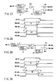
- FIG. 27 is a circuit diagram showing another example of the configuration of the trigger circuit for the write bit line driver/sinker in FIG. 11 ;
- FIG. 28 is a waveform diagram showing an example of operations of the trigger circuits in FIGS. 27 and 10 ;
- FIG. 29 is a circuit diagram of a trigger circuit for a write bit line driver/sinker used in an MRAM device according to a fourth embodiment
- FIG. 30 is a waveform diagram showing an example of operations performed by a combination of the trigger circuit in FIG. 29 with the trigger circuit in FIG. 10 ;
- FIG. 31 is a circuit diagram showing a variation of the trigger circuit for the write bit line driver/sinker shown in FIG. 29 ;
- FIG. 32 is a waveform diagram showing an example of operations performed by a combination of the trigger circuit in FIG. 31 with the trigger circuit in FIG. 10 ;
- FIG. 33 is a characteristic diagram showing an example of a distorted asteroid curve for an MTJ element
- FIG. 34 is a circuit diagram of a write bit line driver/sinker used in an MRAM device according to a fifth embodiment
- FIGS. 35A and 35B are circuit diagrams of a trigger circuit for the write bit line driver/sinker shown in FIG. 34 ;
- FIG. 36 is a waveform diagram showing an example of operations performed by a combination of the trigger circuits in FIGS. 35A and 35B with the trigger circuit in FIG. 10 ;
- FIG. 37 is a block diagram showing an example of the whole configuration of an MRAM device according to a sixth embodiment of the present invention.
- FIG. 38 is a circuit diagram of a write current waveform control circuit in FIG. 37 ;
- FIG. 39 is a circuit diagram of a trigger circuit for the write word line driver/sinker in FIG. 38 ;
- FIG. 40 is a circuit diagram of a trigger circuit for the write bit line driver/sinker in FIG. 38 ;
- FIG. 41 is a circuit diagram of a setting circuit in FIG. 37 ;
- FIG. 42 is a circuit diagram showing an example of the configuration of a register in FIG. 41 ;
- FIG. 43 is a circuit diagram showing another example of the configuration of the register in FIG. 41 ;
- FIG. 44 is a circuit diagram of a clamp potential generating circuit in FIG. 43 which generates a clamp potential
- FIG. 45 is a circuit diagram showing an example of the configuration of a decoder in a setting circuit in FIG. 41 ;
- FIG. 46 is a characteristic diagram showing the relationship between the temperature and pulse width observed if delay circuits composed of CMOS inverters are used as the delay circuits in the trigger circuit in FIGS. 39 and 40 ;
- FIG. 47 is a characteristic diagram showing the relationship between the temperature and pulse width observed if the current control type delay circuit in FIG. 13 controlled by the current control input source in FIG. 14 is used as each of the delay circuits in the trigger circuit in FIGS. 39 and 40 ;
- FIG. 48 is a characteristic diagram showing the relationship between the temperature and pulse width observed if the current control type delay circuit in FIG. 13 controlled by the current control input source in FIG. 16 is used as each of the delay circuits in the trigger circuit in FIGS. 39 and 40 ;
- FIG. 49 is a circuit diagram showing an example of the configuration of a current control type delay circuit that can be used as each of the delay circuits in the trigger circuit in FIGS. 39 and 40 ;
- FIG. 50 is a circuit diagram showing an example of the configuration of a current source circuit that supplies an input current to the delay circuit shown in FIG. 13 or 49 ;
- FIG. 51 is a circuit diagram showing another example of the configuration of the current source circuit that supplies an input current to the delay circuit shown in FIG. 13 or 49 ;
- FIG. 52 is a block diagram showing the whole configuration of an MRAM device according to a seventh embodiment of the present invention.
- FIG. 53 is a circuit diagram of a row decoder and write word line driver/sinker in FIG. 52 ;
- FIG. 54 is a circuit diagram of a column decoder and write bit line driver/sinker in FIG. 52 ;
- FIG. 55 is a circuit diagram showing an example of a write current waveform control circuit in FIG. 52 ;
- FIG. 56 is a circuit diagram of a write word line driver/sinker trigger circuit in FIG. 55 ;
- FIG. 57 is a circuit diagram of a write bit line driver/sinker trigger circuit in FIG. 55 ;
- FIG. 58 is a circuit diagram of waveform generating circuits in FIGS. 56 and 57 ;
- FIG. 59 is a waveform diagram showing examples of write word/bit line drive signals generated using the waveform generating circuit in FIG. 58 and write word/bit line currents controlled by these signals;
- FIG. 60 is a circuit diagram of a setting circuit shown in FIG. 58 and generating a current waveform control signal
- FIG. 61 is a circuit diagram of each of the decoders in the setting circuit shown in FIG. 60 ;
- FIG. 62 is a block diagram partly showing an MRAM device according to an eighth embodiment.
- FIG. 63 is a circuit diagram of a current source circuit used in FIG. 62 to output a current that is dependent on temperature;
- FIG. 64 is a characteristic diagram showing the relationship between the temperature of and a current from the current source circuit shown in FIG. 63 ;
- FIG. 65 is a circuit diagram showing another example of the current source circuit used in FIG. 62 to output a current that is dependent on temperature;
- FIG. 66 is a characteristic diagram showing the relationship between the temperature of and a current from the current source circuit shown in FIG. 65 ;
- FIG. 67 is a block diagram showing a DLS data path portion of a digital subscriber modem that is a first example of the application of the MRAM device;
- FIG. 68 is a block diagram showing a portion of a cellphone which implements a communication function, the cellphone being a second example of the application of the MRAM device;
- FIG. 69 is a plan view showing an example in which the MRAM device is applied to an MRAM card that houses media contents such as a Smart Media;
- FIG. 70 is a plan view showing an insertion type data transfer apparatus as an example of an electronic apparatus that uses the MRAM card;
- FIG. 71 is a sectional view corresponding to FIG. 70 ;
- FIG. 72 is a sectional view showing a fit-in type data transfer apparatus as another example of the electronic apparatus that uses the MRAM card.
- FIG. 73 is a sectional view showing a slide type data transfer apparatus as yet another example of the electronic apparatus that uses the MRAM card.
- FIG. 1 schematically shows the sectional structure of an MTJ element.
- the MTJ element has a structure in which one non-magnetic layer (tunnel barrier layer) 3 sandwiched between two magnetic layers 1 and 2 each composed of a ferromagnetic layer.
- the MTJ element stores “1” or “ 0 ” information depending on whether the orientations of magnetization in the two magnetic layers 1 and 2 are parallel or anti-parallel.
- an anti-ferromagnetic layer 4 is arranged adjacent to the magnetic layer 1 .
- the anti-ferromagnetic layer 4 is a member that fixes the orientation of the magnetization in the magnetic layer 1 so as to allow data to be easily rewritten by changing only the orientation of the magnetization in the magnetic layer 2 .
- the magnetic layer 1 with a fixed magnetization orientation is called a “fixed layer (or pinned layer)”.
- the magnetic layer 2 with a variable magnetization orientation is called a “free layer (or recording layer)”.
- FIGS. 2A and 2B show two states of the orientations of magnetization in the two magnetic layers 1 and 2 in the MTJ element shown in FIG. 1 .
- the tunnel resistance of the tunnel barrier film 3 sandwiched between the magnetic layers 1 and 2 , is lowest. In this case, a tunnel current is highest.
- the tunnel resistance of the tunnel barrier film 3 sandwiched between the magnetic layers 1 and 2 , is highest. In this case, the tunnel current is lowest.
- the two states in which the MTJ element has different resistance values correspond to the state in which logical “1” level data is stored (a “1” state) and the state in which logical “0” level data is stored (a “0” state), respectively.
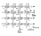
- FIG. 3 schematically shows an example of a planar layout of a cell array in which a plurality of MRAMs are two-dimensionally arranged in a row direction and a column direction.
- a plurality of write/read bit lines BL and a plurality of write word lines WWL are disposed so as to cross at right angles.
- MTJ elements 5 are disposed at the respective intersection points between the bit lines and the write word lines.
- Each MTJ element 5 is shaped like a rectangle the long sides of which extend along the write word lines WWL and the short sides of which extend along the bit lines BL. Magnetization is directed along the long sides of the rectangle.
- Each bit line BL is connected to one (reference numeral 1 or 2 in FIG. 1 ) of the magnetic layers of each of the plurality of MTJ elements 5 in the same row (or column).
- Each write word line WWL is arranged close to and opposite the other magnetic layer (reference numeral 2 or 1 in FIG. 1 ) of each of the plurality of MTJ elements 5 in the same column (or row).
- FIG. 4 is a sectional view showing an example of the structure of one memory cell in a cross section perpendicular to the write word lines.
- the memory cell is constructed by connecting an NMOS transistor as a read cell selection switch element in series with each MTJ element 5 in FIG. 3 .
- an impurity diffusion layer (N + ) that composes a drain region 61 or a source region 62 is selectively formed in a surface layer of a semi-conductor substrate composed of, for example, a P-type Si substrate.
- a gate electrode 64 is formed on a channel area via a gate oxide film 63 .
- Reference numerals 65 and 66 denote a first metal interconnect layer and a second metal interconnect layer, respectively.
- Reference numeral 67 denotes an MTJ connecting interconnect composed of a third metal interconnect layer.
- Reference numeral 68 denotes a contact that electrically connects the first metal interconnect layer 65 to the impurity diffusion layer (N + ).
- Reference numeral 69 denotes a contact that electrically connects the second metal interconnect layer 66 to the first metal interconnect layer 65 .
- Reference numeral 70 denotes a contact that electrically connects the third metal interconnect layer 67 to the second metal interconnect layer 66 .
- Reference numerals 50 and 71 denote an MTJ element and a fourth interconnect layer, respectively.
- Reference numeral 72 denotes a contact that electrically connects a fourth metal interconnect layer 71 to the MTJ element 5 .
- An interlayer insulating film is formed between each pair of interconnect layers.
- reference characters BL, WWL, SL, and RWL denote a write/read bit line, a write word line, a source line, and a read word line, respectively.
- the source line SL is connected to a ground potential.
- a write to the MTJ element 5 is achieved by conducting currents through the corresponding write word line WWL and bit line BL and using a combined magnetic field generated by the currents conducting through both interconnects to make the orientations of magnetization in the MTJ element 5 parallel or anti-parallel.
- a current flowing in a first direction or second direction opposite to the first direction depending on write data is conducted through the bit lines BL to generate a magnetic field Hx.
- a current flowing through a fixed direction is conducted through the write word lines WWL to generate a magnetic field Hy.
- the combined magnetic field generated is used to write information in the selected MTJ element 5 .
- the orientations in magnetization in the MTJ element are parallel.
- the orientations in magnetization in the MTJ element are anti-parallel.
- the corresponding read word line RWL is activated to turn on only the NMOSFET in FIG. 4 connected to the selected MTJ element.
- a current path is created.
- a current is conducted through the selected bit line BL to the source line SL.
- a current based on its resistance values flows. Information can be read by detecting this current value.
- FIG. 5 shows a TMR characteristics curve of the magnetic field applied of the MTJ element and the resistance value of the MTJ element.
- FIG. 6 shows an asteroid curve which shows the minimum magnetic magnitude to change the orientation of the free layer magnetization of the MTJ element.
- the resistance value of the MTJ element changes by, for example, about 17%.
- This change rate i.e. a ratio of the resistance difference between two states and the parallel state resistance is referred to as an “MR ratio”.
- the MR ratio varies depending on the properties of the magnetic layer in the MTJ element. At present, an MTJ element has the MR ratio of approximately 50% is available.
- the MTJ element is subjected to a magnetic field obtained by combining the magnetic field Hx in the easy-axis direction with the magnetic field Hy in the hard-axis direction.
- the magnitude of the magnetic field Hx in the easy-axis direction required to change the resistance value of the MTJ element also varies depend on the magnitude of the magnetic field Hy in the hard-axis direction. In the memory cells arranged as an array, this phenomenon can be utilized to write data only in the MTJ element arranged at the intersection point between the selected write word line WWL and the selected bit line BL.
- the orientation of the magnetization in the magnetic field of the MTJ element can be switched if the each magnitude of the magnetic field Hx in the easy-axis direction is larger than the magnitude of the magnetic field Hx in the easy-axis direction on the asteroid curve and the magnetic field Hy in the hard-axis direction is larger than the magnetic field Hy in the hard-axis direction on the asteroid curve, e.g. at the solid point in the figure. That is, data writes are enabled.
- the orientation of the magnetization in the magnetic field of the MTJ element cannot be switched if the magnitude of the magnetic field Hx in the easy-axis direction is smaller than the magnitude of the magnetic field Hx in the easy-axis direction on the asteroid curve or the magnetic field Hy in the hard-axis direction is smaller than the magnitude of the magnetic field Hy in the hard-axis direction on the asteroid curve, e.g. at the hollow point in the figure. That is, data writes are disabled.
- data writes to the MTJ element can be controlled by varying the magnitude of the combined magnetic field of the magnetic field Hx in the easy-axis direction and the magnetic field Hy in the hard-axis direction and varying the position of the magnitude of the combined magnetic field in an Hx-Hy plane.
- the MTJ element is subjected to only the magnetic field Hx in the easy-axis direction, i.e. only the magnetic field Hx induced by the write word line current or only the magnetic field Hy in the hard-axis direction, i.e. only the magnetic field Hy induced by the write bit line current, then the magnitude of the magnetic field is not located outside the asteroid curve. Consequently, data writes are disabled.
- the stabilized write characteristic is important particularly if the data stored in the MTJ element is different from the write data. In such a case, the direction of the magnetization in the recording layer of the MTJ element must be stably switched.
- the orientation of the magnetization in the free layer (recording layer) of the MTJ element can be switched by applying a specified combined magnetic field required to switch the magnetization, regardless of the direction of the switching (upward or downward).
- the necessary magnitude of the magnetic field Hy in the hard-axis direction alone to write one MTJ element is smaller than the necessary magnitude of the magnetic field Hy in the hard-axis direction to write the arbitrarily selected MTJ element by combining with the magnetic field Hx in the easy-axis direction, or the necessary magnitude of the magnetic field Hx in the easy-axis direction alone to write one MTJ element is smaller than the necessary magnitude of the magnetic field Hx in the easy-axis direction to write the arbitrarily selected MTJ element by combining with the magnetic field Hy in the hard-axis direction.
- the magnetic field generating from only the word line current or the bit line current causes a write. Accordingly, a write state is established by selecting only one of the word and bit lines.
- MTJ elements are arranged on a two-dimensional array as shown in FIG. 3 . Then, some MTJ elements are in a half-selected state in which a certain write word line WWL has been selected for them and the current flow through the write word line WL, whereas no write bit lines BLs have been selected for them and the no current flow through the write bit lines BLs.
- a data write occurs when such MTJ elements in the half-selected state are subjected to a magnetic field that causes only with the current through the write word line WWL, if the applied magnetic field is larger than the magnetic field on the asteroid curve shown the switching characteristics of those MTJs. Therefore, there is a limit to the maximum current that can be conducted through the write word line WWL. Above discussion is applied not only for the write word line but also for the write bit line.
- FIG. 7 is a block diagram shows an example of the whole configuration of an MRAM device according to a first embodiment of the present invention.
- An MRAM 11 may in itself constitute one memory chip or may be one block within a chip which block has a particular function.
- a memory cell array (data cell) 12 has a function of actually storing data.
- a reference cell array 13 has a function of determining a reference level used to determine read data, during a data read operation.
- a row decoder and driver 14 composed of a row decoder and write word line driver, and a row decoder and read word line driver is arranged at one of the two ends of a cell array in the X direction (easy-axis direction), the cell array being composed of the memory cell array 12 and the reference cell array 13 .
- a write word line sinker 15 is arranged at the other end.
- the row decoder and driver 14 has a function of operating during a data write to select one of a plurality of write word lines, for example, on the basis of a row address signal and supplying a write current to the selected write word line.
- the write word line sinker 15 has a function of operating during a data write to, for example, absorb a write current supplied to the selected write word line.
- the row decoder and driver 14 has a function of operating during a data read to select one of a plurality of read word lines, for example, on the basis of a row address signal and supplying a read current to the selected read word line.
- the write word line may also be used as a read word line.
- a sense amplifier 20 detects the read current through the read word line to determine read data.
- a column decoder and write bit line driver/sinker 16 A is arranged at one of the two ends of the memory array 12 in the Y direction (hard-axis direction).
- a column decoder and write bit line driver/sinker 17 A including a column transfer gate and a column decoder is arranged at the other end.
- the column decoder and write bit drivers/sinkers 16 A and 17 A have a function of operating during a data write to select one of a plurality of write bit lines or data select lines, for example, on the basis of a column address signal and supplying the selected write bit line with a write current having an orientation based on write data.
- the column transfer gate and the column decoder have a function of operating during a read to connect electrically a data selection line selected by the column address signal to the sense amplifier 20 .
- a reference cell column decoder and write bit line driver/sinker 16 B is arranged at one of the two ends of the reference cell array 13 in the Y direction.
- a reference cell column decoder and write bit line driver/sinker 17 B including a column transfer gate and a column decoder is arranged at the other end.
- the reference cell column decoder and write bit line drivers/sinkers 16 B and 17 B have a function of storing reference data in the reference cell array 13 .
- the column transfer gate and the column decoder have a function of operating during a read to read reference data from the reference cell array and transfer the data to the sense amplifier 20 .
- An address receiver 18 receives an address signal and transfers, for example, a row address signal to the row decoder and driver 14 , while transferring a column address signal to the column decoder and write bit line drivers/sinkers 16 A and 17 A.
- a data input receiver 19 transfers write data to the column decoder and write bit line drivers/sinkers 16 A and 17 A.
- a data output driver 21 outputs read data detected by the sense amplifier 20 to equipment located outside the MRAM chip.
- a control circuit 22 receives a chip enable signal /CE, a write enable signal /WE, and an output enable signal /OE to generate various control signals that control the operation of the whole MRAM. For a data write operation, the control circuit 22 provides a write signal WRITE to a write current waveform control circuit 24 .
- the write current waveform control circuit 24 On receiving the write signal WRITE, the write current waveform control circuit 24 generates a write word line drive signal WWLDRV, a write word line sink signal WWLSNK, a write bit line drive signal WBLDRV, and a write bit line sink signal WBLSNK.
- the write word line drive signal WWLDRV is supplied to the row decoder and driver 14 .
- the write word line sink signal WWLSNK is supplied to the write word line sinker 15 .
- the write bit line drive signal WBLDRV and the write bit line sink signal WBLSNK are supplied to the column decoder and write bit line drivers/sinkers 16 A and 17 A.
- the row decoder and driver 14 conducts a write current through the write word line selected by the row address signal.
- the write word line sinker 15 and the column decoder and write bit line drivers/sinkers 16 A and 17 A conduct a write current through the write bit line selected by the column address signal.
- the potentials across the write word/bit lines can be completely zeroed by, for example, allowing the sink signals WWLSNK and WBLSNK to change from “H” to “L” after the drive signals WWLDRV and WBLDRV have changed from “H” to “L”.
- the write current waveform control circuit 24 has a function of adjusting the pulse width of a pulse-like write current in accordance with temperature in order to prevent miswrites.
- control is provided such that the pulse width of the write current (the time for which the write current is applied) decreases consistently with increasing temperature.
- control may be provided by combining the variation of the pulse width of the write current with the variation of the magnitude of the write current.
- a switching magnetic field required to switch the magnetization in the MTJ element from a parallel state to an anti-parallel state differs from a switching magnetic field required to switch the magnetization in the MTJ element from the anti-parallel state to the parallel state
- control is provided such that the pulse width of the write current is changed in accordance with the write data so as to reduce the pulse width of the smaller switching magnetic field. This will be described below in detail.
- FIG. 8 shows a specific example of circuits in one row of the row decoder and driver 14 and write word line sinker 15 in FIG. 7 .
- One row of the row decoder and write word line driver 14 is composed of a NAND gate circuit NAD 1 and a P channel MOS transistor WS 1 .
- the write word line drive signal WWLDRV and a row address signal composed of a plurality of bits are input to the NAND gate circuit NAD 1 .
- the row address signal varies with rows.
- One row of the write word line sinker 15 is composed of an N channel MOS transistor TN 1 .
- a source of the N channel MOS transistor TN 1 is connected to a ground node VSS. Its drain is connected to the other end of the write word line WWLi.
- the write word line sink signal WWLSNK is input to a gate of the N channel MOS transistor TN 1 .
- the write word line drive signal WWLDRV changes to “H”.
- all the bits of the row address signal change to “H”. That is, for the selected row i, an output signal from the NAND circuit NAD 1 changes to “L”. Accordingly, the P channel MOS transistor WS 1 is turned on to supply the write word line WWLi with a write word line current with a predetermined value.
- the potential across the write word line WWLi can be completely zeroed after a write operation. This is convenient for initialization.
- FIG. 9 shows an example of circuits in one column of the column decoder and write bit drivers/sinkers 16 A and 17 A in FIG. 7 .
- One column of the column decoder and write bit line driver/sinker 16 A is composed of a NAND gate circuit NAD 2 , an AND gate circuit AD 1 , a P channel MOS transistor BS 1 , and an N channel MOS transistor BN 0 .
- the write bit line drive signal WBLDRV, a column address signal composed of a plurality of bits, and write data DATA are input to the AND gate circuit AD 2 .
- the column address signal varies with columns i.
- the write bit line sink signal WBLSNK, a column address signal composed of a plurality of bits, and an inversion data bDATA of the write data are input to the AND gate circuit AD 1 .
- One column of the column decoder and write bit line driver/sinker 17 A is composed of a NAND gate circuit NAND 3 , an AND gate circuit AD 2 , a P channel MOS transistor BS 2 , and an N channel MOS transistor BN 1 .
- the write bit line drive signal WBLDRV, a column address signal composed of a plurality of bits, and the inversion data bDATA of the write data are input to the NAND gate circuit NAD 3 .
- a gate of the P channel MOS transistor BS 2 is connected to an output terminal of the NAND gate circuit NAD 3 . Its source is connected to the power node VDD. Its drain is connected to the other end of the write bit line WBLi.
- the write bit line sink signal WBLSNK, a column address signal composed of a plurality of bits, and the write data DATA are input to the AND gate circuit AD 2 .
- a gate of the N channel MOS transistor BN 1 is connected to an output terminal of the AND gate circuit AD 2 . Its source is connected to the ground node VSS. Its drain is connected to the other end of the write bit line WBLi.
- both the write bit line drive signal WBLDRV and the write bit line sink signal WBLSNK change to “H”.
- all the bits of the column address signal change to “H”.
- a current flows through the write bit line between the column decoder and write bit line driver/sinker 16 A and the column decoder and write bit line driver/sinker 17 A.
- the magnitude of the current through the write bit line is determined by the P channel MOS transistor BS 1 and the P channel MOS transistor BS 2 .
- the potential across the write bit line WBLi can be completely zeroed after a write operation. This is convenient for initialization.
- FIG. 10 shows an example of a trigger circuit for the write word line driver/sinker that generates a write word line drive signal WWLDRV and a write word line sink signal WWLSNK, shown in FIG. 8 .
- This trigger circuit is composed of a WWLDRV signal generating circuit 25 X and a WWLSNK signal generating circuit 25 Y.
- the WWLDRV signal generating circuit 25 X is composed of a NAND gate circuit ND 1 , a delay circuit A, and inverters IV 1 and IV 2 .
- the WWLDRV signal generating circuit 25 X generates a write word line drive signal WWLDRV on the basis of a write signal WRITE and supplies this signal to the write word line driver.
- the write signal WRITE is an internal control signal indicating that a write is to be started. In a write mode, the write signal WRITE is “H”.
- the WWLSNK signal generating circuit 25 Y is composed of a delay circuit 27 and a NAND gate circuit ND 2 .
- the WWLSNK signal generating circuit 25 Y generates a write word line sink signal WWLSNK on the basis of an output signal from the NAND gate circuit ND 1 in the WWLDRV signal generating circuit 25 X and supplies this signal to the write word line sinker.
- FIG. 11 shows an example of a trigger circuit for the write bit line driver/sinker that generates a write bit line drive signal WBLDRV and a write bit line sink signal WBLSNK, shown in FIG. 9 .
- This trigger circuit is composed of a WBLDRV signal generating circuit 26 X and a WBLSNK signal generating circuit 26 Y.
- the WBLDRV signal generating circuit 26 X is composed of a NAND gate circuit ND 3 , a delay circuit B, and inverters IV 3 and IV 4 .
- the WBLDRV signal generating circuit 26 X generates a write bit line drive signal WBLDRV on the basis of the write signal WRITE and supplies this signal to the write bit line driver.
- the WBLSNK signal generating circuit 26 Y is composed of a delay circuit 28 and a NAND gate circuit ND 4 .
- the WBLSNK signal generating circuit 26 Y generates a write bit line sink signal WBLSNK on the basis of an output signal from the NAND gate circuit ND 3 in the WWLDRV signal generating circuit 26 X and supplies this signal to the write bit line sinker.
- the write word line drive signal WWLDRV, the write bit line drive signal WBLDRV, the write word line sink signal WWLSNK, and the write bit line sink signal WBLSNK change almost simultaneously from “L” to “H”.
- FIG. 12 shows an example of operation waveforms of the trigger circuits shown in FIGS. 10 and 11 .
- the delay circuits A and B in FIGS. 10 and 11 determine the pulse widths of output signals in accordance with respective delay times tA and tB and control the pulse widths of the output signals on the basis of the temperature dependence of the delay times.
- the delay circuits A and B thus control the pulse widths of write currents supplied to the write word line driver/sinker and the write bit line driver/sinker, respectively.
- the delay circuits 27 and 28 in FIGS. 10 and 11 determine intervals t 27 and t 28 , respectively, corresponding to the periods after the write signal WRITE has changed from “H” to “L” and the write word line drive signal WWLDRV or write bit line drive signal WBLDRV has changed from “H” to “L” and before the write word line sink signal WWLSNK or write bit line sink signal WBLSNK changes from “H” to “L”.
- the intervals t 27 and t 28 are periods required to set the potential across the write word line WWLi or the write bit line WBLi to 0V.
- FIG. 13 shows an example of a current control type delay circuit.
- the delay time decreases in proportion to a current Isource generated by a current source. Accordingly, when this delay circuit is used as each of the delay circuits A and B in FIGS. 10 and 11 , respectively, the pulse width of an output signal from the trigger circuit decreases in proportion to the amount of current.
- FIG. 14 shows an example of a current source circuit that generates a current Isource substantially independent of temperature.
- This current source circuit is composed of a BGR (Band Gap Reference) circuit.
- the current source circuit eliminates the dependence on temperature by adding up a current I 1 obtained by copying a current from a first current source 81 the amount of which decreases in proportion to temperature and a current I 2 obtained by copying a current from a second current source 82 characterized in that the amount of current increases in proportion to temperature.
- FIG. 15 is a characteristic diagram showing the temperature dependence of the circuit in FIG. 14 .
- a current source circuit that outputs a current having a value increasing consistently with temperature may be used to provide a current input to the current control type delay circuit shown in FIG. 13 .
- the delay time in the delay circuit decreases in keeping with increasing temperature.
- this delay circuit is used as each of the delay circuits A and B in FIGS. 10 and 11 , respectively, the pulse width of an output signal from the trigger circuit decreases in proportion to the amount of input current supplied by the current source circuit.
- FIG. 16 shows an example of a current source circuit that outputs a current having a value increasing in keeping with temperature.
- This current source circuit realizes the characteristic that the value of the output current increases consistently with temperature, by subtracting the current I 1 obtained by copying a current from the first current source 81 characterized in that the value of the current decreases in proportion to temperature from the current I 2 obtained by copying a current from the second current source 82 which increases in proportion to temperature.
- FIG. 17 indicates the temperature dependence of the circuit in FIG. 16 .
- a current source circuit that outputs a current exhibiting its temperature dependency as a folded line may be used to provide a current input to the current control type delay circuit shown in FIG. 13 .
- the dependency of the delay time on temperature can be exhibited as a folded line.
- FIG. 18 shows an example of a current source circuit that outputs a current exhibiting its temperature dependence as a folded line. Further, FIGS. 19A and 19B show the signal waveform and temperature dependence of the current source circuit in FIG. 18 .
- the current source circuit in FIG. 18 is composed of a first current source 121 and a second current source 122 each of which provides a current having a value increasing in proportion to temperature, a third current source 123 that provides a current having a value decreasing in proportion to temperature, a combinatorial circuit 124 that can select one of the combinations of outputs from the above three circuits, and a temperature sensor circuit 125 that detects temperature to control the combination.
- the combinatorial circuit 124 outputs a current I 1 obtained by copying a current through the first current source 121 .
- the combinatorial circuit 124 adds a current I 2 obtained by copying a current through the second current source 122 to the current I 1 obtained by copying the current through the first current source 121 , then subtracts a current I 3 obtained by copying a current through the third current source 123 , from the synthetic current (I 1 +I 2 ), and finally outputs the resultant current.
- An example of the temperature sensor circuit 125 can be implemented by combining an output current from the circuit providing a current having a value increasing in proportion to temperature with an output current from the circuit providing a current having a value decreasing in proportion to temperature.
- the temperature sensor circuit 125 in FIG. 18 outputs “H” and “L” as complementary binary signals Vtemp and bVtemp, for example, as shown in FIG. 19A .
- the complementary binary signals Vtemp and bVtemp change to “L” and “H”, respectively.
- a switch point (temperature T 0 ) for the characteristics of the temperature sensor circuit 125 is set on the basis of the ratio of the amount of current output by the circuit providing a current having a value increasing in proportion to temperature to the amount of current output by the circuit providing a current having a value decreasing in proportion to temperature.
- the temperature dependence of an input current to the current control type delay circuit shown in FIG. 13 can be exhibited as a line with two folds.
- the temperature dependence of the delay time can be exhibited as a line with two folds.
- FIG. 20 shows an example of a current source circuit that outputs a current exhibiting its temperature dependence as a line with two folds. Further, FIGS. 21A and 21B show the signal waveform and temperature dependence of the current source circuit in FIG. 20 .
- the current source circuit in FIG. 20 is composed of a first current source 141 , a second current source 142 , and a fourth current source 144 each of which provides a current having a value increasing in proportion to temperature, a third current source 143 and a fifth current source 145 each of which provides a current having a value decreasing in proportion to temperature, a combinatorial circuit 146 that allows the selection of a combination of outputs from the above five circuits, and a first temperature sensor circuit 147 and a second temperature sensor circuit 148 each of which detects temperature to control the combination.
- the combinatorial circuit 146 outputs a current I 1 obtained by copying a current through the first current source 141 .
- the combinatorial circuit 146 adds a current I 2 obtained by copying a current through the second current source 142 to the current I 1 obtained by copying the current through the first current source 141 , then subtracts a current I 3 obtained by copying a current through the third current source 143 , from the synthetic current (I 1 +I 2 ), and finally outputs the resultant current (I 1 +I 2 ⁇ I 3 ).
- the combinatorial circuit 146 adds a current I 4 obtained by copying a current through the fourth current source 144 to the current (I 1 +I 2 ⁇ I 3 ), then subtracts a current I 5 obtained by copying a current through the fifth current source 145 , from the synthetic current (I 1 +I 2 ⁇ I 3 +I 4 ), and finally outputs the resultant current (I 1 +I 2 ⁇ I 3 +I 4 ⁇ I 5 ).
- a signal Vtemp 1 is “H” at the first temperature T 1 or lower, while the signal Vtemp 1 is “L” in the temperature region exceeding the temperature T 1 .
- the first temperature sensor circuit 147 complementary binary signals Vtemp 1 and Vtemp 2 on the basis of these signals. These complementary binary signals are used to switch and control paths for the output current I 4 from the fourth current source 144 and the output current I 5 from the fifth current source 145 .
- FIG. 22 shows the relationship between temperature and the pulse width of the signal WWLDRV or WBLDRV observed if CMOS inverter circuits are used as each of the delay circuits A and B.
- the characteristic obtained is that the pulse width increases consistently with temperature.
- FIG. 23 shows the relationship between temperature and the pulse width of the signal WWLDRV or WBLDRV observed if the current control type delay circuit in FIG. 13 using the current source circuit shown in FIG. 14 is used as each of the delay circuits A and B.
- the characteristic obtained in that the pulse width is independent of temperature.
- FIG. 24 shows the relationship between temperature and the pulse width of the signal WWLDRV or WBLDRV observed if the current control type delay circuit in FIG. 13 using the current source circuit shown in FIG. 16 is used as each of the delay circuits A and B. In this case, the characteristic obtained in that the pulse width decreases with increasing temperature.
- FIG. 25 shows the relationship between temperature and the pulse width of the signal WWLDRV or WBLDRV observed if the current control type delay circuit in FIG. 13 using the current source circuit shown in FIG. 18 is used as each of the delay circuits A and B.
- FIG. 26 shows the relationship between temperature and the pulse width of the signal WWLDRV or WBLDRV observed if the current control type delay circuit in FIG. 13 using the current source circuit shown in FIG. 20 is used as each of the delay circuits A and B.
- the MRAM device is characterized by having a function of appropriately setting the temperature characteristics of the delay circuit A in the write word line driver/sinker trigger circuit and the delay circuit B in the write bit line driver/sinker trigger circuit so that the pulse width of the pulse-like write current is independent of temperature or varies with temperature. This prevents miswrites in high temperature regions.
- the temperature dependence of the delay circuit A used in the write word line driver/sinker trigger circuit shown in FIG. 10 differs from the temperature dependence of the delay circuit B used in the write bit line driver/sinker trigger circuit shown in FIG. 11 . Specific examples will be described below.
- the current sources in these two delay circuits have difference temperature dependences.
- the two current sources with different temperature dependences can be implemented by making the amount of current from the first current source 81 , providing a current having a value decreasing in proportion to temperature, different from the amount of current from the second current source 82 , providing a current having a value increasing in proportion to temperature, each current source being provided in the current source circuit shown in FIG. 16 .
- the pulse width of a write current from the write word line driver/sinker shown in FIG. 8 can be made different from the pulse width of the write current from the write bit line driver/sinker shown in FIG. 9 .
- the temperature dependence shown in FIG. 15 may be exhibited as a line with one or more folded points.
- U.S. Pat. No. 6,081,445 describes a method of reproducibly rewriting the direction of magnetization in the MTJ element.
- This method writes data by applying the magnetic field Hy in the hard-axis direction to the MTJ element to set the direction of magnetization in the magnetic domain at the end of the recording layer and then applying the magnetic field Hx in the easy-axis direction. That is, a write current is conducted through the write word line and then a write current is conducted through the write bit line.
- the switching of magnetization in the recording layer of the MTJ element is known to proceed from the end of a ferromagnetic layer.
- the above method increases the time required for a write. This means that a miswrite stress is more likely to occur in a half-selected memory cell to which only the magnetic field from the write word line has been applied. Thus, undesirably, the magnetization is easily switched in high temperature regions.
- the configuration of the write bit line driver/sinker trigger circuit shown in FIG. 11 is partly changed. This will be specifically described below.
- FIG. 27 shows the specific configuration of the write bit line driver/sinker trigger circuit.
- This circuit is configured partly differently from the circuit shown in FIG. 11 . That is, the trigger circuit in FIG. 27 is the same as the trigger circuit shown in FIG. 11 except that the delay circuit B is replaced with a delay circuit C and that the write signal WRITE is transmitted to one of the inputs of the NAND gate circuit ND 3 via the delay circuit C.
- the same components as those in FIG. 11 are denoted by the same reference numerals.
- FIG. 28 shows an example of operation waveforms obtained if the write bit line driver/sinker trigger circuit in FIG. 27 is combined with the write word line driver/sinker trigger circuit in FIG. 10 .
- reference characters tA and tC denote a delay time in the delay circuit A and a delay time in the delay circuit C, respectively.
- Reference character tAC denotes a delay time determined by the difference in delay time between the delay circuits A and C.
- Reference character t 28 denotes a delay time in the delay circuit 28 .
- the delay circuit C is provided, so that the level of an output signal from the delay circuit C changes after an output signal from the write word line driver/sinker trigger circuit shown in FIG. 10 has changed. Furthermore, the delay circuit C has a temperature dependence such that the delay time decreases in high temperature regions. Consequently, the temperature dependence of the pulse width of an output signal from the trigger circuit in FIG. 27 is different from the temperature dependence of the pulse width of an output signal from the write word line driver/sinker trigger circuit shown in FIG. 10 . This reduces the difference between the time when the output signal from the trigger circuit in FIG. 27 changes and the time when the output signal from the trigger circuit in FIG. 10 changes. It is thus possible to allow the write bit line driver/sinker to start the application of a magnetic field in the easy-axis direction earlier.
- the delay circuit C can be provided with a temperature dependence such that the delay time decreases in high temperature regions, by, for example, using the current control type delay circuit shown in FIG. 13 and setting the temperature dependence of the current Isource, supplied to this delay circuit, so that the delay time decreases in high temperature regions.
- the write bit line driver/sinker trigger circuit shown in FIG. 11 is replaced with a write bit line driver/sinker trigger circuit such as the one shown in FIG. 11
- This trigger circuit is the same as the trigger circuit shown in FIG. 11 except that the write signal WRITE is transmitted to one of the inputs of the NAND gate circuit ND 3 and to the delay circuit A, via the delay circuit C.
- the same components as those in FIG. 11 are denoted by the same reference numerals.
- FIG. 30 shows an example of operation waveforms obtained if the write bit line driver/sinker trigger circuit in FIG. 29 is combined with the write word line driver/sinker trigger circuit in FIG. 10 .
- reference characters tA and tB denote a delay time in the delay circuit A and a delay time in the delay circuit B, respectively.
- Reference characters tC and t 28 denote a delay time in the delay circuit C and a delay time in the delay circuit 28 , respectively.
- the delay circuit C is provided, so that the pulse width of an output signal from the trigger circuit decreases. Further, the output signal changes after an output signal from the write word line driver/sinker trigger circuit shown in FIG. 10 has changed.
- the delay circuit C has a temperature dependence such that the delay time decreases in high temperature regions. Consequently, the temperature dependence of the pulse width of an output signal from the trigger circuit in FIG. 29 is different from the temperature dependence of the pulse width of an output signal from the trigger circuit shown in FIG. 10 . This reduces the difference between the time when the output signal from the trigger circuit in FIG. 29 changes and the time when the output signal from the trigger circuit in FIG. 10 changes. It is thus possible to allow the write bit line driver/sinker shown in FIG. 9 to start the application of a magnetic field in the easy-axis direction earlier.
- the interval between the time to start applying a magnetic field in the hard-axis direction and the time to start applying a magnetic field in the easy-axis direction is different from the interval between the time to end the application of the magnetic field in the hard-axis direction and the time to end the application of the magnetic field in the easy-axis direction.
- FIG. 31 shows the configuration of a write bit line driver/sinker trigger circuit according to the present variation.
- the trigger circuit in FIG. 31 is the same as the trigger circuit shown in FIG. 11 except that the write signal WRITE is transmitted to one of the inputs of the NAND gate circuit ND 3 via the delay circuit C.
- the same components as those in FIG. 11 are denoted by the same reference numerals.
- FIG. 32 shows an example of operation waveforms obtained if the write bit line driver/sinker trigger circuit in FIG. 31 is combined with the write word line driver/sinker trigger circuit in FIG. 10 .
- reference characters tA and tC denote a delay time in the delay circuit A and a delay time in the delay circuit C, respectively.
- Reference character tAB denotes a delay time determined by the difference in delay time between the delay circuits A and B.
- Reference character tBC denotes a delay time determined by the difference in delay time between the delay circuits B and C.
- Reference character t 28 denotes a delay time in the delay circuit 28 .
- the temperature dependence of the pulse width of an output signal from the trigger circuit in FIG. 31 is dependent on the temperature dependence of the delay circuit C. It is different from the temperature dependence of the pulse width of an output signal from the write word line driver/sinker trigger circuit in FIG. 10 . Furthermore, the temperature dependence of the delay circuit C in the trigger circuit in FIG. 31 affects the pulse width of an output signal from the write bit line driver/sinker shown in FIG. 9 in order to conduct a current through the write bit line.
- the asteroid curve for the MTJ element may be shifted in the easy-axis direction owing to a magnetic stray field from the fixed layer in the MTJ element or the ferromagnetic coupling with the fixed and the recording layer causing by the surface roughness of the fixed and recording layers which lie opposite the tunnel barrier film.
- FIG. 33 shows an example of a distorted asteroid curve for the MTJ element.
- a combined magnetic field F 1 is larger than the switching threshold magnetic field shown in the asteroid curve, the combined magnetic field F 1 being composed of a magnetic field in the easy-axis direction obtained if a write current is applied to the write bit line in a first direction and a magnetic field in the hard-axis direction obtained if a write current is applied to the write word line in a specified direction.
- a combined magnetic field F 2 is smaller than the switching threshold magnetic field shown in the asteroid curve, the combined magnetic field F 2 being composed of a magnetic field in the easy-axis direction obtained if a write current of the same value is applied to the write bit line in the direction opposite to the first direction and a magnetic field in the hard-axis direction obtained if the write current is applied to the write word line in the specified direction.
- writes are disabled unless the value of the required write current is varied depending on the write data, i.e. the direction of the write current.
- the pulse width of the pulse-like current, flowing through the write bit line is varied depending on the direction of the write current which is required to generates a magnetic field in the easy-axis direction. Furthermore, as in the case with the MRAM device according to the first embodiment, the pulse width is dependent on temperature.
- FIG. 34 shows the configuration of circuits in the write bit line drivers/sinkers 16 A and 17 A used in the MRAM device according to the fifth embodiment.
- write bit line drivers/sinkers 16 A and 17 A are the same as the write bit line driver/sinker previously described with reference to FIG. 9 except for the use of control signals WBLDRV 1 and WBLSNK 1 for a first direction of the write current and control signals WBLDRV 2 and WBLSNK 2 for a second direction of the write current.
- FIGS. 35A and 35B shows an example of the configuration of a trigger circuit for the write bit line driver/sinker in FIG. 34 .
- FIG. 36 shows an example of operation waveforms obtained if the write bit line driver/sinker trigger circuits in FIGS. 35A and 35B are combined with the write word line driver/sinker trigger circuit in FIG. 10 .
- reference characters tB 1 and tB 2 denote a delay time in a delay circuit B 1 and a delay time in a delay circuit B 2 , respectively.
- Reference character t 28 denotes a delay time in the delay circuit 28 .
- the first trigger circuit 261 shown in FIG. 35A generates control signals WBLDRV 1 and WBLSNK 1 for the first direction.
- the second trigger circuit 262 shown in FIG. 35B generates control signals WBLDRV 2 and WBLSNK 2 for the second direction.
- Each of the two trigger circuits 261 and 262 are the same as the trigger circuit previously described with reference to FIG. 11 except that the corresponding delay circuits B 1 and B 2 use different delay times.
- the delay time in the delay circuit provided in one of the trigger circuits which must increase a write current is set to be longer than the delay circuit in the other trigger circuit, e.g. the delay circuit B 2 , provided in the trigger circuit 262 .
- the fifth embodiment may be combined with one of the previously described first to fourth embodiments.
- the pulse width and temperature dependence of a write current can be adjusted by enabling the programmable setting of timings for starting and ending the supply of write currents to the write word line/bit line.
- FIG. 37 shows the whole configuration of the MRAM device according to the sixth embodiment.
- This MRAM device is the same as the MRAM device according to the first embodiment except that (1) a setting circuit 23 is added and (2) the write current waveform control circuit 24 provides different functions.
- the same components as those in FIG. 7 are denoted by the same reference numerals. Thus, their description is omitted.
- the newly added setting circuit 32 is provided with programming elements composed of, for example, laser blow fuses, MTJ elements, anti-fuses that destroy the tunnel barriers of MTJ elements, or the like. Setting data is preprogrammed in these programming elements.
- the write current waveform control circuit 24 may be supplied with setting data input through, for example, a data I/O terminal or an address terminal.
- FIG. 38 shows an example of the write current waveform control circuit 24 in FIG. 37 .
- the write current waveform control circuit 24 is composed of a write word line driver/sinker trigger circuit 25 and a write bit line driver/sinker trigger circuit 26 .
- the write current waveform control circuit 24 generates a write word line drive signal WWLDRV, a write word line sink signal WWLSNK, a write bit line drive signal WBLDRV, and a write bit line sink signal WBLSNK.
- the write word line driver/sinker trigger circuit 25 generates a write word line drive signal WWLDRV and a write word line sink signal WWLSNK on the basis of the write signal WRITE and timing control signals WS ⁇ 0> to WS ⁇ 3> and bWS ⁇ 0> to bWS ⁇ 3>.
- the write bit line driver/sinker trigger circuit 26 generates a write bit line drive signal WBLDRV and a write bit line sink signal WBLSNK on the basis of the write signal WRITE and timing control signals BS ⁇ 0> to BS ⁇ 3> and bBS ⁇ 0> to bBS ⁇ 3>.
- the write signal WRITE signal changes to “H” for a write operation.
- the timing control signals WS ⁇ 0> to WS ⁇ 3> and bWS ⁇ 0> to bWS ⁇ 3> determine timings for starting and ending the supply of a write current to the write word line WWLi, i.e. timings used to change the write word line drive signal WWLDRV and the write word line sink signal WWLSNK to “H” or “L”.
- the timing control signals BS ⁇ 0> to BS ⁇ 3> and bBS ⁇ 0> to bBS ⁇ 3> determine timings for starting and ending the supply of a write current to the write bit line WBLi, i.e. timings used to change the write bit line drive signal WBLDRV and the write bit line sink signal WBLSNK to “H” or “L”.
- the setting circuit 23 generates timings control signals WS ⁇ 0> to WS ⁇ 3>, bWS ⁇ 0> to bWS ⁇ 3>, BS ⁇ 0> to BS ⁇ 3>, and bBS ⁇ 0> to bBS ⁇ 3>.
- FIG. 39 shows an example of the write word line driver/sinker trigger circuit 25 in FIG. 38 .
- the write word line driver/sinker trigger circuit 25 is composed of a current supply start/end timing determining circuit 25 X that determines timings for starting and ending the supply of a write current and a current sink timing determining circuit 25 Y that determines a timing for sinking a write current.
- the current supply start/end timing determining circuit 25 X determines a timing for changing the write word line drive signal WWLDRV to “H” after the write signal WRITE has changed to “H”. It also determines a timing for changing the write word line drive signal WWLDRV to “L” after the write signal WRITE has changed to “L”.
- the current supply start/end timing determining circuit 25 X is composed of a plurality of, in the present example, four delay circuits DWS ⁇ 0> to DWS ⁇ 3>, transfer gates TGWS ⁇ 0> to TGWS ⁇ 3>, and inverters I 1 and I 2 .
- the delay circuits DWS ⁇ 0> to DWS ⁇ 3> have different amounts of delay with respect to the write signal WRITE as an input signal.
- the amounts of delay in the delay circuits DWS ⁇ 0> to DWS ⁇ 3> may be set to have specified differences or to vary regularly or randomly.
- the write signal WRITE is output by the write word line driver/sinker trigger circuit 25 via the selected delay circuit DWS ⁇ j> as the write word line drive signal WWLDRV.
- the four delay circuits DWS ⁇ 0> to DWS ⁇ 3> are provided.
- the number of selectable delay amounts increases consistently with the number of delay circuits.
- An increased number of selectable delay amounts enable the precise control of the timings for starting and ending the supply of a write current.
- the number of timing control signals used to select one of the delay circuits also increases.
- the current sink timing determining circuit 25 Y is composed of the NAND gate ND 1 and the delay circuit 27 .
- the current sink timing determining circuit 25 Y changes the write word line sink signal WWLSNK to “H” at almost the same time when the write word line drive signal WWLDRV changes to “H” and then after a delay time determined by the delay circuit 27 , changes the write word line sink signal WWLSNK to “L”.
- FIG. 40 shows an example of the write bit line driver/sinker trigger circuit 26 in FIG. 38 .
- the write bit line driver/sinker trigger circuit 26 is composed of a current supply start/end timing determining circuit 26 X that determines timings for starting and ending the supply of a write current and a current sink timing determining circuit 26 Y that determines a timing for sinking a write current.
- the current supply start/end timing determining circuit 26 X determines a timing for changing the write bit line drive signal WBLDRV to “H” after the write signal WRITE has changed to “H”. It also determines a timing for changing the write bit line drive signal WBLDRV to “L” after the write signal WRITE has changed to “L”.
- the current supply start/end timing determining circuit 26 X is composed of a plurality of, in the present example, four delay circuits DBS ⁇ 0> to DBS ⁇ 3>, transfer gates TGBS ⁇ 0> to TGBS ⁇ 3>, and inverters I 3 and I 4 .
- the delay circuits DBS ⁇ 0> to DBS ⁇ 3> have different amounts of delay with respect to an input signal, i.e. the write signal WRITE.
- the amounts of delay in the delay circuits DBS ⁇ 0> to DBS ⁇ 3> may be set to have specified differences or to vary regularly or randomly.
- the write signal WRITE is output by the write bit line driver/sinker trigger circuit 25 via the selected delay circuit DBS ⁇ j> as the write bit line drive signal WBLDRV.
- the four delay circuits DBS ⁇ 0> to DBS ⁇ 3> are provided.
- the number of selectable delay amounts increases consistently with the number of delay circuits.
- An increased number of selectable delay amounts enable the precise control of the timings for starting and ending the supply of a write current.
- the number of timing control signals used to select one of the delay circuits also increases.
- the current sink timing determining circuit 26 Y is composed of the NAND gate ND 2 and the delay circuit 28 .
- the current sink timing determining circuit 26 Y changes the write bit line sink signal WBLSNK to “H” at almost the same time when the write bit line drive signal WBLDRV changes to “H” and then after a delay time determined by the delay circuit 28 , changes the write bit line sink signal WBLSNK to “L”.
- the setting circuit 23 which generates timing control signals WS ⁇ 0> to WS ⁇ 3>, bWS ⁇ 0> to bWS ⁇ 3>, BS ⁇ 0> to BS ⁇ 3>, and bBS ⁇ 0> to bBS ⁇ 3>, shown in FIGS. 38 to 40 .
- FIG. 41 shows an example of the setting circuit 23 in FIG. 37 .
- the setting circuit 23 is composed of registers Reg ⁇ 0> to Reg ⁇ 3> in which setting data used to determine the timings for starting and ending the supply of a write current is programmed and decoders DecWS ⁇ 0> to DecWS ⁇ 3> and DecBS ⁇ 0> to DecBS ⁇ 3> which decode output signals TD ⁇ 0> to TD ⁇ 3> and bTD ⁇ 0> to bTD ⁇ 3>, respectively, from the respective registers Reg ⁇ 0> to Reg ⁇ 3> to output timing control signals WS ⁇ 0> to WS ⁇ 3>, bWS ⁇ 0> to bWS ⁇ 3>, BS ⁇ 0> to BS ⁇ 3>, and bBS ⁇ 0> to bBS ⁇ 3>, respectively.
- the setting data used to determine the timings for starting and ending the supply of a write current to the write word line WWLi is programmed in the registers Reg ⁇ 0> and Reg ⁇ 1>.
- the write word line driver/sinker trigger circuit 25 is provided with the four delay circuits DWS ⁇ 0> to DWS ⁇ 3> as shown in FIG. 39 , at least 2-bit setting data is required.
- the two registers Reg ⁇ 0> and Reg ⁇ 1> are provided and 1-bit setting data is programmed in each the registers Reg ⁇ 0> and Reg ⁇ 1>.
- Reference characters D ⁇ 0> and D ⁇ 1> denote setting data input by equipment located outside the MRAM.
- the timings for starting and ending the supply of a write current to the write word line WWLi can be determined on the basis of the setting data.
- the two registers Reg ⁇ 0> and Reg ⁇ 1> output a pair of 2-bit complementary signals TD ⁇ 0> and bTD ⁇ 0> and a pair of 2-bit complementary signals TD ⁇ 1> and bTD ⁇ 1>, respectively.
- the decoders DecWS ⁇ 0> to DecWS ⁇ 3> decode the 2-bit complementary signal pairs TD ⁇ 0> and bTD ⁇ 0> as well as TD ⁇ 1> and bTD ⁇ 1>, respectively, to output timing control signals WS ⁇ 0> to WS ⁇ 3> and bWS ⁇ 0> to bWS ⁇ 3>, respectively.
- the setting data used to determine the timings for starting and ending the supply of a write current to the write bit line WBLi is programmed in the registers Reg ⁇ 2> and Reg ⁇ 3>.
- the write bit line driver/sinker trigger circuit 26 is provided with the four delay circuits DBS ⁇ 0> to DBS ⁇ 3> as shown in FIG. 40 , at least 2-bit setting data is required.
- the two registers Reg ⁇ 2> and Reg ⁇ 3> are provided and 1-bit setting data is programmed in each the registers Reg ⁇ 2> and Reg ⁇ 3>.
- Reference characters D ⁇ 2> and D ⁇ 3> denote setting data input by equipment located outside the MRAM device in the test mode.
- the timings for starting and ending the supply of a write current to the write bit line WBLi can be determined on the basis of the setting data.
- the two registers Reg ⁇ 2> and Reg ⁇ 3> output a pair of 2-bit complementary signals TD ⁇ 2> and bTD ⁇ 2> and a pair of 2-bit complementary signals TD ⁇ 3> and bTD ⁇ 3>, respectively.
- the decoders DecWS ⁇ 0> to DecWS ⁇ 3> decode the 2-bit complementary signal pairs TD ⁇ 2> and bTD ⁇ 2> as well as TD ⁇ 3> and bTD ⁇ 3>, respectively, to output timing control signals BS ⁇ 0> to BS ⁇ 3> and bBS ⁇ 0> to bBS ⁇ 3>, respectively.
- FIG. 42 shows an example of the configuration of an arbitrary register Reg ⁇ j> in FIG. 41 .
- the register Reg ⁇ j> is composed of a program data output circuit 29 that outputs signals TD ⁇ j> and bTD ⁇ j> on the basis of programmed setting data and an input data transfer circuit 30 that outputs signals TD ⁇ j> and bTD ⁇ j> on the basis of setting data input by equipment located outside the MRAM device.
- the program data output circuit 29 has a laser blow fuse 29 a used to store setting data. One bit data is stored depending on whether or not the laser blow fuse 29 a is cut.
- a P channel MOS transistor P 1 and the laser blow fuse 29 a are connected in series between the power node VDD and the ground node VSS. A gate of the P channel MOS transistor P 1 is connected to the ground node VSS. Accordingly, the P channel MOS transistor P 1 is always on.
- connection between the P channel MOS transistor P 1 and the laser blow fuse 29 a is connected to an input end of an inverter I 7 via a transfer gate TG 4 and an inverter I 9 .
- the signal bTD ⁇ j> is output by the inverter I 7
- the signal TD ⁇ j> is output by an inverter I 8 .
- the input data transfer circuit 30 is composed of transfer gates TG 1 to TG 3 and inverters I 5 and I 6 .
- the inverters I 5 and I 6 and the transfer gate TG 3 constitute a latch circuit.
- a test signal VCTEST changes to “L”, while a test signal bVCTEST changes to “H”.
- the transfer gate TG 4 is turned on, while the transfer gate TG 2 is turned off.
- the setting data programmed in the laser blow fuse 29 a is output as the signals TD ⁇ j> and bTD ⁇ j> via the transfer gate TG 4 and the inverters I 7 to I 9 .
- test signal VCTEST changes to “H”
- test signal bVCTEST changes to “L”.
- the transfer gate TG 2 is turned on, while the transfer gate TG 4 is turned off.
- setting data D ⁇ j> is output via the transfer gate G 2 and the inverters I 7 to I 9 as the signals TD ⁇ j> and bTD ⁇ j>, the setting data D(j) having been input to an external terminal composed of a data I/O terminal or an address terminal and latched in the latch circuit composed of the transfer gate TG 3 and the inverters I 5 and I 6 .
- the setting data D ⁇ j> input through the external terminal is latched by setting signals VCSET and bVCSET in the latch circuit composed of the transfer gate TG 3 and the inverters I 5 and I 6 .
- the setting signal VCSET changes to “H”, while the setting signal bVCSET changes to “L”, to turn on the transfer gate TG 1 , while turning off the transfer gate TG 3 .
- the setting data D ⁇ j> can be input through the external terminal.
- the setting signal VCSET changes to “L”, while the setting signal bVCSET changes to “H”, to turn off the transfer gate TG 1 , while turning on the transfer gate TG 3 .
- the setting data D ⁇ j> input through the external terminal is latched in the latch circuit composed of the transfer gate TG 3 and the inverters I 5 and I 6 . Subsequently, write tests can be carried out on the basis of the setting data latched in the latch circuit.
- the storage element storing setting data may be composed of, for example, an MTJ element that stores data on the basis of a magnetization state or an MTJ element as an anti-fuse which stores data depending on whether or not the tunnel barrier is dielectrically broken down.
- FIG. 43 shows another example of a circuit in the register Reg ⁇ j> in FIG. 41 .
- the register Reg ⁇ j> in the present example is characterized by the configuration of the program data output circuit 29 .
- the laser blow fuse 29 a is used as an element that stores setting data.
- an MTJ element 29 b is used as an element that stores setting data.
- the program data output circuit 29 has the MTJ element 29 b that stores setting data.
- setting data can be stored in the MTJ element 29 b on the basis of its magnetization state, i.e. the relationship between the direction of the magnetization in the fixed layer and the direction of the magnetization in the recording layer (parallel or anti-parallel).
- the present example uses a method of programming setting data in the MTJ element 29 b , which stores setting data, depending on whether or not the tunnel barrier is dielectrically broken down rather than on the basis of the relationship between the direction of the magnetization in the fixed layer and the direction of the magnetization in the recording layer.
- Setting data can be almost permanently stored by the setting data programming method utilizing the dielectric breakdown of the MTJ element.
- One end of the MTJ element 29 b is connected to the power node VDD via the P channel MOS transistor P 1 and an N channel MOS transistor N 1 .
- the other end of the MTJ element 29 b is connected to the ground node VSS via an N channel MOS transistor N 2 .
- the gate of the P channel MOS transistor P 1 is connected to the ground node VSS.
- a gate of the N channel MOS transistor N 2 is connected to the power node VDD. Accordingly, these MOS transistors P 1 and N 2 are always on.
- connection between the P channel MOS transistor P 1 and the N channel MOS transistor N 1 is connected to the input end of an inverter I 7 via the inverter I 9 and the transfer gate TG 4 .
- the signal bTD ⁇ j> is output by the inverter I 7
- the signal TD ⁇ j> is output by the inverter I 8 .
- a clamp potential Vclamp is input to the gate of the N channel MOS transistor N 1 .
- Vclamp By setting an appropriate value for the clamp potential Vclamp, it is possible to prevent a high voltage from being applied between electrodes of the MTJ element while setting data is being read.
- FIG. 44 shows an example of a potential generating circuit 31 that generates a clamp potential Vclamp, shown in FIG. 43 .
- the potential generating circuit 31 in the present example obtains the clamp voltage Vclamp by subjecting an output voltage from a BGR circuit to resistance division.
- the clamp voltage Vclamp has a value of 0.3 to 0.5 V.
- the NAND gate circuit ND 4 and P channel MOS transistor P 2 in FIG. 43 are required to use the setting data programming method utilizing the dielectric breakdown of the MTJ element.
- a program signal PROG changes to “H”.
- an output signal from the NAND gate circuit ND 4 changes to “L” to turn on the P channel MOS transistor P 2 . Accordingly, a high voltage is applied across the MTJ element to destroy the tunnel barrier in the MTJ element. As a result, setting data “1” is programmed in the MTJ element. In this case, TD ⁇ j> changes to “L”, while bTD ⁇ j> changes to “H”.
- the output signal from the NAND gate circuit ND 4 changes to “H” to turn off the P channel MOS transistor P 2 . Accordingly, no high voltages are applied across the MTJ element, so that the tunnel barrier in the MTJ element is not destroyed. As a result, setting data “0” is programmed in the MTJ element. In this case, TD ⁇ j> changes to “H”, while bTD ⁇ j> changes to “L”.
- FIG. 45 shows an example of a circuit in the decoder DecWS ⁇ j> or DecBS ⁇ j> in the setting circuit 23 in FIG. 41 .
- This decoder is composed of the NAND gate circuit ND 3 and an inverter I 10 .
- Two input signals A and B are input to the NAND gate circuit ND 3 .
- An output signal from the NAND gate circuit ND 3 is input to the inverter 110 .
- An output signal C from the inverter I 10 becomes the signal WS ⁇ j> or BS ⁇ j>.
- An output signal from the NAND gate circuit ND 3 becomes the inverted output signal bWS ⁇ j> or bBS ⁇ j>.
- Table 1 shows the relationships between input signals and output signals for the decoders DecWS ⁇ j> and DecBS ⁇ j>.
- the pulse width of the pulse-like current can be made independent of temperature or made to have a desired temperature dependence.
- FIG. 46 is a characteristic diagram showing an example of the relationship between the temperature and output pulse width observed if a delay circuit composed of CMOS inverters are used as each of the delay circuits DWS ⁇ 0> to DWS ⁇ 3> and DBS ⁇ 0> to DBS ⁇ 3> in FIGS. 39 and 40 .
- FIG. 47 is a characteristic diagram showing an example of the relationship between the temperature and output pulse width observed if the current control type delay circuit in FIG. 13 , controlled by a current output by the current source circuit in FIG. 14 , is used as each of the delay circuits DWS ⁇ 0> to DWS ⁇ 3> and DBS ⁇ 0> to DBS ⁇ 3> in FIGS. 39 and 40 .
- FIG. 48 is a characteristic diagram showing an example of the relationship between the temperature and output pulse width observed if the current control type delay circuit in FIG. 13 , controlled by a current output by the current source circuit in FIG. 16 , is used as each of the delay circuits DWS ⁇ 0> to DWS ⁇ 3> and DBS ⁇ 0> to DBS ⁇ 3> in FIGS. 39 and 40 .
- the current control type delay circuit shown in FIG. 49 differs from the current control type delay circuit previously described with reference to FIG. 13 in that two signal propagating circuits are provided and cascaded together and that complementary selection control signals OP 1 /bOP 1 selectively switch an output from the first signal propagating circuit and an output from the succeeding signal propagating circuit.
- the signals OP 1 /bOP 1 are output signals from the register Reg ⁇ j> in the setting circuit 23 or are obtained by decoding these output signals.
- FIG. 50 shows an example of a current source circuit that can adjust the amount of current and the temperature dependence.
- This current source circuit is composed of the first current source 121 and second current source 122 each of which provides a current having a value increasing in proportion to temperature, the third current source 123 that provides a current having a value decreasing in proportion to temperature, and the combinatorial circuit 124 that can switch combinations of outputs from the above three current sources in accordance with selection control signals OP 2 and bOP 3 .
- the combinatorial circuit 124 When the signals OP 2 and bOP 3 are at the “L” and “H” levels, respectively, the combinatorial circuit 124 outputs the current I 1 obtained by copying the current through the first current source 121 . On the other hand, when the signals OP 2 and bOP 3 are both at the “L” level, the combinatorial circuit 124 adds the current 12 obtained by copying the current through the second current source 122 to the current I 1 obtained by copying the current through the first current source 121 , and then outputs the synthetic current (I 1 +I 2 ).
- the combinatorial circuit 124 subtracts the current I 3 obtained by copying the current through the third current source 123 , from the current I 1 obtained by copying the current through the first current source 121 , and then outputs the resultant current (I 1 –I 3 ).
- the combinatorial circuit 124 adds the current I 2 obtained by copying the current through the second current source 122 to the current I 1 obtained by copying the current through the first current source 121 , then subtracts the current I 3 obtained by copying the current through the third current source 123 , from the synthetic current, and finally outputs the resultant current (I 1 +I 2 ⁇ I 3 ).
- FIG. 51 shows an example of a current source circuit which can adjust the amount of current and the temperature dependence but which is different from the current source circuit shown in FIG. 50 .
- This current source circuit is composed of a first current source 141 , a second current source 142 , and a fourth current source 144 each of which provides a current having a value increasing in proportion to temperature, a third current source 143 and a fifth current source 145 each of which provides a current having a value decreasing in proportion to temperature, and a combinatorial circuit 146 that can switch combinations of outputs from the above five current sources in accordance with selection control signals OP 2 , bOP 3 , bOp 4 , and OP 5 .
- the combinatorial circuit 146 When the signals OP 2 , bOP 3 , bOP 4 , and OP 5 are at the “L”, “H”, “H”, and “L” levels, respectively, the combinatorial circuit 146 outputs a current I 1 obtained by copying a current through the first current source 141 . On the other hand, when the signal OP 2 is at the “H” level, the combinatorial circuit 146 reduces a current I 3 obtained by copying a current through the third current source 143 , from the current I 1 . On the other hand, when the signal bOP 3 is at the “L” level, the combinatorial circuit 146 adds a current I 2 obtained by copying a current through the second current source 142 , to the current I 1 .
- the combinatorial circuit 146 adds a current I 4 obtained by copying a current through the fourth current source 144 , to the current I 1 .
- the combinatorial circuit 146 reduces a current I 5 obtained by copying a current through the fifth current source 145 , from the current I 1 .
- An MRAM device enables the pulse width of a write current and its temperature dependence to be adjusted in programmably setting the magnitude of a current through the write word line/bit line and a temporal variation in the magnitude (current waveform).
- FIG. 52 shows the whole configuration of the MRAM device according to the seventh embodiment.
- This MRAM device is the same as the MRAM device according to the previously described sixth embodiment except for the (1) functions of the setting circuit 23 and the (2) functions of the write current waveform control circuit 24 . Accordingly, those components which correspond to FIG. 37 are denoted by the same reference numerals. Their description is omitted.
- the write current waveform control circuit 24 provided in the MRAM device in FIG. 52 , has a function of receiving the write signal WRITE to determine the timings for starting and ending the supply of a write current as well as the magnitude of the write current and its temporal variation (current waveform), on the basis of the setting data already programmed in the setting circuit 23 .
- write word line drive signals (current waveform generation signals) WP ⁇ 0> to WP ⁇ 3> are provided to the row decoder and driver 14 , and the write word line sink signal WWLSNK is provided to the write word line sinker 15 .
- write bit line drive signals (current waveform generation signals) BP ⁇ 0> to BP ⁇ 7> and the write bit line sink signal WBLSNK are provided to the column decoder and write bit line drivers/sinkers 16 A and 17 A.
- the row decoder and driver 14 is operative when at least one of the write word line drive signals WP ⁇ 0> to WP ⁇ 3> is “H”.
- the write word line sinker 15 and the column decoder and write bit line drivers/sinkers 16 A and 17 A are operative when the write word line sink signal WWLSNK, at least one of the write bit line drive signals BP ⁇ 0> to BP ⁇ 7>, and the write bit line sink signal WBLSNK, respectively, are “H”.
- the potential across the write word/bit line can be completely zeroed by, for example, changing the sink signals WWLSNK and WBLSNK from “H” to “L” after the drive signals WP ⁇ 0> to WP ⁇ 3> and BP ⁇ 0> to BP ⁇ 7> have changed from “H” to “L”.
- FIG. 53 shows an example of circuits in the row decoder and write word line driver 14 /sinker 15 in FIG. 52 .
- One row of the row decoder and write word line driver 14 is composed of the AND gate circuit AD 1 , NAND gate circuits NDWP 0 to NDWP 3 , and the P channel MOS transistors WP 0 to WP 3 .
- the write word line drive signal (current waveform generation signal) WP ⁇ i> is input to one of the two input terminals of the NAND gate circuit NDWPi.
- An output signal from the AND gate circuit AD 1 is input to the other input terminal.
- a row address signal (varying with rows i) composed of a plurality of bits is input to the AND gate circuit AD 1 .
- the row address signal varies with the rows i.
- One row of the write word line sinker 15 is composed of the N channel MOS transistor TN 1 .
- a source of the N channel MOS transistor TN 1 is connected to the ground terminal VSS. Its drain is connected to the other end of the write word line WWLi.
- the write word line sink signal WWLSNK signal is input to a gate of the N channel MOS transistor TN 1 .
- this value can be controlled by setting the sizes of the plurality of P channel MOS transistors WP 0 to WP 3 , e.g. their channel widths, in other words, their driving capabilities to the same value and using the write word line drive signals WP ⁇ 0> to WP ⁇ 3> to change the number of those of the P channel MOS transistors WP 0 to WP 3 which are to be turned on.
- this value can be controlled by setting the sizes of the plurality of P channel MOS transistors WP 0 to WP 3 , e.g. their channel widths, in other words, their driving capabilities to different values and using the write word line drive signals WP ⁇ 0> to WP ⁇ 3> to turn on one of the P channel MOS transistors WP 0 to WP 3 selectively.
- a temporal variation in the magnitude of a write current can be controlled by combining the above first and second control methods, i.e. setting the sizes of the P channel MOS transistors WP 0 to WP 3 to different values and changing the number of P channel MOS transistors WP 0 to WP 3 to be turned on.
- FIG. 54 shows an example of circuits in the column decoder and write bit line drivers/sinkers 16 A and 17 A in FIG. 52 .
- One column of the column decoder and write bit line driver/sinker 16 A is composed of NAND gate circuits NDBP 0 to NDBP 3 , the AND gate circuits AD 2 and AD 3 , the P channel MOS transistors BP 0 to BP 3 , and the N channel MOS transistor BN 0 .
- the write word line drive signal (current waveform generation signal) BP ⁇ i> is input to one of the two input terminals of the NAND gate circuit NDBPi.
- An output signal from the AND gate circuit AD 2 is input to the other input terminal.
- a column address signal composed of a plurality of bits and write data DATA are input to the AND gate circuit AD 2 .
- the column address signal varies with columns i.
- one column of the column decoder and write bit line driver/sinker 17 A is composed of NAND gate circuits NDBP 4 to NDBP 7 , AND gate circuits AD 4 and AD 5 , P channel MOS transistors BP 4 to BP 7 , and the N channel MOS transistor BN 1 .
- An output signal from the AND gate circuit AD 4 is input to the other input terminal.
- a column address signal composed of a plurality of bits and an inversion data bDATA of the write data are input to the AND gate circuit AD 2 .
- the column address signal varies with the columns i.
- a column address signal composed of a plurality of bits, the write bit line sink signal WBLSNK, and the write data DATA are input to the AND gate circuit AD 5 .
- the column address signal varies with the columns i.
- at least one of the P channel MOS transistors BP 0 to BP 3 and the N channel transistor BN 1 are turned on. Accordingly, a write current flows from the column decoder and write bit line driver/sinker 16 A to the column decoder and write bit line driver/sinker 17 A.
- this value can be controlled by setting the sizes of the plurality of P channel MOS transistors BP 0 to BP 7 , e.g. their channel widths, in other words, their driving capabilities to the same value and using the write bit line drive signals BP ⁇ 0> to BP ⁇ 7> to change the number of those of the P channel MOS transistors BP 0 to BP 7 which are to be turned on.
- this value can be controlled by setting the sizes of the plurality of P channel MOS transistors BP 0 to BP 7 , e.g. their channel widths, in other words, their driving capabilities to different values and using the write bit line drive signals BP ⁇ 0> to BP ⁇ 7> to turn on one of the P channel MOS transistors BP 0 to BP 7 selectively.
- a temporal variation in the magnitude of a write current can be controlled by combining the above first and second control methods, i.e. setting the sizes of the P channel MOS transistors BP 0 to BP 7 to different values and changing the number of P channel MOS transistors BP 0 to BP 7 to be turned on.
- write current waveform control circuit that generates write word line drive signals WP ⁇ 0> to WP ⁇ 3>, a write word line sink signal WWLSNK, write bit line drive signals BP ⁇ 0> to BP ⁇ 7>, and a write bit line sink signal WBLSNK.
- FIG. 55 shows an example of the write current waveform control circuit 24 in FIG. 52 .
- the write current waveform control circuit 24 is composed of the write word line driver/sinker trigger circuit 25 and the write bit line driver/sinker trigger circuit 26 .
- the current waveform control signals FS ⁇ 0> to FD ⁇ 7> FOR Wi determine the timings for starting and ending the supply of a write current to the write word line WWLi as well as the magnitude of the write current and its temporal variation (current waveform), i.e. the timings for changing the write word line drive signals WP ⁇ 0> to WP ⁇ 3> and the write word line sink signal WWLSNK to “H” or “L”.
- the current waveform control signals FS ⁇ 0> to FD ⁇ 7> FOR Bj determine the timings for starting and ending the supply of a write current to the write bit line WBLi as well as the magnitude of the write current and its temporal variation (current waveform), i.e. the timings for changing the write bit line drive signals BP ⁇ 0> to BP ⁇ 7> and the write bit line sink signal WBLSNK to “H” or “L”.
- the setting circuit 23 generates current waveform control signals FS ⁇ 0> to FS ⁇ 7> FOR Wi and FS ⁇ 0> to FS ⁇ 7> FOR Bj.
- FIG. 56 shows an example of the write word line driver/sinker trigger circuit 25 in FIG. 55 .
- the write word line driver/sinker trigger circuit 25 is composed of the current supply start/end timing determining circuit 25 X that determines the timings for starting and ending the supply of a write current and the current sink timing determining circuit 25 Y that determines the timing for sinking a write current.
- the current supply start/end timing determining circuit 25 X determines a timing for changing the write word line drive signals WP ⁇ 0> to WP ⁇ 3> to “H” or “L” after the write signal WRITE has changed to “H” or “L”.
- the current supply start/end timing determining circuit 25 X is composed of a plurality of, in the present example, four wave generating circuits W 0 to W 3 and inverters IV 1 to IV 8 .
- the wave generating circuits W 0 to W 3 generate write word line drive signals WP ⁇ 0> to WP ⁇ 3> on the basis of the write signal WRITE and the current waveform control signals FS ⁇ 0> to FS ⁇ 7> FOR Wi. Since the write word line drive signals WP ⁇ 0> to WP ⁇ 3> drive the write word line driver in FIG. 53 , the waveform of a write current to the write word line WWLi is almost equal to a synthetic waveform obtained by synthesizing the waveforms of the write word line drive signals WP ⁇ 0> to WP ⁇ 3>.
- the four waveform generating circuits W 0 to W 3 are provided.
- the use of more waveform generating circuits enables the more precise control of the waveform of a current through the write word line WWLi.
- the current sink timing determining circuit 25 Y is composed of an inverter IV 0 , the NAND gate circuit ND 1 , and the delay circuit 27 .
- the current sink timing determining circuit 25 Y changes the write word line sink signal WWLSNK to “H” at almost the same time when the write signal WRITE changes to “H” and then after a delay time determined by the delay circuit 27 , changes the write word line sink signal WWLSNK to “L”.
- FIG. 57 shows an example of the write bit line driver/sinker trigger circuit 26 in FIG. 55 .
- the write bit line driver/sinker trigger circuit 26 is composed of the current supply start/end timing determining circuit 26 X that determines the timings for starting and ending the supply of a write current and the current sink timing determining circuit 26 Y that determines the timing for sinking a write current.
- the current supply start/end timing determining circuit 26 X determines a timing for changing the write bit line drive signals BP ⁇ 0> to BP ⁇ 7> to “H” or “L” after the write signal WRITE has changed to “H” or “L”.
- the current supply start/end timing determining circuit 26 X is composed of a plurality of, in the present example, eight wave generating circuits B 0 to B 7 and inverters IV 9 to IV 24 .
- the wave generating circuits B 0 to B 7 generate write bit line drive signals BP ⁇ 0> to BP ⁇ 7> on the basis of the write signal WRITE and the current waveform control signals FS ⁇ 0> to FS ⁇ 7> FOR Bi.
- the write bit line drive signals BP ⁇ 0> to BP ⁇ 7> drive the write bit line driver in FIG. 54 .
- the eight waveform generating circuits B 0 to B 7 are provided.
- the use of more waveform generating circuits enables the more precise control of the waveform of a current through the write bit line WBLi.
- the write bit line drive signals BP ⁇ 0> to BP ⁇ 3> which drive the write bit line driver/sinker 16 A, are different from the write bit line drive signals BP ⁇ 4> to BP ⁇ 7>, which drive the write bit line driver/sinker 17 A.
- both the write bit drivers/sinkers 16 A and 17 A may be driven by the write bit line drive signals BP ⁇ 0> to BP ⁇ 3>.
- the current sink timing determining circuit 26 Y is composed of the inverter IV 0 , the NAND gate circuit ND 2 , and the delay circuit 28 .
- the current sink timing determining circuit 26 Y changes the write bit line sink signal WBLSNK to “H” at almost the same time when the write signal WRITE changes to “H” and then after a delay time determined by the delay circuit 27 , changes the write bit line sink signal WBLSNK to “L”.
- FIG. 58 shows an example of the waveform generating circuit Wi or Bj in FIG. 56 or 57 , respectively.
- Each of the waveform generating circuits W 0 to W 3 and B 0 to B 7 has a rise timing determining circuit 32 that determines a rising edge of a corresponding one of the write word/bit line drive signals WP ⁇ 0> to WP ⁇ 3> and BP ⁇ 0> to ⁇ 7>, i.e. the point in time when the signal changes from “L” to “H”, and a fall timing determining circuit 33 that determines a falling edge of the corresponding one of the write word/bit line drive signals WP ⁇ 0> to WP ⁇ 3> and BP ⁇ 0> to ⁇ 7>, i.e. the point in time when the signal changes from “H” to “L”.
- each of the waveform generating circuits W 0 to W 3 and B 0 to B 7 has a flip flop circuit FF 1 that retains the “L” or “H” level of a corresponding one of the write word/bit line drive signals WP ⁇ 0> to WP ⁇ 3> and BP ⁇ 0> to ⁇ 7> and an inverter circuit I 13 that outputs an output signal from the flip flop circuit FF 1 as the corresponding one of the write word/bit line drive signals WP ⁇ 0> to WP ⁇ 3> and BP ⁇ 0> to ⁇ 7>.
- the rise timing determining circuit 32 is composed of delay circuits D 0 , D 1 , and D 2 all of which are connected in series, NAND gate circuits ND ⁇ 0> to ND ⁇ 3>, ND 6 , and ND 8 , an inverter I 11 , and a delay circuit D 7 .
- the fall timing determining circuit 33 is composed of delay circuits D 3 , D 3 , D 5 , and D 6 all of which are connected in series, NAND gate circuits ND ⁇ 4> to ND ⁇ 7>, ND 7 , and ND 9 , an inverter I 12 , and a delay circuit D 8 .
- the flip-flop circuit FF 1 is composed of two NAND gate circuits ND 10 and ND 11 .
- the delay circuits D 0 to D 8 may have an identical circuit configuration or different circuit configurations. Furthermore, the delay times in the delay circuits D 0 to D 8 may be identical or different from one another. However, it is easier to control the waveform of a write current when the delay circuits D 0 to D 6 have the identical configuration and delay time.
- a timing for a rise in the write word/bit line drive signals WP ⁇ 0> to WP ⁇ 3> and BP ⁇ 0> to BP ⁇ 7> is determined when one of the current waveform control signals FS ⁇ 0> to FS ⁇ 3> changes to “H”.
- a timing for a fall in the write word/bit line drive signals WP ⁇ 0> to WP ⁇ 3> and BP ⁇ 0> to BP ⁇ 7> is determined when one of the current waveform control signals FS ⁇ 4> to FS ⁇ 7> changes to “H”.
- the rise timings for the write word/bit line drive signals WP ⁇ 0> to WP ⁇ 3> and BP ⁇ 0> to BP ⁇ 7> are determined by the setting of each current waveform control signals FS ⁇ 0> to FS ⁇ 3> for the write word/bit line drive signals WP ⁇ 0> to WP ⁇ 3> and BP ⁇ 0> to BP ⁇ 7>.
- the fall timings for the write word/bit line drive signals WP ⁇ 0> to WP ⁇ 3> and BP ⁇ 0> to BP ⁇ 7> are determined by the setting of each current waveform control signals FS ⁇ 4> to FS ⁇ 7> for the write word/bit line drive signals WP ⁇ 0> to WP ⁇ 3> and BP ⁇ 0> to BP ⁇ 7>.
- the write signal WRITE is “L”
- the output signal WP ⁇ i> or BP ⁇ j> is “L”.
- the write signal WRITE changes to “H”.
- an output node a 1 of the NAND gate circuit ND 6 changes to “H”. This delay time determines the rise timings for the write word line/bit line drive signal WP ⁇ i> or BP ⁇ j>.
- the current waveform control signal FS ⁇ 0> is “H”, while the current waveform control signals FS ⁇ 1> to FS ⁇ 3> are “L”. Then, when the write signal WRITE changes to “H”, the output node a 1 of the NAND gate circuit ND 6 changes immediately to “H”. On the other hand, it is assumed that the current waveform control signal FS ⁇ 1> is “H”, while the current waveform control signals FS ⁇ 0>, FS ⁇ 2>, and FS ⁇ 3> are “L”. Then, when the write signal WRITE changes to “H”, the output node a 1 of the NAND gate circuit ND 6 changes to “H” after the delay time in the delay circuit D 0 has elapsed.
- the write signal WRITE changes to “H”, and then the delay time selected by the current waveform control signal FS ⁇ 4> to FS ⁇ 7> elapses. Then, an output node b 1 of the NAND gate circuit ND 7 changes to “H”. This delay time determines the rise timings for the write word line/bit line drive signal WP ⁇ i> or BP ⁇ j>.
- the current waveform control signal FS ⁇ 4> is “H”, while the current waveform control signals FS ⁇ 5> to FS ⁇ 7> are “L”. Then, when the write signal WRITE changes to “H” and subsequently the delay time in the delay circuit D 3 elapses, the output node b 1 of the NAND gate circuit ND 6 changes to “H”.
- the current waveform control signal FS ⁇ 5> is “H”
- the current waveform control signals FS ⁇ 4>, FS ⁇ 6>, and FS ⁇ 7> are “L”. Then, when the write signal WRITE changes to “H” and subsequently the sum of the delay times in the delay circuits D 3 and D 4 elapses, the output node b 1 of the NAND gate circuit ND 7 changes to “H”.
- the write signal WRITE changes from “H”to “L”. Then, the values for the input nodes a 1 , a 2 , b 1 , and b 2 of the NAND gate circuits ND 8 and ND 9 change to return to the initial state.
- FIG. 59 shows examples of waveforms of write word line/bit line drive signals WP ⁇ 0> to WP ⁇ 3> and BP ⁇ 0> to BP ⁇ 7> generated by the waveform generating circuit in FIG. 58 as well as resultant write word/bit line currents.
- Each of the waveforms shown in FIG. 59 corresponds to the waveform of a write current provided with a variation in the magnitude of a rise and/or fall, i.e. these waveforms are not trapezoidal. These waveforms are obtained if the current waveform control signals FS ⁇ 0> to FS ⁇ 7> for each waveform generating circuits registered in the setting circuit, described later, are as shown below.
- This waveform diagram indicates that a combination of the “H” and “L” levels of the four write word line drive signals WP ⁇ 0> to WP ⁇ 3> determines the timings for starting and ending the supply of a write word line current as well as the magnitude of the write current and its temporal variation (current waveform).
- a combination of the “H” and “L” levels of the four write bit line drive signals BP ⁇ 0> to BP ⁇ 3> determines the timings for starting and ending the supply of a write bit line current as well as the magnitude of the write current and its temporal variation (current waveform).
- the amounts of delay in the delay circuits 27 and 28 in FIGS. 56 and 57 , respectively, and the delay times in the delay circuits D 0 to D 6 in FIG. 58 are adjusted so that the write word/bit line sink signals WWLSNK and WBLSNK change from “H” to “L” after all the write word/bit line drive signals WP ⁇ 0> to WP ⁇ 3> and BP ⁇ 0> to BP ⁇ 7> have changed to “L”.
- FIG. 60 shows an example of the setting circuit 23 in FIG. 52 , which generates current waveform control signals FS ⁇ 0> to FS ⁇ 7>, shown in FIG. 58 .
- the setting circuit 23 is composed of the plurality of registers Reg ⁇ 0> to Reg ⁇ 3> in which setting data used to set the timings for starting and ending the supply of a write current as well as the magnitude of the write current and its temporal variation (current waveform) and a plurality of decoders DecFS ⁇ 0> to DecFS ⁇ 7> which decode the complementary output signals TD ⁇ 0> to TD ⁇ 3> and bTD ⁇ 0> to bTD ⁇ 3>, respectively, from the respective registers Reg ⁇ 0> to Reg ⁇ 3> to output current waveform control signals FS ⁇ 0> to FS ⁇ 7>.
- One setting circuit 23 is provided for one waveform generating circuit.
- the four waveform generating circuits W 0 to W 3 are provided in the write word line driver/sinker trigger circuit.
- the eight waveform generating circuits B 0 to B 7 are provided in the write bit line driver/sinker trigger circuit. Accordingly, there are 12 setting circuits in total.
- Setting data used to determine the rise timings for the write word line/bit line drive signals WP ⁇ 0> to WP ⁇ 3> and BP ⁇ 0> to BP ⁇ 7> is programmed in the registers Reg ⁇ 0> and Reg ⁇ 1> in the setting circuit 23 .
- Reference characters D ⁇ 0> and D ⁇ 1> denote setting data input by equipment located outside the MRAM in the test mode. In the test mode, it is possible to determine the rise timings for the write word line/bit line drive signals WP ⁇ 0> to WP ⁇ 3> and BP ⁇ 0> to BP ⁇ 7> on the basis of this setting data.
- Setting data used to determine the fall timings for the write word line/bit line drive signals WP ⁇ 0> to WP ⁇ 3> and BP ⁇ 0> to BP ⁇ 7> is programmed in the registers Reg ⁇ 2> and Reg ⁇ 3> in the setting circuit 23 .
- Reference characters D ⁇ 2> and D ⁇ 3> denote setting data input by equipment located outside the MRAM in the test mode. In the test mode, it is possible to determine the fall timings for the write word line/bit line drive signals WP ⁇ 0> to WP ⁇ 3> and BP ⁇ 0> to BP ⁇ 7> on the basis of this setting data.
- the registers Reg ⁇ 0> to Reg ⁇ 3> in the setting circuit 23 are configured similarly to the registers shown in FIG. 42 or 43 .
- the decoders DecFS ⁇ 0> to DecFS ⁇ 7> are configured similarly to the decoders shown in FIG. 45 .
- the decoder DecFS ⁇ j> is composed of the NAND gate circuit ND 3 and the inverter I 10 .
- Two input signals A and B are input to the NAND gate circuit ND 3 .
- An output signal from the NAND gate circuit is input to the inverter I 10 .
- the inverter I 10 outputs a signal C as a signal FS ⁇ j>.
- Table 2 shows the relationships among the input and output signals in the decoder DecFS ⁇ j>.
- the MRAM device enables the setting, for each chip or memory cell array, of the timings for starting and ending the supply of a write current to the write word line/bit line as well as the magnitude of the write current and its temporal variation (current waveform). This realizes writes that reliably switch the magnetization in the recording layer in the MTJ element to improve the write characteristics.
- orientation of a current through the write bit line varies with the value of write data
- the write bit line drive signals BP ⁇ 0> to BP ⁇ 3> control the timings for starting and ending the supply of a write bit line current as well as the magnitude of the write bit line current and its temporal variation (current waveform).
- the write bit line drive signals BP ⁇ 4> to BP ⁇ 7> control the timings for starting and ending the supply of a write bit line current as well as the magnitude of the write bit line current and its temporal variation (current waveform).
- the timings for starting and ending the supply of the write current as well as the magnitude of the write current and its temporal variation (current waveform) can be set taking the characteristics of the MTJ element into account. This makes it possible to switch reliably the magnetization in the recording layer in the MTJ element to improve the write characteristics.
- the seventh embodiment can be changed so that the timings for starting and ending the supply of a write current as well as the magnitude of the write current and its temporal variation (current waveform) is set for each chip or memory cell array, with the orientation of the write bit line current remaining unchanged.
- the column decoder and write bit line driver/sinker shown in FIG. 54 is changed so that the write bit line drive signals BP ⁇ 0> to BP ⁇ 3> are input to the NAND gate circuits NDBP 4 to NDBP 7 , respectively, in one column of the column decoder and write bit line driver/sinker 17 A. That is, the write bit line drive signals input to the NAND gate circuits NDBP 0 to NDBP 3 , respectively, in one column of the column decoder and write bit line driver/sinker 17 A are the same as the write bit line drive signals input to the NAND gate circuits NDBP 4 to NDBP 7 , respectively, in the column decoder and write bit line driver/sinker 17 A.
- the number of write bit line drive signals decreases to half compared to the seventh embodiment. That is, the number of waveform generating circuits in the write bit line driver/sinker trigger circuit decreases. It is thus possible to reduce the area of the write current waveform control circuit 24 on the chip. This contributes to a reduction in chip size and the like.
- a write current source circuit is constructed inside the MRAM chip and outputs a current that changes the wave height of a write current so as to make the pulse width of the write current dependent on temperature.
- FIG. 62 shows the configuration of circuits in a part of the MRAM device according to the eighth embodiment.
- reference numerals 12 and 13 denote memory arrays.
- Reference numerals 14 , 14 a , and 15 denote a write word line current driver, word line selector, and a write word line current sinker, respectively.
- Reference numerals 16 A and 17 A denote bit line current drivers/sinkers.
- Reference numerals 16 a and 17 a denote bit line selectors.
- Reference character Io denotes a current source.
- Reference numeral 10 denotes a current control circuit that distributes and controls a current from the current source Io to the write word line current driver 14 and the bit line current drivers/sinkers 16 A and 17 A.
- FIG. 63 shows an example of a temperature-dependent current source circuit used as the current source Io in FIG. 62 .
- This current source circuit is composed of a first current source 571 that provides a current having a value decreasing in proportion to temperature as in the case with the current source 81 , shown in FIG. 14 , a second current source 572 that provides a current having a value increasing in proportion to temperature as in the case with the current source 82 , shown in FIG. 14 , and a current combining circuit 573 that combines the currents from these current sources on the basis of a selection control signal Opt 1 to output the resultant current Isource.
- the current combining circuit 573 is configured to add a current I 2 obtained by copying a current from the second current source 572 to a current I 1 obtained by copying a current from the first current source 571 to output the resultant current Isource when the signal Opt 1 is active (“H” level).
- the current combining circuit 573 is also configured to subtract a current I 3 obtained by copying a current from the second current source 572 from the current I 1 obtained by copying the current from the first current source 571 to output the resultant current Isource when a signal Opt 2 is active (“H” level).
- FIG. 64 shows the relationship between the temperature of and a current from the current source circuit shown in FIG. 63 .
- FIG. 65 shows another example of a temperature-dependent current source circuit used as the current source Io in FIG. 62 .
- This current source circuit is composed of a first current source 591 that provides a current having a value decreasing in proportion to temperature as in the case with the current source 81 , shown in FIG. 14 , a second current source 592 that provides a current having a value increasing in proportion to temperature as in the case with the current source 82 , shown in FIG. 14 , and a current combining circuit 593 that combines the currents from these current sources on the basis of the selection control signals Opt 1 and Opt 2 to output the resultant current Isource.
- the current combining circuit 593 is configured to add a current I 2 obtained by copying a current from the second current source 592 to a current I 1 obtained by copying a current from the first current source 591 to output the resultant current Isource when the signal Opt 1 is active (“H” level).
- the current combining circuit 593 is also configured to subtract a current I 3 obtained by copying the current from the first current source 591 from the current I 1 obtained by copying the current from the first current source 591 to output the resultant current Isource when the signal Opt 2 is active (“H” level).
- FIG. 66 shows the relationship between the temperature of and a current from the current source circuit shown in FIG. 65 .
- Each of the current source circuits in FIGS. 63 and 65 has a temperature dependence such that the output current Isource decreases in high temperature regions.
- the point at which the write current is switched in the write test mode is applicable regardless of the type of cell array structure of the MRAM device. Specifically, it is applicable, for example, not only to an MRAM device having a cross point type cell array structure such as the one shown in FIG. 3 but also to an MRAM device having a cell array structure in which one read selection switch is connected to one or more MTJ elements as shown in FIG. 4 . Moreover, it is applicable to an MRAM device not having any read selection switches, an MRAM device in which read bit lines are provided separately from write bit lines, an MRAM device in which a plurality of bits are stored in one MTJ element. And the circuit is applicable not restricted the MTJ configuration, for example, the double junction or the synthetic anti-ferromagnetic pinned layer structure or the synthetic anti-ferromagnetic free layer structure, etc.
- the MRAM devices according to the embodiments of the present invention can be applied in various manners. Some of these applied examples will be described below.
- FIG. 67 shows a DSL data path portion of a digital subscriber line (DSL) modem.
- This modem includes a programmable digital signal processor (DSP) 151 , an analog-to-digital converter (ADC) and digital-to-analog converter (DAC) 152 , a transmission driver 153 , and a receiver amplifier 154 .
- DSP programmable digital signal processor
- ADC analog-to-digital converter
- DAC digital-to-analog converter
- FIG. 67 shows an MRAM 155 and an EEPROM 156 according to the present invention as optional memories of the type that can hold a circuit code program.
- the two types of memories i.e. the MRAM and the EEPROM
- the EEPROM may be replaced with an MRAM. That is, the MRAMs alone may be used instead of the two types of memories.
- FIG. 68 shows a portion of a cellphone terminal 300 which realizes a communication function.
- the portion realizing the communication function comprises a transmission and reception antenna 201 , an antenna duplexer 202 , a receiver 203 , a base band processor 204 , a digital signal processor (DSP) used as a sound codec, a speaker 206 , a microphone 207 , a transmitter 208 , and a frequency synchronizer 209 .
- DSP digital signal processor
- the cellphone terminal 300 is provided with a controller 200 that controls each section of the cellphone terminal.
- the controller 200 is a microcomputer composed of a CPU 221 , a ROM 222 , an MRAM 223 according to the present invention, and a flash memory 224 all of which are connected together through a CPU bus 225 .
- the ROM 222 already stores programs executed in the CPU 221 and required data such as display fonts.
- the MRAM 223 is mainly used as a work area to store, as required, data being calculated while the CPU 221 is running a program or to store temporarily data transmitted to or received from a relevant section.
- the flash memory 224 stores these setting parameters. That is, the flash memory 224 is non-volatile, so that even when the cellphone terminal is powered off, the data stored in this memory is not lost.
- the ROM 222 the NRAM 223 , and the flash memory 224 are used.
- the flash memory 224 may be replaced with the MRAM according to the present invention.
- the ROM 222 may also be replaced with the MRAM according to the present invention.
- reference numerals 211 and 212 denote an audio data reproduction processor and an external terminal connected to the sound data processing section 211 , respectively.
- Reference numerals 213 and 214 denote an LCD controller and an LCD connected to the LCD controller 213 , respectively.
- Reference numerals 215 and 231 denote a ringer and an interface provided between the CPU bus 225 and an external memory slot 232 , respectively.
- Reference numerals 233 and 235 denote an interface provided between the CPU bus 225 and a key operation unit 234 , and an interface provided between the CPU bus 225 and an external terminal 236 , respectively.
- An external memory 240 is inserted into an external memory slot 232 .
- FIGS. 69 to 73 show an example in which the MRAM device according to the present invention is applied to a card (MRAM card) that embodies a removable medium such as a Smart Media card.
- MRAM card a card that embodies a removable medium such as a Smart Media card.
- reference numerals 400 , 401 , and 402 denote an MRAM card main body, an MRAM chip, and an opening, respectively.
- Reference numerals 403 and 404 denote a shutter and a plurality of external terminals, respectively.
- the MRAM chip 401 is housed inside the card main body 400 and exposed from the opening 402 .
- the MRAM chip 401 is covered with the shutter 403 .
- the shutter 403 is composed of a material that is effective in blocking external magnetic fields, e.g. ceramics. To transfer data, the shutter 403 is opened to expose the MRAM chip 401 .
- the external terminal 404 is used to unload and transmit contents data stored in the MRAM card to external equipment.
- FIGS. 70 and 71 are a plan and side views, respectively, of a card insertion type transfer apparatus that transfers data to the MRAM card.
- a second MRAM card 450 used by an end user is inserted through an insertion section 510 of a transfer apparatus 500 and is pushed until it is stopped by a stopper 520 .
- the stopper 520 is also used as a member for aligning a first MRAM card 550 with the second MRAM card 450 . Once the second MRAM card 450 is placed in position, the data stored in the first MRAM 550 is transferred to the second MRAM 450 .
- FIG. 72 is a side view of a fit-in type transfer apparatus.
- the second MRAM card 450 is fitted over the first MRAM card 550 so as to abut the stopper 520 as shown by the arrow in the figure.
- a transfer method used by this type is similar to that for the card insertion type. Accordingly, its description is omitted.
- FIG. 73 is a side view of a slide-type transfer apparatus.
- a sliding tray 560 is provided in the transfer apparatus 500 .
- the sliding tray 560 slides as shown by the horizontal arrow in the figure.
- the second MRAM card 450 is placed on the sliding tray 560 .
- the sliding tray 560 conveys the second MRAM card 450 to the interior of the transfer apparatus 500 .
- This type is the same as the card insertion type in terms of the point that the second MRAM card is conveyed so that its tip abuts the stopper 520 and in terms of the transfer method. Accordingly, the description of these points is omitted.
Landscapes
- Engineering & Computer Science (AREA)
- Computer Hardware Design (AREA)
- Mram Or Spin Memory Techniques (AREA)
- Hall/Mr Elements (AREA)
- Semiconductor Memories (AREA)
Abstract
Description
| TABLE 1 | |||||
| Input signal | Output signal | ||||
| bTD<0> | bTD<1> | WS<0> | bWS<0> | ||
| TD<0> | bTD<1> | WS<1> | bWS<1> | ||
| bTD<0> | TD<1> | WS<2> | bWS<2> | ||
| TD<0> | TD<1> | WS<3> | bWS<3> | ||
| bTD<2> | bTD<3> | BS<0> | bBS<0> | ||
| TD<2> | bTD<3> | BS<1> | bBS<1> | ||
| bTD<2> | TD<3> | BS<2> | bBS<2> | ||
| TD<2> | TD<3> | BS<3> | bBS<3> | ||
| TABLE 2 | |||
| Input signal | Output signal | ||
| A | B | C | ||
| bTD<0> | bTD<1> | FS<0> | ||
| TD<0> | bTD<1> | FS<1> | ||
| bTD<0> | TD<1> | FS<2> | ||
| TD<0> | TD<1> | FS<3> | ||
| bTD<2> | bTD<3> | FS<4> | ||
| TD<2> | bTD<3> | FS<5> | ||
| bTD<2> | TD<3> | FS<6> | ||
| TD<2> | TD<3> | FS<7> | ||
Claims (31)
Applications Claiming Priority (2)
| Application Number | Priority Date | Filing Date | Title |
|---|---|---|---|
| JP2003121633A JP3813942B2 (en) | 2003-04-25 | 2003-04-25 | Magnetic random access memory |
| JP2003-121633 | 2003-04-25 |
Publications (2)
| Publication Number | Publication Date |
|---|---|
| US20040252551A1 US20040252551A1 (en) | 2004-12-16 |
| US7079414B2 true US7079414B2 (en) | 2006-07-18 |
Family
ID=33500132
Family Applications (1)
| Application Number | Title | Priority Date | Filing Date |
|---|---|---|---|
| US10/765,131 Expired - Lifetime US7079414B2 (en) | 2003-04-25 | 2004-01-28 | Magnetic random access memory device |
Country Status (2)
| Country | Link |
|---|---|
| US (1) | US7079414B2 (en) |
| JP (1) | JP3813942B2 (en) |
Cited By (5)
| Publication number | Priority date | Publication date | Assignee | Title |
|---|---|---|---|---|
| US20080170432A1 (en) * | 2007-01-17 | 2008-07-17 | Yoshiaki Asao | Magnetic random access memory and write method of the same |
| US20090141540A1 (en) * | 2005-03-29 | 2009-06-04 | Nec Corporation | Magnetic Random Access Memory |
| US20100246253A1 (en) * | 2009-03-27 | 2010-09-30 | Renesas Technology Corp. | Magnetic memory device, and manufacturing method thereof |
| US9728242B1 (en) | 2016-03-04 | 2017-08-08 | Kabushiki Kaisha Toshiba | Memory device |
| TWI595492B (en) * | 2016-03-02 | 2017-08-11 | 群聯電子股份有限公司 | Data transmitting method, memory control circuit unit and memory storage device |
Families Citing this family (21)
| Publication number | Priority date | Publication date | Assignee | Title |
|---|---|---|---|---|
| JP2005078750A (en) * | 2003-09-02 | 2005-03-24 | Toshiba Corp | Magnetic recording / reproducing device |
| DE112005000210T5 (en) | 2004-01-20 | 2007-03-01 | Advantest Corp. | Pulse Width Adjustment Circuit, Pulse Width Adjustment Method, and Semiconductor Tester |
| WO2005091505A1 (en) * | 2004-03-15 | 2005-09-29 | Siemens Aktiengesellschaft | Programming matrix |
| JP2006165327A (en) * | 2004-12-08 | 2006-06-22 | Toshiba Corp | Magnetic random access memory |
| JP4012196B2 (en) * | 2004-12-22 | 2007-11-21 | 株式会社東芝 | Data writing method of magnetic random access memory |
| US7646627B2 (en) | 2006-05-18 | 2010-01-12 | Renesas Technology Corp. | Magnetic random access memory having improved read disturb suppression and thermal disturbance resistance |
| JP2009295225A (en) * | 2008-06-04 | 2009-12-17 | Toppan Printing Co Ltd | Delay pulse generating circuit and semiconductor memory |
| KR101161745B1 (en) * | 2009-06-05 | 2012-07-02 | 에스케이하이닉스 주식회사 | Semiconductor memory device |
| US8593852B2 (en) | 2009-07-23 | 2013-11-26 | Kabushiki Kaisha Toshiba | Test device and test method for resistive random access memory and resistive random access memory device |
| JP2012069175A (en) * | 2010-09-21 | 2012-04-05 | Renesas Electronics Corp | Semiconductor device |
| JP5431290B2 (en) * | 2010-10-29 | 2014-03-05 | インターナショナル・ビジネス・マシーンズ・コーポレーション | Clock domain crossing data transfer circuit and method |
| JP2015049918A (en) * | 2013-09-03 | 2015-03-16 | マイクロン テクノロジー, インク. | Write pulse width setting method, data write method, and semiconductor device |
| US9257167B2 (en) | 2014-03-13 | 2016-02-09 | Katsuyuki Fujita | Resistance change memory |
| US9543041B2 (en) * | 2014-08-29 | 2017-01-10 | Everspin Technologies, Inc. | Configuration and testing for magnetoresistive memory to ensure long term continuous operation |
| US9978432B2 (en) * | 2014-12-22 | 2018-05-22 | Intel Corporation | Write operations in spin transfer torque memory |
| US9536926B1 (en) * | 2015-12-22 | 2017-01-03 | International Business Machines Corporation | Magnetic tunnel junction based anti-fuses with cascoded transistors |
| JP2017139399A (en) | 2016-02-05 | 2017-08-10 | Tdk株式会社 | Magnetic memory |
| US9679643B1 (en) * | 2016-03-09 | 2017-06-13 | Taiwan Semiconductor Manufacturing Co., Ltd. | Resistive memory device having a trimmable resistance of at least on of a driver and a sinker is trimmed based on a row location |
| US10255960B2 (en) | 2016-09-13 | 2019-04-09 | Toshiba Memory Corporation | Write pulse generator in a resistive memory |
| US10878930B1 (en) * | 2019-07-12 | 2020-12-29 | Taiwan Semiconductor Manufacturing Company Ltd. | Layout structure of memory array |
| CN112652338B (en) * | 2019-10-10 | 2023-10-03 | 上海磁宇信息科技有限公司 | Line decoder for memory |
Citations (8)
| Publication number | Priority date | Publication date | Assignee | Title |
|---|---|---|---|---|
| US6081445A (en) | 1998-07-27 | 2000-06-27 | Motorola, Inc. | Method to write/read MRAM arrays |
| US6163477A (en) | 1999-08-06 | 2000-12-19 | Hewlett Packard Company | MRAM device using magnetic field bias to improve reproducibility of memory cell switching |
| US6205051B1 (en) | 1998-09-04 | 2001-03-20 | Hewlett Packard Company | Stabilized magnetic memory cell |
| JP2003109374A (en) | 2001-09-28 | 2003-04-11 | Canon Inc | Write circuit of magnetic memory device |
| JP2003173672A (en) | 2001-12-03 | 2003-06-20 | Hewlett Packard Co <Hp> | Write current compensation for temperature variation in memory array |
| JP2003267175A (en) | 2002-03-14 | 2003-09-25 | Toyota Industries Corp | Parking support device |
| US6865104B2 (en) * | 2002-01-10 | 2005-03-08 | Hewlett-Packard Development Company, L.P. | Magnetoresistive random access memory (MRAM) with on-chip automatic determination of optimized write current method and apparatus |
| US20050128793A1 (en) * | 2003-12-12 | 2005-06-16 | Ho Chiahua | Method and apparatus for a low write current MRAM having a write magnet |
-
2003
- 2003-04-25 JP JP2003121633A patent/JP3813942B2/en not_active Expired - Fee Related
-
2004
- 2004-01-28 US US10/765,131 patent/US7079414B2/en not_active Expired - Lifetime
Patent Citations (8)
| Publication number | Priority date | Publication date | Assignee | Title |
|---|---|---|---|---|
| US6081445A (en) | 1998-07-27 | 2000-06-27 | Motorola, Inc. | Method to write/read MRAM arrays |
| US6205051B1 (en) | 1998-09-04 | 2001-03-20 | Hewlett Packard Company | Stabilized magnetic memory cell |
| US6163477A (en) | 1999-08-06 | 2000-12-19 | Hewlett Packard Company | MRAM device using magnetic field bias to improve reproducibility of memory cell switching |
| JP2003109374A (en) | 2001-09-28 | 2003-04-11 | Canon Inc | Write circuit of magnetic memory device |
| JP2003173672A (en) | 2001-12-03 | 2003-06-20 | Hewlett Packard Co <Hp> | Write current compensation for temperature variation in memory array |
| US6865104B2 (en) * | 2002-01-10 | 2005-03-08 | Hewlett-Packard Development Company, L.P. | Magnetoresistive random access memory (MRAM) with on-chip automatic determination of optimized write current method and apparatus |
| JP2003267175A (en) | 2002-03-14 | 2003-09-25 | Toyota Industries Corp | Parking support device |
| US20050128793A1 (en) * | 2003-12-12 | 2005-06-16 | Ho Chiahua | Method and apparatus for a low write current MRAM having a write magnet |
Non-Patent Citations (7)
| Title |
|---|
| M. Durlam, et al., "Nonvolatile RAM based on Magnetic Tunnel Junction Elements*", 2000 IEEE International Solid-State Circuits Conference, ISSCC 2000, Digest of Technical Papers, TD: Emerging Memory & Device Technologies, Session 7, Paper TA 7.3, Feb. 2000, 6 pages. |
| M. Motoyoshi, et al., "High-Performance MRAM Technology with an Improved Magnetic Tunnel Junction Material", 2002 Symposium on VLSI Digest of Technical Papers, 21.4 Jun. 2002, pp. 212-213. |
| Manoj Bhattacharyya, et al., "Thermal Variations in Switching Fields for Sub-Micron MRAM Cells", IEEE Transactions on Magnetics, vol. 37, No. 4, Jul. 2001, pp. 1970-1972. |
| Paul R. Gray, et al., "Analysis and Design of Analog Integrated Circuits-2<SUP>nd </SUP>Edition" Japanese Edition, 1<SUP>st </SUP>Y. Iwata Volume, pp. 270-276. |
| Ricardo C. Sousa, et al., "Dynamic Switching of Tunnel Junction MRAM Cell with Nanoseconf Field Pulses", IEEE Transactions on Magnetics, vol. 36, No. 5, Sep. 2000, pp. 2770-2772. |
| Roy Scheuerlein, et al., "A 10ns Read and Write Non-Volatile Memory Array Using a Magnetic Tunnel Junction and FET Switch in each Cell", 2000 IEEE International Solid-State Circuits Conference, ISSCC 2000, Digest of Technical Papers, TD: Emerging Memory & Device Technologies, Session 7, Paper TA 7.2, Feb. 2000, 6 pages. |
| Takeshi Honda, et al., "MRAM-Writing Circuitry to Compensate for Thermal-Variation of Magnetization-Reversal Current", 2002 Symposium on VLSI Circuits Digest of Technical Papers, 12-3, Jun. 2002, 2 pages. |
Cited By (8)
| Publication number | Priority date | Publication date | Assignee | Title |
|---|---|---|---|---|
| US20090141540A1 (en) * | 2005-03-29 | 2009-06-04 | Nec Corporation | Magnetic Random Access Memory |
| US7817462B2 (en) * | 2005-03-29 | 2010-10-19 | Nec Corporation | Magnetic random access memory |
| US20080170432A1 (en) * | 2007-01-17 | 2008-07-17 | Yoshiaki Asao | Magnetic random access memory and write method of the same |
| US7965542B2 (en) * | 2007-01-17 | 2011-06-21 | Kabushiki Kaisha Toshiba | Magnetic random access memory and write method of the same |
| US20100246253A1 (en) * | 2009-03-27 | 2010-09-30 | Renesas Technology Corp. | Magnetic memory device, and manufacturing method thereof |
| US8248846B2 (en) * | 2009-03-27 | 2012-08-21 | Renesas Electronics Corporation | Magnetic memory device, and manufacturing method thereof |
| TWI595492B (en) * | 2016-03-02 | 2017-08-11 | 群聯電子股份有限公司 | Data transmitting method, memory control circuit unit and memory storage device |
| US9728242B1 (en) | 2016-03-04 | 2017-08-08 | Kabushiki Kaisha Toshiba | Memory device |
Also Published As
| Publication number | Publication date |
|---|---|
| US20040252551A1 (en) | 2004-12-16 |
| JP2004326951A (en) | 2004-11-18 |
| JP3813942B2 (en) | 2006-08-23 |
Similar Documents
| Publication | Publication Date | Title |
|---|---|---|
| US7079414B2 (en) | Magnetic random access memory device | |
| US6947315B2 (en) | Magnetic random access memory device having write test mode | |
| US7286394B2 (en) | Non-volatile semiconductor memory device allowing concurrent data writing and data reading | |
| US7209382B2 (en) | Magnetic random access memory | |
| US7436699B2 (en) | Nonvolatile semiconductor memory device | |
| US6970378B2 (en) | Thin-film magnetic memory device executing data writing with data write magnetic fields in two directions | |
| US6891748B2 (en) | MRAM having memory cell array in which cross-point memory cells are arranged by hierarchical bit line scheme and data read method thereof | |
| US20040027907A1 (en) | Semiconductor memory device operating with low current consumption | |
| US7167389B2 (en) | Magnetic random access memory with a reference cell array and dummy cell arrays | |
| US6856538B2 (en) | Thin film magnetic memory device suppressing internal magnetic noises | |
| US6903965B2 (en) | Thin film magnetic memory device permitting high precision data read | |
| US7376003B2 (en) | Magnetic random access memory | |
| US11049529B2 (en) | Narrow range sense amplifier with immunity to noise and variation | |
| CN100380520C (en) | Storage device that can write data stably | |
| JP2006510145A (en) | Architecture for high-speed magnetic memory | |
| US6862209B2 (en) | Thin film magnetic memory device with magnetic tunnel junction | |
| WO2005027135A1 (en) | Write driver for a magnetoresistive memory | |
| JP2009140570A (en) | Nonvolatile semiconductor memory device |
Legal Events
| Date | Code | Title | Description |
|---|---|---|---|
| AS | Assignment |
Owner name: KABUSHIKI KAISHA TOSHIA, JAPAN Free format text: ASSIGNMENT OF ASSIGNORS INTEREST;ASSIGNORS:IWATA, YOSHIHISA;SHIMIZU, YUUI;REEL/FRAME:015677/0022 Effective date: 20040223 |
|
| STCF | Information on status: patent grant |
Free format text: PATENTED CASE |
|
| FPAY | Fee payment |
Year of fee payment: 4 |
|
| FPAY | Fee payment |
Year of fee payment: 8 |
|
| AS | Assignment |
Owner name: TOSHIBA MEMORY CORPORATION, JAPAN Free format text: ASSIGNMENT OF ASSIGNORS INTEREST;ASSIGNOR:KABUSHIKI KAISHA TOSHIBA;REEL/FRAME:043709/0035 Effective date: 20170706 |
|
| MAFP | Maintenance fee payment |
Free format text: PAYMENT OF MAINTENANCE FEE, 12TH YEAR, LARGE ENTITY (ORIGINAL EVENT CODE: M1553) Year of fee payment: 12 |
|
| AS | Assignment |
Owner name: K.K. PANGEA, JAPAN Free format text: MERGER;ASSIGNOR:TOSHIBA MEMORY CORPORATION;REEL/FRAME:055659/0471 Effective date: 20180801 Owner name: KIOXIA CORPORATION, JAPAN Free format text: CHANGE OF NAME AND ADDRESS;ASSIGNOR:TOSHIBA MEMORY CORPORATION;REEL/FRAME:055669/0001 Effective date: 20191001 Owner name: TOSHIBA MEMORY CORPORATION, JAPAN Free format text: CHANGE OF NAME AND ADDRESS;ASSIGNOR:K.K. PANGEA;REEL/FRAME:055669/0401 Effective date: 20180801 |