US7068112B2 - Phase-control circuit arrangement and method for operating said circuit arrangement - Google Patents
Phase-control circuit arrangement and method for operating said circuit arrangement Download PDFInfo
- Publication number
- US7068112B2 US7068112B2 US11/136,232 US13623205A US7068112B2 US 7068112 B2 US7068112 B2 US 7068112B2 US 13623205 A US13623205 A US 13623205A US 7068112 B2 US7068112 B2 US 7068112B2
- Authority
- US
- United States
- Prior art keywords
- locked loop
- phase locked
- frequency
- circuit
- control
- Prior art date
- Legal status (The legal status is an assumption and is not a legal conclusion. Google has not performed a legal analysis and makes no representation as to the accuracy of the status listed.)
- Expired - Fee Related
Links
Images


Classifications
-
- H—ELECTRICITY
- H03—ELECTRONIC CIRCUITRY
- H03L—AUTOMATIC CONTROL, STARTING, SYNCHRONISATION OR STABILISATION OF GENERATORS OF ELECTRONIC OSCILLATIONS OR PULSES
- H03L7/00—Automatic control of frequency or phase; Synchronisation
- H03L7/06—Automatic control of frequency or phase; Synchronisation using a reference signal applied to a frequency- or phase-locked loop
- H03L7/08—Details of the phase-locked loop
- H03L7/10—Details of the phase-locked loop for assuring initial synchronisation or for broadening the capture range
- H03L7/107—Details of the phase-locked loop for assuring initial synchronisation or for broadening the capture range using a variable transfer function for the loop, e.g. low pass filter having a variable bandwidth
- H03L7/1075—Details of the phase-locked loop for assuring initial synchronisation or for broadening the capture range using a variable transfer function for the loop, e.g. low pass filter having a variable bandwidth by changing characteristics of the loop filter, e.g. changing the gain, changing the bandwidth
-
- H—ELECTRICITY
- H03—ELECTRONIC CIRCUITRY
- H03L—AUTOMATIC CONTROL, STARTING, SYNCHRONISATION OR STABILISATION OF GENERATORS OF ELECTRONIC OSCILLATIONS OR PULSES
- H03L2207/00—Indexing scheme relating to automatic control of frequency or phase and to synchronisation
- H03L2207/05—Compensating for non-linear characteristics of the controlled oscillator
Definitions
- the invention relates to a circuit arrangement for phase control, and to a method for operation of the circuit arrangement.
- a phase locked loop is used to set a frequency that is produced by an oscillator such that it corresponds to a reference frequency which is produced by a reference oscillator.
- the matching must be sufficiently accurate so that the phase shift between the two frequencies does not drift away.
- FIG. 1 The fundamental design of a phase locked loop as is known from the prior art is shown in FIG. 1 .
- a signal that is produced by a reference oscillator 1 at a reference frequency Fref is passed to a 1/R divider, which divides the reference frequency Fref by a divisor R, and produces at the output a signal at the frequency Fref′, which has been divided by R.
- the signal at the frequency Fref′ is compared with a signal at the frequency FVCO′ by means of a phase detector 3 .
- the two signals are passed to the phase detector inputs 3 . 1 and 3 . 2 of the phase detector 3 . At its output 3 .
- the phase detector 3 produces an output voltage, which is determined from the phase shift between the signal at the frequency FVCO′, which in the following text is also referred to as the slave signal, and the reference signal at the frequency Fref′.
- the phase detector 3 is followed by a charge pump 4 , so that a charge pump current Icp can be produced at the output 4 . 2 of the charge pump 4 , by means of the charge pump 4 , via a control input 4 . 1 of the charge pump 4 and on the basis of the output voltage that is produced by the phase detector 3 .
- the charge pump current Icp is passed to the input 5 . 1 of a loop filter 5 .
- the voltage Vtune which is produced at the output 5 .
- the voltage controlled oscillator 6 is often also referred to as a VCO.
- the output 6 . 2 of the voltage controlled oscillator 6 may be followed by a power amplifier 8 in order to amplify the signal and to pass it to an antenna 9 .
- the output signal from the voltage controlled oscillator 6 at the frequency FVCO is passed via a feedback path to a 1/N divider 7 , which divides the frequency FVCO down to a frequency FVCO′ which has been divided by the divisor N, and, as mentioned, passes this to the input 3 . 2 of the phase detector 3 .
- the fundamental design of the phase locked loop that is shown in FIG. 1 may, for example, be used in a frequency synthesizer.
- a low-frequency, low-noise reference oscillator is required first of all as a reference oscillator 1 in order to produce a high-frequency carrier frequency with as little noise as possible.
- the reference frequency Fref which is produced by this is divided by the 1/R divider 2 (which is referred to in the following text as a reference divider) down to a lower frequency Fref′, the so-called comparison frequency.
- the high-frequency output frequency FVCO from the voltage controlled oscillator 6 is divided by the 1/N divider down to the lower frequency FVCO′.
- the phase difference between the two frequencies Fref′ and FVCO′ is determined by the phase detector 3 , and is converted to a duty cycle. A pulse-width-modulated signal is then produced at the output 3 .
- the charge pump 4 evaluates the duty cycle of the pulse-width-modulated signal, and converts the pulse-width-modulated signal in conjunction with the loop filter 5 to the control voltage Vtune, which then controls the voltage controlled oscillator 6 .
- the loop filter 5 may be in the form of an active or of a passive loop filter. Furthermore, depending on the required technical constraints, the loop filter 5 may be in the form of an integrating loop filter or a non-integrating loop filter. In the situation where the loop filter 5 is in the form of a non-integrating loop filter, the control difference between the two frequencies Fref′ and FVCO′ is just regulated at zero. However, there may still be a phase control error. If the phase shift is likewise intended to be minimized, it is advantageous for the loop filter 5 to be in the form of an integrating filter.
- the embodiment of the 1/N divider 7 may include the use of a fixed, dual or multi-modulus high-frequency divider.
- FIG. 2 shows the simplified form of a phase locked loop, for example of the phase locked loop shown in FIG. 1 , as a linear model.
- the nominal variable ⁇ i is applied to the positive input of the subtraction unit 25 .
- the controller output variable ⁇ 0/N that has been divided by the divisor N is applied to the negative input of the subtraction unit 25 .
- the control difference which results at the output of the subtraction unit is passed to the control path, which is formed from the phase detector and the charge pump, represented by the block 21 , the loop filter with the transfer function Z F (s), represented as the block 22 , and the voltage controlled oscillator, represented as the block 23 .
- the transfer function G(s) for the situation where the control loop is not closed can be derived from this as:
- FIG. 3 shows the transfer function G(j ⁇ ) for the open control loop.
- the circular frequency ⁇ is plotted logarithmically on the x-axis of the diagram.
- the magnitude of the transfer function G(j ⁇ ) is plotted, likewise logarithmically, on the y-axis.
- the profile of the transfer function G(j ⁇ ) in the left-hand area of the diagram, which is annotated with the reference symbol 31 is:
- the profile of the transfer function G(j ⁇ ) in the central area which is identified by the reference symbol 32 , is:
- a simple passive filter has been assumed as the loop filter 5 or 22 with the transfer function Z F (s), in which a second capacitor C 2 is connected in parallel with a first resistor R 1 and a first capacitor C 1 that are connected in series.
- the corresponding frequencies ⁇ 1 , ⁇ n, ⁇ L and ⁇ 2 are shown in FIG. 3 .
- the statements that have been made so far relating to the phase locked loop have been based on the assumption that the divisor N is constant.
- the loop gain OpenLoopGain of the open control loop is thus:
- FIG. 4 The diagram in FIG. 4 , in which the circular frequency is plotted logarithmically on the X-axis and in which the transfer function H(j ⁇ ) for the closed control loop is plotted, likewise logarithmically, on the Y-axis, shows a good approximation to the spectral profile of the locked-in phase locked loop in the area to the right of the carrier.
- the loop bandwidth is denoted ⁇ x, and is calculated to be:
- the capacitance C 2 is equal to zero, that is to say the capacitance C 2 does not exist, so that the loop filter 5 comprises just the first resistor R 1 and the first capacitance C 1 connected in series, this results in the profile which is identified by the reference symbol 42 and is illustrated by dashed lines in FIG. 4 .
- the profile which is identified by the reference symbol 42 has a drop of ⁇ 20 dB/decade. If the capacitance C 2 is greater than zero, this results in the profile of the transfer function H(j ⁇ ) denoted by the reference symbol 41 in FIG. 4 , which then has a drop of ⁇ 40 dB/decade.
- the gradient KVCO of the voltage controlled oscillator, the charge pump current Icp of the charge pump and the components of the loop filter influence the loop bandwidth ⁇ x. Since the gradient KVCO of the voltage controlled oscillator, the charge pump current and the resistors and capacitors in the loop filter do not always have an exactly defined value owing to manufacturing tolerances, fluctuations in the supply voltage, temperature fluctuations, etc, and are thus subject to variations, these influencing factors result in a deterioration in the loop bandwidth ⁇ x, which leads to a decreased in the loop bandwidth ⁇ x. All the discrepancies in the loop bandwidth ⁇ x thus have considerable negative effects on the quality, and thus also on the yield, of the fabricated circuits.
- the invention is directed to a circuit arrangement for phase control, and a method for operation of the circuit arrangement, in which it is possible to compensate for deteriorations in the loop bandwidth caused by fluctuations in the gradient of the voltage controlled oscillator and in the charge pump current and for deteriorations resulting from manufacturing tolerances in the components of the loop filter.
- the circuit arrangement according to the invention for phase control has a phase locked loop for production of a controlled frequency with an actuating input and a control loop output, in which the frequency can be tapped off at the control loop output. Furthermore, a frequency meter is provided, and is connected to the control loop output of the phase locked loop in order to measure the frequency. In addition, a computation unit is provided to determine a gradient and, from the gradient, determine a correction value on the basis of the measured frequency, with the computation unit being connected on the output side to the actuating input of the phase locked loop.
- the method according to the invention includes measuring a first frequency by means of the frequency meter, and storing the measured first frequency in the first memory. A second frequency is then measured by means of the frequency meter, and is stored in the second memory. The difference between the two stored frequencies is then calculated by means of the computation unit. In a further step, the gradient and the associated correction value are calculated by means of the computation unit with the aid of the calculated difference. Finally, the frequency that is produced by the phase locked loop is corrected with the aid of the correction value.
- the frequency meter has a counter. This allows the frequency to be detected very easily and with few additional facilities.
- the circuit arrangement according to the invention advantageously has a first and a second memory, which are connected to the frequency meter in order to store a first and a second frequency, which are measured using the frequency meter.
- the phase locked loop has a phase detector with a control input, with the control input forming the actuating input of the phase locked loop.
- the duty cycle of the pulse-width-modulated signal that is produced by the phase detector can then advantageously be controlled via the control input of the phase detector.
- the phase locked loop has a charge pump with a control input, with the control input forming the actuating input.
- circuit arrangement according to the invention in the phase locked loop may have a loop filter with a control input, with the control input forming the actuating input of the phase locked loop.
- This alternative embodiment to the previous embodiment allows corrective action to be taken on the phase locked loop via the loop filter.
- phase locked loop of the invention includes a voltage controlled oscillator with a control input forming the actuating input.
- the phase locked loop can be influenced directly via the voltage controlled oscillator.
- a control unit is provided in order to control the frequency meter, the memory, the computation unit and the phase detector, or the charge pump or the loop filter or the voltage controlled oscillator.
- One development of the method according to the invention for operation of the circuit arrangement provides for the individual process steps to be repeated. This has the advantage that the loop bandwidth can be controlled.
- FIG. 1 is a block diagram illustrating a basic design of a phase locked loop that is known from the prior art.
- FIG. 2 is a control model diagram illustrating the phase locked loop shown in FIG. 1 .
- FIG. 3 is a graph illustrating an open control loop transfer function of a phase locked loop.
- FIG. 4 is a graph illustrating a loop filter transfer function for various loop filter embodiments.
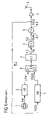
- FIG. 5 is a block diagram illustrating one possible embodiment of the circuit arrangement according to the invention for phase control.
- FIGS. 1 to 4 will not be described any further in the following text, since this has already been done above. Reference should be made to the above, for the explanation of the figures.
- the basic design of the circuit arrangement according to the invention for phase control as illustrated in FIG. 5 has a phase locked loop which corresponds in some respects to the phase locked loop shown in FIG. 1 .
- the phase locked loop is a component of the circuit arrangement according to the invention for phase control, with the invention not being restricted to the use of the phase locked loop shown in FIG. 1 .
- any phase locked loop is in principle suitable for this purpose.
- the phase detector 3 ′ that is shown in FIG. 5 has an additional control input 3 . 4 , which is connected to a control output 54 . 3 of a control unit 54 .
- the charge pump 4 ′ in FIG. 5 differs from the charge pump 4 shown in FIG. 1 in that the charge pump 4 ′ has an additional control input 4 . 3 , which is connected to the output 53 . 3 of a computation unit 53 .
- the output 6 . 2 of the voltage controlled oscillator 6 in FIG. 5 is additionally connected to a measurement input 51 . 1 of a frequency meter 51 , which is used to detect the frequency FVCO that is produced by the voltage controlled oscillator 6 .
- the frequency meter 51 receives, via its control input 51 . 2 , the appropriate control command from the control unit 54 via its control output 54 . 1 , the frequency FVCO is detected, and is passed via the output 51 . 3 of the frequency meter 51 to a memory 52 .
- the memory 52 is controlled via the control input 52 . 2 , which is connected to the control output 54 . 2 of the control unit 54 .
- the control unit 54 has transmitted the appropriate control command to the memory 52 , the value for the frequency FVCO that is stored in the memory 52 is transmitted to the computation unit 53 , via its input 53 . 1 .
- the gradient KVCO of the voltage controlled oscillator 6 is calculated.
- a correction value K which is obtained from this is passed via the output 53 . 3 of the computation unit 53 to the charge pump 4 ′.
- the effective gradient KVCO of the voltage controlled oscillator 6 that actually occurs during operation is determined, and is then adjusted, by means of the circuit arrangement according to the invention for phase control.
- the adjustment or correction is based on the gradient KVCO.
- the correction is carried out via the charge pump current Icp of the charge pump 4 ′ in the phase locked loop PLL.
- the loop gain of the phase locked loop is thus influenced.
- the product of the gradient KVCO and of the charge pump current Icp (KVCO*Icp) and thus the loop bandwidth ⁇ x are set and regulated to the desired or required value by means of the correction value K.
- a synchronous or asynchronous divider of counter can be used, for example, as the frequency meter 51 , which is also referred to as a frequency-processing unit.
- the computation unit 53 uses only two frequencies for calculation of the correction value K, then it is sufficient for the memory 52 to have two digital registers, for example a register A for the first frequency, and a register B for the second frequency.
- the control unit 54 sets all of the connected units, that is to say the frequency meter 51 , the memory 52 , the phase detector 3 ′ and the computation unit 53 , to a basic state. Via the control output 54 . 3 , the control unit 54 then sets the phase detector 3 ′ to a mode in which the phase detector 3 ′ produces a first, fixed duty cycle PW 1 .
- the control unit 54 causes the frequency meter 51 to carry out a frequency measurement and to pass the result, for example as a count cnt 1 , to the register A of the memory 52 .
- control unit 54 then causes the frequency meter 51 once again to carry out a further frequency measurement, and to transfer the measurement value cnt 2 to the register B of the memory unit 52 . Finally, the control unit 54 causes the computation unit 53 to calculate the gradient using the two measurement values cnt 1 and cnt 2 , and to pass the corresponding correction value K to the charge pump 4 ′.
- the frequency counter 51 is activated for a specific time period, for example for 128/26 ⁇ s.
- the computation unit 53 uses this to produce the correction for the charge pump current Icp, by reducing it by 20.27%.
- the product KVCO*Icp is constant, and the loop bandwidth ⁇ x of the system is thus set to the desired value.
- CFT[ 5 . . . 0] (( DCNT — NOM[ 9 . . . 0 ] SHL 2)/ DCNT — MEAS[ 12 . . . 0]) ⁇ CFT — OFF (4 . . . 0)
- SHL 2 is a correction factor (*4) for calculation of the charge pump manipulated variable.
- DCNT_MEAS is a 13 bit word and represents the difference between the two measured frequencies cnt 1 and cnt 2 . The units are pulses per period.
- the result CFT which is annotated with K in FIG. 5 , is a 6 bit word. This controls a digital/analog converter, which is provided directly in the charge pump 4 .
- the main components of the computation unit 53 are a divider and a subtractor.
- the necessary correction factor K is calculated as already described, is weighted and is used for linear variation of the duty cycle in the phase detector 3 ′.
- This may be implemented using a digital/analog converter, for example by conversion of the correction word K to an analog delay, or completely digitally, for example by multiplexing delay chains or by the use of a programmable counter at a higher frequency.
- the computation unit 53 can also pass the correction value K to the loop filter 5 . This is done, for example, by a digital/analog converter converting the correction word K to a programmable resistance.
- the effective transfer function that is to say the loop bandwidth ⁇ x of the phase locked loop as well, can thus be adapted for the measured gradient of the voltage controlled oscillator.
- the collection value K can be passed directly from the computation unit 53 to the voltage controlled oscillator 6 .
- varactors in the voltage controlled oscillator core can be connected or disconnected in accordance with the calculated correction value, for control purposes.
Landscapes
- Stabilization Of Oscillater, Synchronisation, Frequency Synthesizers (AREA)
- Inverter Devices (AREA)
Abstract
Description
where
- ZF(s)=the transfer function of the loop filter,
- KVCO=the gradient of the voltage controlled oscillator,
- Icp=the charge pump current
- C1=a first capacitance of the loop filter,
- R1=a first resistance of the loop filter, and
- C2=a second capacitance of the loop filter.
- OpenLoopGain=f(KVCO, Icp, LF(Cx, Rx)),
where LF(Cx, Rx) represents the characteristics of the loop filter as a function of the capacitances Cx and of the resistances Rx.
- Charge pump current Icp(Kphi)=1 mA on 1 kOhm
- Frequency of the voltage controlled oscillator: FVCO=˜3000 MHz . . . 4000 MHz
| TABLE 1 |
| ideal case: |
| Gradient KVCO = 60 MHz/V |
| Calculation of the nominal values: |
| Unit | T1a + b | T2a + b | |
| Duty | PW1 | 1:4 | PW2 | 2:3 | |
| cycle | |||||
| Voltage | => | Vtune1 | 0.2 | Vtune2 | 0.4 |
| Frequency | => | FVCO1 | 3.500 E9 | FVCO2 | 3.512 E9 |
| Count | => | cnt_nom1 | 17230.77 | cnt-nom2 | 17289.85 |
| after | |||||
| 128/26 μs | |||||
| Delta | => | delta_cnt_nom | 59 | ||
where:
- cnt_nom1=first nominal count, corresponding to the measured first frequency,
- cnt_nom2=second nominal count, corresponding to the measured second frequency,
- delta_cnt_nom=nominal difference between cnt_nom_1 and cnt_nom_2.
| TABLE 2 |
| actual case: |
| The gradient KVCO is calculated to be: |
| KVCO = 75 MHz/V − (FVCO2 − FVCO1)/(Vtune2 − Vtune1) |
| Unit | T1a + b | T2a + b | |
| Duty | PW1 | 1:4 | PW2 | 2:3 | |
| cycle | |||||
| Voltage | => | Vtune1 | 0.2 | Vtune2 | 0.4 |
| Frequency | => | FVCO1 | 3.484530 | FVCO2 | 3.499630 |
| E9 | E9 | ||||
| Count | => | cnt1 | 17154.61 | cnt2 | 17228.95 |
| after | (mea- | (measured) | |||
| 128/26 μs | sured) | ||||
| Delta | => | del- | 74.3 | ||
| ta_cnt | |||||
K=KVCO — aim/KVCO — real=delta — cnt — nom/delta — cnt=delta — cnt — nom/(cnt2−cnt1)=0.797
CFT[5 . . . 0]=((DCNT — NOM[9 . . . 0] SHL2)/DCNT — MEAS[12 . . . 0])−CFT — OFF(4 . . . 0)
- 1 Reference oscillator
- 2 1/R divider
- 3, 3′ Phase detector
- 3.1 First input of the phase detector
- 3.2 Second input of the phase detector
- 3.3 Output of the phase detector
- 3.4 Control input
- 4, 4′ Charge pump
- 4.1 Input of the charge pump
- 4.2 Output of the charge pump
- 4.3 Control input
- 5 Loop filter
- 5.1 Input of the loop filter
- 5.2 Output of the loop filter
- 6 Voltage controlled oscillator
- 6.1 VCO input
- 6.2 VCO output
- 7 1/N divider
- 8 Power amplifier
- 9 Antenna
- 25 Subtraction unit
- 21, 22, 23 Control path
- 24 Feedback path with a 1/N divider
- 31, 32 Sections of the transfer function
- 41, 42 Transfer functions of the filter
- 51 Frequency meter
- 51.2 Control input
- 52 Memory
- 5.2 Control input
- 53 Computation unit
- 53.2 Control input of the computation unit
- 54 Control unit
- 54.1–54.4 Control outputs
- FVCO Frequency of the VCO
- FVCO′ Divided frequency of the VCO
- Fref Reference frequency
- Fref′ Divided reference frequency
- PLL Phase locked loop
- K Correction value
- Vtune Tuning voltage
- Icp Charge pump current
Claims (18)
Applications Claiming Priority (3)
| Application Number | Priority Date | Filing Date | Title |
|---|---|---|---|
| DEDE10255145.6 | 2002-11-26 | ||
| DE10255145A DE10255145B4 (en) | 2002-11-26 | 2002-11-26 | Circuit arrangement for phase control and method for operating the circuit arrangement |
| PCT/DE2003/003537 WO2004049573A2 (en) | 2002-11-26 | 2003-10-24 | Phase-control circuit arrangement and method for operating said circuit arrangement |
Related Parent Applications (1)
| Application Number | Title | Priority Date | Filing Date |
|---|---|---|---|
| PCT/DE2003/003537 Continuation WO2004049573A2 (en) | 2002-11-26 | 2003-10-24 | Phase-control circuit arrangement and method for operating said circuit arrangement |
Publications (2)
| Publication Number | Publication Date |
|---|---|
| US20050264368A1 US20050264368A1 (en) | 2005-12-01 |
| US7068112B2 true US7068112B2 (en) | 2006-06-27 |
Family
ID=32318695
Family Applications (1)
| Application Number | Title | Priority Date | Filing Date |
|---|---|---|---|
| US11/136,232 Expired - Fee Related US7068112B2 (en) | 2002-11-26 | 2005-05-24 | Phase-control circuit arrangement and method for operating said circuit arrangement |
Country Status (4)
| Country | Link |
|---|---|
| US (1) | US7068112B2 (en) |
| AU (1) | AU2003286108A1 (en) |
| DE (1) | DE10255145B4 (en) |
| WO (1) | WO2004049573A2 (en) |
Cited By (6)
| Publication number | Priority date | Publication date | Assignee | Title |
|---|---|---|---|---|
| US7382201B1 (en) | 2007-03-23 | 2008-06-03 | Mediatek Inc. | Signal generating apparatus and method thereof |
| US20080232443A1 (en) * | 2007-03-23 | 2008-09-25 | Tai-Yuan Yu | Signal generating apparatus |
| US20080272811A1 (en) * | 2007-03-23 | 2008-11-06 | Hsin-Hung Chen | Signal generating apparatus and method thereof |
| US20090072911A1 (en) * | 2007-09-14 | 2009-03-19 | Ling-Wei Ke | Signal generating apparatus and method thereof |
| US20090322439A1 (en) * | 2008-06-26 | 2009-12-31 | Infineon Technologies Ag | Phase locked loop based frequency modulator with accurate oscillator gain adjustment |
| US20100183091A1 (en) * | 2009-01-22 | 2010-07-22 | Chi-Hsueh Wang | Method for tuning a digital compensation filter within a transmitter, and associated digital compensation filter and associated calibration circuit |
Families Citing this family (2)
| Publication number | Priority date | Publication date | Assignee | Title |
|---|---|---|---|---|
| DE10308643A1 (en) | 2003-02-27 | 2004-09-16 | Infineon Technologies Ag | Phase regulating arrangement |
| US8154356B2 (en) | 2009-12-19 | 2012-04-10 | Infineon Technologies Ag | Oscillator with capacitance array |
Citations (8)
| Publication number | Priority date | Publication date | Assignee | Title |
|---|---|---|---|---|
| US4105948A (en) | 1977-04-18 | 1978-08-08 | Rca Corporation | Frequency synthesizer with rapidly changeable frequency |
| US4743867A (en) * | 1987-08-03 | 1988-05-10 | Motorola, Inc. | Compensation circuitry for dual port phase-locked loops |
| US4926141A (en) | 1989-05-01 | 1990-05-15 | Motorola, Inc. | Frequency synthesizer with improved automatic control of loop bandwidth selection |
| US5625325A (en) | 1995-12-22 | 1997-04-29 | Microtune, Inc. | System and method for phase lock loop gain stabilization |
| US5631587A (en) | 1994-05-03 | 1997-05-20 | Pericom Semiconductor Corporation | Frequency synthesizer with adaptive loop bandwidth |
| US5648744A (en) | 1995-12-22 | 1997-07-15 | Microtune, Inc. | System and method for voltage controlled oscillator automatic band selection |
| US5786733A (en) | 1995-12-04 | 1998-07-28 | Nec Corporation | Phase-locked oscillating circuit with a frequency fluctuation detecting circuit |
| DE10125373A1 (en) | 2001-05-23 | 2002-12-05 | Infineon Technologies Ag | Phase-locked loop |
-
2002
- 2002-11-26 DE DE10255145A patent/DE10255145B4/en not_active Expired - Fee Related
-
2003
- 2003-10-24 WO PCT/DE2003/003537 patent/WO2004049573A2/en not_active Ceased
- 2003-10-24 AU AU2003286108A patent/AU2003286108A1/en not_active Abandoned
-
2005
- 2005-05-24 US US11/136,232 patent/US7068112B2/en not_active Expired - Fee Related
Patent Citations (8)
| Publication number | Priority date | Publication date | Assignee | Title |
|---|---|---|---|---|
| US4105948A (en) | 1977-04-18 | 1978-08-08 | Rca Corporation | Frequency synthesizer with rapidly changeable frequency |
| US4743867A (en) * | 1987-08-03 | 1988-05-10 | Motorola, Inc. | Compensation circuitry for dual port phase-locked loops |
| US4926141A (en) | 1989-05-01 | 1990-05-15 | Motorola, Inc. | Frequency synthesizer with improved automatic control of loop bandwidth selection |
| US5631587A (en) | 1994-05-03 | 1997-05-20 | Pericom Semiconductor Corporation | Frequency synthesizer with adaptive loop bandwidth |
| US5786733A (en) | 1995-12-04 | 1998-07-28 | Nec Corporation | Phase-locked oscillating circuit with a frequency fluctuation detecting circuit |
| US5625325A (en) | 1995-12-22 | 1997-04-29 | Microtune, Inc. | System and method for phase lock loop gain stabilization |
| US5648744A (en) | 1995-12-22 | 1997-07-15 | Microtune, Inc. | System and method for voltage controlled oscillator automatic band selection |
| DE10125373A1 (en) | 2001-05-23 | 2002-12-05 | Infineon Technologies Ag | Phase-locked loop |
Non-Patent Citations (1)
| Title |
|---|
| International Search Report for Int'l Application No. PCT/DE03/03537, Int'l Filing Date Oct. 24, 2003, 2 pgs. |
Cited By (10)
| Publication number | Priority date | Publication date | Assignee | Title |
|---|---|---|---|---|
| US7382201B1 (en) | 2007-03-23 | 2008-06-03 | Mediatek Inc. | Signal generating apparatus and method thereof |
| US20080232443A1 (en) * | 2007-03-23 | 2008-09-25 | Tai-Yuan Yu | Signal generating apparatus |
| US20080272811A1 (en) * | 2007-03-23 | 2008-11-06 | Hsin-Hung Chen | Signal generating apparatus and method thereof |
| US7486118B2 (en) | 2007-03-23 | 2009-02-03 | Mediatek Inc. | Signal generating apparatus and method thereof |
| US20090072911A1 (en) * | 2007-09-14 | 2009-03-19 | Ling-Wei Ke | Signal generating apparatus and method thereof |
| US20090322439A1 (en) * | 2008-06-26 | 2009-12-31 | Infineon Technologies Ag | Phase locked loop based frequency modulator with accurate oscillator gain adjustment |
| US7760042B2 (en) | 2008-06-26 | 2010-07-20 | Infineon Technologies Ag | Phase locked loop based frequency modulator with accurate oscillator gain adjustment |
| US20100183091A1 (en) * | 2009-01-22 | 2010-07-22 | Chi-Hsueh Wang | Method for tuning a digital compensation filter within a transmitter, and associated digital compensation filter and associated calibration circuit |
| US8081936B2 (en) | 2009-01-22 | 2011-12-20 | Mediatek Inc. | Method for tuning a digital compensation filter within a transmitter, and associated digital compensation filter and associated calibration circuit |
| US8892060B2 (en) | 2009-01-22 | 2014-11-18 | Mediatek Inc. | Method for tuning a digital compensation filter within a transmitter, and associated digital compensation filter |
Also Published As
| Publication number | Publication date |
|---|---|
| DE10255145B4 (en) | 2005-12-29 |
| AU2003286108A8 (en) | 2004-06-18 |
| WO2004049573A3 (en) | 2004-08-05 |
| WO2004049573A2 (en) | 2004-06-10 |
| DE10255145A1 (en) | 2004-06-17 |
| AU2003286108A1 (en) | 2004-06-18 |
| US20050264368A1 (en) | 2005-12-01 |
Similar Documents
| Publication | Publication Date | Title |
|---|---|---|
| CN107026646B (en) | Digital phase-locked loop | |
| KR100682279B1 (en) | Adaptive frequency regulator of frequency synthesizer | |
| US7982552B2 (en) | Automatic frequency calibration apparatus and method for a phase-locked loop based frequency synthesizer | |
| US10263626B2 (en) | Apparatus and methods for tuning a voltage controlled oscillator | |
| US8896386B2 (en) | Calibration device for oscillator and method thereof | |
| JP2000509219A (en) | Frequency synthesizer having temperature compensation and frequency multiplication functions and method of manufacturing the same | |
| US9515669B2 (en) | Hybrid phase locked loop having wide locking range | |
| US20040109521A1 (en) | Phase locked loop frequency synthesizer where frequency gain variation controlled oscillator is compensated | |
| US7292119B2 (en) | Phase locked loop frequency synthesizer | |
| US7154342B2 (en) | Phase locked loop circuit with a tunable oscillator and an independent frequency converter and frequency counter | |
| CN1813407B (en) | Method and device for automatically calibrating a loop-filter of a phase locked loop | |
| US7068112B2 (en) | Phase-control circuit arrangement and method for operating said circuit arrangement | |
| EP1988634B1 (en) | Pll circuit | |
| US7772930B2 (en) | Calibration techniques for phase-locked loop bandwidth | |
| US7821345B2 (en) | Calibrating an oscillator and corresponding calibration device | |
| US7106141B2 (en) | Phase locked loop | |
| US20030216130A1 (en) | Phase locking loop frequency synthesiser | |
| EP1226452B1 (en) | Radio calibration by correcting the crystal oscillator frequency | |
| KR102173075B1 (en) | Frequency synthesizer based on artificial intelligence and automatic compensation circuit therefor | |
| EP4525309A1 (en) | Phase-locked loop circuit and corresponding method of operation | |
| EP1638207B1 (en) | Method of calibrating the frequency of an oscillator in a phase locked loop circuit | |
| CN121036755A (en) | A Low-Noise Dual-Path Digital Auxiliary Phase-Locked Loop Circuit for Large-Area Image Sensors | |
| KR20080024896A (en) | Gain measurement method of voltage controlled oscillator and frequency synthesizer using same | |
| JP2005260598A (en) | Method for manufacturing PLL control signal generator | |
| HK1091964B (en) | A method and device for automatically calibrating a loop-filter of a phase locked loop |
Legal Events
| Date | Code | Title | Description |
|---|---|---|---|
| AS | Assignment |
Owner name: INFINEON TECHNOLOGIES AG, GERMANY Free format text: ASSIGNMENT OF ASSIGNORS INTEREST;ASSIGNORS:GOTZ, EDMUND;MARZINGER, GUNTER;SCHOLZ, MARKUS;AND OTHERS;REEL/FRAME:016884/0801;SIGNING DATES FROM 20050617 TO 20050712 |
|
| FPAY | Fee payment |
Year of fee payment: 4 |
|
| AS | Assignment |
Owner name: INFINEON TECHNOLOGIES DELTA GMBH, GERMANY Free format text: ASSIGNMENT OF ASSIGNORS INTEREST;ASSIGNOR:INFINEON TECHNOLOGIES AG;REEL/FRAME:026685/0688 Effective date: 19990930 |
|
| AS | Assignment |
Owner name: INFINEON TECHNOLOGIES DELTA GMBH, GERMANY Free format text: CORRECTIVE ASSIGNMENT TO CORRECT THE EFFECTIVE DATE NEEDS TO BE CORRECT TO 09/30/2009 PREVIOUSLY RECORDED ON REEL 026685 FRAME 0688. ASSIGNOR(S) HEREBY CONFIRMS THE ASSIGNMENT;ASSIGNOR:INFINEON TECHNOLOGIES AG;REEL/FRAME:027245/0484 Effective date: 20090930 |
|
| AS | Assignment |
Owner name: INTEL MOBILE COMMUNICATIONS TECHNOLOGY GMBH, GERMA Free format text: ASSIGNMENT OF ASSIGNORS INTEREST;ASSIGNOR:INFINEON TECHNOLOGIES DELTA GMBH;REEL/FRAME:027531/0108 Effective date: 20110131 |
|
| AS | Assignment |
Owner name: INTEL MOBILE COMMUNICATIONS GMBH, GERMANY Free format text: ASSIGNMENT OF ASSIGNORS INTEREST;ASSIGNOR:INTEL MOBILE COMMUNICATIONS TECHNOLOGY GMBH;REEL/FRAME:027556/0709 Effective date: 20111031 |
|
| FPAY | Fee payment |
Year of fee payment: 8 |
|
| AS | Assignment |
Owner name: INTEL DEUTSCHLAND GMBH, GERMANY Free format text: CHANGE OF NAME;ASSIGNOR:INTEL MOBILE COMMUNICATIONS GMBH;REEL/FRAME:037057/0061 Effective date: 20150507 |
|
| FEPP | Fee payment procedure |
Free format text: MAINTENANCE FEE REMINDER MAILED (ORIGINAL EVENT CODE: REM.) |
|
| LAPS | Lapse for failure to pay maintenance fees |
Free format text: PATENT EXPIRED FOR FAILURE TO PAY MAINTENANCE FEES (ORIGINAL EVENT CODE: EXP.) |
|
| STCH | Information on status: patent discontinuation |
Free format text: PATENT EXPIRED DUE TO NONPAYMENT OF MAINTENANCE FEES UNDER 37 CFR 1.362 |
|
| FP | Lapsed due to failure to pay maintenance fee |
Effective date: 20180627 |
|
| AS | Assignment |
Owner name: INTEL CORPORATION, CALIFORNIA Free format text: ASSIGNMENT OF ASSIGNORS INTEREST;ASSIGNOR:INTEL DEUTSCHLAND GMBH;REEL/FRAME:061356/0001 Effective date: 20220708 |