US7064699B2 - Current cell matrix type digital-to-analog converter - Google Patents
Current cell matrix type digital-to-analog converter Download PDFInfo
- Publication number
- US7064699B2 US7064699B2 US10/983,644 US98364404A US7064699B2 US 7064699 B2 US7064699 B2 US 7064699B2 US 98364404 A US98364404 A US 98364404A US 7064699 B2 US7064699 B2 US 7064699B2
- Authority
- US
- United States
- Prior art keywords
- current
- offset
- matrix type
- signal
- cell matrix
- Prior art date
- Legal status (The legal status is an assumption and is not a legal conclusion. Google has not performed a legal analysis and makes no representation as to the accuracy of the status listed.)
- Expired - Lifetime, expires
Links
Images


Classifications
-
- H—ELECTRICITY
- H03—ELECTRONIC CIRCUITRY
- H03M—CODING; DECODING; CODE CONVERSION IN GENERAL
- H03M1/00—Analogue/digital conversion; Digital/analogue conversion
- H03M1/06—Continuously compensating for, or preventing, undesired influence of physical parameters
- H03M1/0602—Continuously compensating for, or preventing, undesired influence of physical parameters of deviations from the desired transfer characteristic
- H03M1/0604—Continuously compensating for, or preventing, undesired influence of physical parameters of deviations from the desired transfer characteristic at one point, i.e. by adjusting a single reference value, e.g. bias or gain error
- H03M1/0607—Offset or drift compensation
-
- H—ELECTRICITY
- H03—ELECTRONIC CIRCUITRY
- H03M—CODING; DECODING; CODE CONVERSION IN GENERAL
- H03M1/00—Analogue/digital conversion; Digital/analogue conversion
- H03M1/66—Digital/analogue converters
- H03M1/68—Digital/analogue converters with conversions of different sensitivity, i.e. one conversion relating to the more significant digital bits and another conversion to the less significant bits
- H03M1/682—Digital/analogue converters with conversions of different sensitivity, i.e. one conversion relating to the more significant digital bits and another conversion to the less significant bits both converters being of the unary decoded type
- H03M1/685—Digital/analogue converters with conversions of different sensitivity, i.e. one conversion relating to the more significant digital bits and another conversion to the less significant bits both converters being of the unary decoded type the quantisation value generators of both converters being arranged in a common two-dimensional array
-
- H—ELECTRICITY
- H03—ELECTRONIC CIRCUITRY
- H03M—CODING; DECODING; CODE CONVERSION IN GENERAL
- H03M1/00—Analogue/digital conversion; Digital/analogue conversion
- H03M1/66—Digital/analogue converters
- H03M1/68—Digital/analogue converters with conversions of different sensitivity, i.e. one conversion relating to the more significant digital bits and another conversion to the less significant bits
- H03M1/687—Segmented, i.e. the more significant bit converter being of the unary decoded type and the less significant bit converter being of the binary weighted type
-
- H—ELECTRICITY
- H03—ELECTRONIC CIRCUITRY
- H03M—CODING; DECODING; CODE CONVERSION IN GENERAL
- H03M1/00—Analogue/digital conversion; Digital/analogue conversion
- H03M1/66—Digital/analogue converters
- H03M1/74—Simultaneous conversion
- H03M1/742—Simultaneous conversion using current sources as quantisation value generators
- H03M1/745—Simultaneous conversion using current sources as quantisation value generators with weighted currents
-
- H—ELECTRICITY
- H03—ELECTRONIC CIRCUITRY
- H03M—CODING; DECODING; CODE CONVERSION IN GENERAL
- H03M1/00—Analogue/digital conversion; Digital/analogue conversion
- H03M1/66—Digital/analogue converters
- H03M1/74—Simultaneous conversion
- H03M1/742—Simultaneous conversion using current sources as quantisation value generators
- H03M1/747—Simultaneous conversion using current sources as quantisation value generators with equal currents which are switched by unary decoded digital signals
Definitions
- the present invention relates to a current-cell matrix type digital-to-analog converter for producing an analog signal output corresponding to a digital signal input thereto.
- D/A converter when some current matrix type digital-to-analog (D/A) converter receives an analog output from a circuit, LSI (Large Scale Integration), or the like having an offset voltage, for example, directly connected thereto without a capacitor, the D/A converter applies the analog output with an offset voltage in conformity to the offset voltage of the connected circuit for adjustment.
- LSI Large Scale Integration
- a digital communication transmitter or the like comprises a modulator 1 for generating a baseband signal; and an orthogonal modulator 2 for orthogonally modulating the baseband signal in an analog domain to output an orthogonal modulated signal.
- the modulator 1 and the orthogonal modulator 2 are composed of semiconductor integrated circuits manufactured through different processes, they can differ from each other in signal potentials which maximize the performance, such as a signal-to-noise ratio, a modulation accuracy, and the like.
- baseband signals I(t) and Q(t) from the modulator 1 must be applied with offset voltages, respectively, for adjustment such that a DC level signal potential of the baseband signals I(t) and Q(t), i.e., the signal ground potential matches a signal ground potential which is optimal for the performance of the orthogonal modulator 2 .
- the modulator 1 applies serial-to-parallel conversion on a binary transmission data in a logic circuit 3 , and further differentially encodes the resulting parallel binary transmission data which is output to signal waveform generators 4 , 5 that output baseband signals I(t) and Q(t) to the orthogonal modulator 2 , respectively.
- the signal waveform generator 4 inputs a digital signal from a ROM (Read Only Memory) 6 to a current-cell matrix type D/A converter 910 for processing.
- the resulting analog signal is applied with an offset voltage in a level shifter circuit 920 to generate a baseband signal which is output through a low pass filter 7
- the current-cell matrix type D/A converter 910 described in Japanese Patent Application Kokai No. 9-51360 (hereinafter referred to as “patent document-1”) is connected to a level shift circuit 920 , and outputs an analog signal Vout to the level shift circuit 920 , as shown in FIG. 12 .
- the level shift circuit 920 has a first signal level shifter 930 which adds a level shift voltage to the analog signal Vout to output a baseband signal Vls to which an offset voltage has been applied.
- the level shift circuit 920 comprises a first level shifter 930 ; a signal ground potential determination circuit 940 which is a first reference potential generating means; a signal center potential reference circuit 950 which is a second reference potential generating means; a second signal level shifter 960 ; and an operational amplifier 970 .
- the current-cell matrix type D/A converter 910 comprises a row decoder 12 , a column decoder 14 , a load resistor 24 , and a plurality of unit current cells 912 , 914 , 916 , 918 .
- the level shift circuit 920 selects a unit current cell in accordance with a 10-bit input code 102 , and applies the load resistor 24 with a current flowing from the selected unit current cell to determine the potential for the analog signal Vout.
- a plurality of unit current cells 912 , 914 , 916 , 918 are each configured as shown in FIG. 13 .
- each of the unit current cells 912 outputs a predetermined output when a row decode signal and a column decode signal are both at “H.” This current value can be set by adjusting the width of a gate of a current regulating transistor 36 .
- each of the unit current cells is supplied with a bias voltage 104 input to the current-cell matrix type D/A converter 910 from the outside.
- the current-cell matrix type D/A converter 910 includes (2 6 -1) current cells 912 , having a current value of I0/2 7 , arranged on an array, and one each of the unit current cell 914 having a current value of I0/2 8 , the unit current cell 916 having a current value of I0/2 9 , and the unit current cell 918 having a current value of I0/2 10 .
- the upper six bits of the input code 102 is D/A converted by a selected number of the unit current cells 912 having a current value of I0/2 7 , while the lower three bits of the input code 102 are D/A converted depending on whether to select the unit current cells 914 , 916 , 918 , the current values of which are weighted, resulting in 9-bit D/A conversion in total.
- the first signal level shifter 930 which comprises a source follower circuit made up of PMOS (P-channel Metal-Oxide Semiconductor) transistors 932 , 934 , adds a level shift voltage to the analog signal Vout output from the current-cell matrix type D/A converter 910 in an analog domain to output the baseband signal Vls.
- PMOS P-channel Metal-Oxide Semiconductor
- the PMOS 932 is applied with the analog signal Vout at its gate
- the PMOS 934 is applied with an output potential Vbls from the operational amplifier 970 at its gate to output the signal Vls from the source of the PMOS 932 (drain of the PMOS 934 ).
- the signal ground potential determination circuit 940 is comprised of a plurality of resistors 942 connected in series between a power supply and the ground, and a selector circuit 944 .
- the selector circuit 944 selects a potential at one connection from the plurality of resistors 942 in accordance with an offset voltage adjusting signal 980 input thereto to determine a signal ground voltage Vsg as a first reference potential.
- the signal center potential reference circuit 950 which is comprised of resistors 952 , 954 connected in series between the power supply and ground, outputs the potential at a connection of the two resistors as a signal center potential Vm which is a second reference potential.
- the resistances of the resistors 952 , 954 are set such that the potential Vm is equal to a center potential Vct of the analog voltage Vout output from the current-cell matrix type D/A converter 910 .
- the second signal level shifter 960 is identical in configuration to the first signal level shifter 930 , or is designed such that a device size ratio of a PMOS transistor 962 to a PMOS transistor 964 is equal to a device size ratio of the PMOS 932 to PMOS 934 , with the PMOSs 932 , 934 making up the first signal level shifter 930 .
- the PMOS 962 is applied at its gate with the signal center potential Vm from the signal center potential reference circuit 950
- the PMOS 964 is applied at its gate with the bias potential signal Vbls from the operational amplifier 970 , causing a potential Vrpl to be output from the source of the PMOS 964 (drain of the PMOS 964 ).
- each of the signal waveform generators 4 , 5 for supplying a baseband signal to the orthogonal modulator 2 comprises the current-cell matrix type D/A converter 910 as described above, and can adjust an the offset signal applied to the baseband signal in order to match the signal ground potential for the baseband signal with an optimal signal ground potential for the performance of the orthogonal modulator 2 .
- the current-cell matrix type D/A converter described in the patent document-1 which is connected to a level shift circuit, can apply and adjust the offset voltage to the analog signal.
- the first signal level shifter When the analog signal output form the current-cell matrix type D/A converter is converted to a voltage by the level shift circuit to output the baseband signal, the first signal level shifter, in particular, is affected by the voltage-current (V-I) characteristic in the transistor 12 a to degrade the linearity of the output baseband signal.
- V-I voltage-current
- the present invention provides a current-cell matrix type digital-to-analog converter which includes a plurality of unit current cells arranged in a matrix form, each of which is selected or non-selected in accordance with a digital signal, a first connection line supplied with a first current from all selected unit current cells of the plurality of unit current cells, and a first load resistor connected to the first connection line and supplied with the first current, wherein the converter further includes a second connection line supplied with a second current which is an inverted output of the first current from all non-selected unit current cells of the plurality of unit current cells, and an offset adjuster circuit connected to the first connection line through a first load resistor and connected to the second connection line, the offset adjuster circuit produces a constant voltage based on the first current supplied from the first connection line and a second current supplied from the second connection line irrespective of whether the plurality of unit current cells are selected or non-selected, to generate an offset voltage, and the converter outputs a first analog voltage signal based on
- the current-cell matrix type D/A converter of the present invention by connecting currents from selected unit current cells and currents from non-selected unit current cells to the offset adjusting resister, a constant offset voltage can be generated irrespective of the selection of the unit current cells without increasing the circuit scale. Further, the offset voltage can be output without degrading the linearity thereof.
- the current-cell matrix type D/A converter includes a plurality of offset adjusting resistors, and switches associated with the plurality of offset adjusting resistors, respectively. By switching the switches in response to an offset voltage adjusting signal, the offset voltage can be adjusted.
- the current-cell matrix type D/A converter includes a load resistor supplied with currents from selected unit current cells, and a load resistor supplied with currents from non-selected unit current cells.
- the current-cell matrix type D/A converter can also generate the offset voltage even when a differential voltage is output, and can adjust the offset voltage value.
- FIG. 1 is a block diagram showing one embodiment of a current-cell matrix type D/A converter according to the present invention
- FIG. 2 is a block diagram illustrating a unit current cell in the current-cell matrix type D/A converter shown in FIG. 1 ;
- FIG. 3 is a diagram showing the waveform of an output voltage at the current-cell matrix type D/A converter shown in FIG. 1 ;
- FIG. 4 is a block diagram showing a digital communication transmitter
- FIG. 5 is a block diagram showing an exemplary circuit configuration of a current-cell matrix type D/A converter according to the present invention when it is applied to a signal waveform generator in the transmitter shown in FIG. 4 ;
- FIG. 6 is a block diagram showing another embodiment of the current-cell matrix type D/A converter according to the present invention.
- FIG. 7 is a block diagram showing another embodiment of the current-cell matrix type D/A converter according to the present invention.
- FIG. 8 is a diagram generally showing the waveform of an output voltage in the current-cell matrix type D/A converter shown in FIG. 5 ;
- FIG. 9 is a block diagram showing another embodiment of the current-cell matrix type D/A converter according to the present invention.
- FIG. 10 is a diagram generally showing the waveform of an output voltage in the current-cell matrix type D/A converter shown in FIG. 6 ;
- FIG. 11 is a diagram generally showing the waveform of an inverted output voltage in the current-cell matrix type D/A converter shown in FIG. 6 ;
- FIG. 12 is a diagram showing a conventional current-cell matrix type D/A converter
- FIG. 13 is a block diagram illustrating a unit current cell in the conventional current-cell matrix type D/A converter shown in FIG. 9 ;
- FIG. 14 is a block diagram showing an exemplary configuration of the conventional current-cell matrix type D/A converter when it is applied to the signal waveform generator in the transmitter shown in FIG. 4 .
- a current-cell matrix type D/A converter 10 is applied to a signal waveform generator 4 to process a digital signal from a ROM 6 , and output a baseband signal through a low pass filter 7 .
- a modulator 1 to which the signal waveform generator 4 is applied, applies serial-to-parallel conversion on binary transmission data in a logic circuit 3 , and further differentially encodes the resulting parallel signal which is output to signal wave generator circuits 4 , 5 , each including the current-cell matrix type D/A converter 10 .
- the signal waveform generators 4 , 5 output baseband signals I(t), Q(t), respectively, to an orthogonal modulator 2 .
- the modulator 1 and the orthogonal modulator 2 are composed of semiconductor integrated circuits manufactured through different processes, they can differ from each other in signal potentials which maximize the performance, such as a signal-to-noise ratio, a modulation accuracy, and the like.
- the D/A converter 10 to orthogonal modulator 2 in each of the signal waveform generator 4 , 5 are made up of analog circuits, baseband signal I(t) and Q(t) must be applied with offset voltages, respectively, for adjustment such that DC level signal potential of the baseband signals I(t) and Q(t), i.e., the signal ground potential matches a signal ground potential which is optimal for the performance of the orthogonal modulator 2 .
- an embodiment of the current-cell matrix type D/A converter 10 supplies an input code 102 , which is a digital signal, to a plurality of unit current cells 16 , 18 , 20 , 22 through a row decoder 12 and a column decoder 14 to select a desired unit current cell, supplies currents from the selected unit current cells to an offset adjuster circuit 26 through a load resistor 24 , and supplies currents from non-selected unit current cells to the offset adjuster circuit 26 to generate an offset voltage Vos, for outputting an analog voltage Vout. Illustration is omitted for parts not directly related to the present invention to avoid redundant description.
- the row decoder 12 and column decoder 14 supply a row decode signal and a column decode signal, respectively, in accordance with the input code 102 , to a plurality of unit current cells 16 , 18 , 20 , 22 to select desired unit current cells.
- each signal is identified by a reference numeral which designates a connection line on which the signal appears.
- a matrix is made up of the unit current cells 16 for D/A converting the upper six bits of the input code 102 ; and a plurality of unit current cells including the unit current cells 18 , 20 , 22 for D/A converting the lower three bits of the input code 102 .
- the (2 6 -1) unit current cells 16 are arranged in an array form on the matrix for converting the upper six bits.
- the unit current cells 18 , 20 , 22 are individually arranged for representing the lowerbits.
- the unit cells 18 , 20 , 22 are weighted by 1/2 1 , 1/2 2 , 1/2 3 , respectively, from the upper bit with respect to the unit current cells 16 .
- a selected unit current cell 16 outputs a current value of I0/2 7 to a connection line 108
- the selected unit current cells 18 , 20 , 22 output current values of I0/2 8 , I0/2 9 , I0/2 10 , respectively, to the output line.
- the current value I0 is a full scale current value when all output currents flow from a plurality of unit current cells into the load current 24 .
- Unit current cells, which are not selected output similar current values to those which are output when they are selected.
- the unit current cell 16 comprises a switch logic circuit 32 connected to a row decode signal input terminal 202 and to a column decode signal input terminal 204 , and current regulating transistors 34 , 36 , 38 , as shown in FIG. 2 .
- the unit current cell 16 processes signals supplied from the switch logic circuit 32 , a power supply 40 , and bias voltage input terminals 206 , 208 , and outputs the processed signals to an output terminal 210 or to an inverted output terminal 212 .
- the unit current cells 18 , 20 , 22 are also built in a similar manner to the unit current cell 16 .
- row decode signal terminal 202 and column decode signal terminal 204 are applied with a row decode signal supplied from the row decoder 12 and a column decode signal supplied from the column decoder 14 , respectively.
- the bias voltage input terminals 206 , 208 are supplied with a bias voltage applied to the current-cell matrix D/A converter 10 from the outside.
- the switch logic circuit 32 outputs in an inverter configuration, and the transistor 38 is applied at its gate with a threshold voltage of an inverter in the switch logic circuit 32 as a bias voltage.
- the transistor 38 turns on, while the transistor 34 turns off, causing a current generated by the transistor 36 to fully flow through the transistor 38 to the output terminal 210 .
- the transistor 38 turns off, while the transistor 34 turns on, causing a current generated by the transistor 36 to fully flow through the transistor 34 to the inverted output terminal 212 .
- the transistor 38 may be applied at its gate with an inverted version of the output of the switch logic circuit 32 .
- the unit current cells 16 , 18 , 20 , 22 each output a predetermined current from the output terminal 210 when both the row decode signal and column decode signal indicate the H level.
- both the row decode signal and column decode signal do not indicate the H level, for example, when the row decode signal is at L level and the column decode signal is also at L level, or when the row decode signal is at L level but the column decode signal is at H level, or when the row decode signal is at H level but the column decode signal is at L level
- the unit current cells 16 , 18 , 20 , 22 each output a predetermined voltage from the inverted output terminal 212 .
- CMOS N-channel Metal-Oxide Semiconductor
- bipolar transistors may be used instead of the MOS transistors.
- the current value output from the output terminal 210 or inverted output terminal 212 can be set in accordance with an adjustment made for the gate width of the transistor 36 .
- the offset adjuster circuit 26 is a circuit for generating an offset voltage, i.e., a reference voltage, and comprises an adjusting resistor 28 having the resistance value Ros, and a ground GND. Also, a current from a selected unit current cell is mixed with currents from non-selected unit current cells at a connection 106 to generate a sum current Ios which is supplied to the offset adjusting resistor 28 to generate an offset voltage Vos thereacross. Therefore, the potential at the connection 106 is equal to the offset voltage Vos.
- the offset adjusting resistor 28 may be connected from the outside, with its resistance value Ros adjusted to change the offset voltage.
- an input code 102 which is a 9-bit digital signal, is first input to the current-cell matrix type D/A converter 10 , and supplied to the row decoder 12 and column decoder 14 .
- the upper six bits of the input code 102 are supplied to a plurality of unit current cells 16 , while the lower three bits are supplied to the unit current cells 18 , 20 , 22 .
- each unit current cell whether or not the unit current cell is selected is determined in accordance with the input code 102 .
- a current from a selected unit current cell is supplied to the connection line 108 , while currents from unit current cells not selected are supplied to a connection line 110 .
- the current Idac is also supplied to the connection 106 .
- connection 106 the currents from all unit current cells not selected are supplied to the connection 106 through the connection line 110 .
- the value of the current supplied from the connection line 110 is always equal to an inverse of the current supplied from the connection 108 .
- the currents supplied to the connection 106 are indicated by the sum of the currents supplied from the connection line 108 and connection line 110 , i.e., the sum Ios of the currents output by all the selected unit current cells and all the non-selected unit current cells.
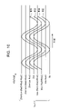
- the analog voltage Vout presents a waveform 304 which can be represented as shown in FIG. 3 , wherein a sinusoidal waveform 302 of the amplitude va, represented by the voltage Vac, indicates a zero scale (ZS), i.e., a reference potential.
- ZS zero scale
- the current-cell matrix type D/A converter 10 of the present invention may be applied with an n-bit (n is a natural number) digital signal as the input code 102 , a 9-bit digital signal is applied for avoiding the complexity in this embodiment. Also, while the unit current cells are arranged in a 9-bit matrix form in this embodiment, they may be arranged in an n-bit matrix form as long as equal currents flow through the respective rows.
- the current-cell matrix type D/A converter 10 comprises a capacitor 50 having a capacitance Cos in the offset adjuster circuit 26 , which has both ends connected to both ends of the offset adjusting resistor 28 , as shown in FIG.
- the predetermined current is supplied to the output terminal after the lapse of the off period, subsequent to the end of a supply to the inverted output terminal, when a transition is made from a state in which at least one of the row decode signal and column decode signal is at L level (i.e., when they are both at L level, or when one is at L level and the other is at H level, or when one is at H level and the other is at L level) to a state in which both the row decode signal and column decode signal are at H level (the respective signals are at H level and at H level, respectively).
- the predetermined current is supplied to the inverted output terminal after the lapse of the off period, subsequent to the end of a supply to the inverted output terminal, when a transition is made from the state in which both the row decode signal and column decode signal are at H level to the state in which at least one of the row decode signal and column decode signal is at L level.
- each current cell 16 is switched from selection to non-selection, a transient current flows through a parasitic capacitance of the transistor 36 , causing the current sum Ios to increase and decrease in the offset adjuster circuit 26 and the offset voltage Vos to fluctuate. As a result, the output voltage Vout is disturbed.
- the capacitor 50 in the current-cell matrix type D/A converter 10 of this embodiment absorbs fluctuations in the current sum Ios caused by the switching between selection and non-selection, thereby making it possible to suppress fluctuations in the offset voltage Vos to output a clear waveform of the output voltage Vout.
- a switch or the like may be associated with the capacitor in this embodiment to switch the fluctuation absorbing operation.
- the offset adjuster circuit 26 comprises an offset adjusting resistors 62 , 64 , 66 connected in series, a capacitor 50 , and switches 72 , 74 , 76 , as illustrated in FIG. 7 .
- the offset adjusting resistors 62 , 64 , 66 and switches 72 , 74 , 76 may be incorporated, for example, in an LSI, or implemented by an external circuit.
- the offset adjusting resistors 62 , 64 , 66 have resistance values Ros 1 , Ros 2 and Ros 3 , respectively, and are connected to the corresponding switches 72 , 74 , 76 , respectively.
- the switches 72 , 74 , 76 operates in accordance with offset voltage adjusting signals 502 , 504 , 506 , respectively.
- the switches turn on when the offset voltage adjusting signals are at H level to circumvent the corresponding offset adjusting resistors.
- PMOS transistors, NMOS transistors, or bipolar transistors are employed for the switches 72 , 74 , 76 in this embodiment.
- the output voltage Vout represents a waveform which shows that an offset signal is generated in accordance with the offset voltage adjusting signal, as shown in FIG. 8 .
- the switches 72 , 74 are turned on, while the switch 76 is turned off, and the adjusting resistors 62 , 64 are circumvented, but the adjusting resistor 66 is included in the current path, resulting in the offset voltage Vos calculated by Ros 3 ⁇ Ios.
- the output voltage Vout is output as indicated by a waveform 604 in FIG. 8 .
- the switch 72 When the adjusting signal 502 is at H level and the adjusting signals 504 , 506 are at L level, the switch 72 is turned on, while the switches 74 , 76 are turned off, and the adjusting resistor 62 is circumvented, but the adjusting resistors 64 , 66 are included in the current path, resulting in the offset voltage Vos calculated by (Ros 2 +Ros 3 ) ⁇ Ios.
- the output voltage Vout is output as indicated by a waveform 606 in FIG. 8 .
- the switches 72 , 74 , 76 are all turned off, and the adjusting resistors 62 , 64 , 66 are all included in the current path, resulting in the offset voltage Vos calculated by (Ros 1 +Ros 2 +Ros 2 ) ⁇ Ios.
- the output voltage Vout is output as indicated by a waveform 608 in FIG. 8 .
- FIG. 8 shows only a small number of offset adjusting resistors 62 , 64 , 66 for avoiding the complexity.
- the offset voltage adjuster circuit 26 may include a number of switches as much as the offset adjusting resistors, corresponding to the multiple offset adjusting resistors, wherein offset voltage adjusting signals are supplied corresponding to these switches.
- the current-cell matrix type D/A converter 10 supplies the load resistor 82 with the current Idac 1 from all selected unit current cells through the connection line 108 to output a voltage Vout 1 , and supplies the load current 84 with the current Idac 2 from all the non-selected unit current cell to output a voltage Vout 2 for differential output.
- the load resistors 82 , 84 have resistance values Rdac 1 , Rdac 2 , respectively, connected in parallel at a connection 702 , and are connected to the offset adjuster circuit 26 through the connection 702 .
- a current value supplied to the connection 702 i.e., the current value Ios supplied to the offset adjusting circuit 26 is calculated from the total sum of the current value Idac 1 supplied to the load resistor 82 and the current value Idac 2 supplied to the load resistor 84 .
- This current sum Ios is constant irrespective of which unit current cell is selected, as described above, and the current sum Ios is calculated by (I0/2 7 ⁇ (2 6 -1)+(I0/2 8 )+(10/2 9 )+(I0/2 10 ). Therefore, the current-cell matrix type D/A converter 10 of this embodiment can generate the offset voltage Vos without being affected by the load resistors 82 , 84 even if the voltage Vout 1 and voltage Vout 2 are differentially output.
- the current values Idac 1 , Idac 2 are such that their maximum value Ios and minimum value 0 are detected when all the unit current cells are selected, and the minimum value 0 and maximum value Ios are detected when non of the unit current cells is selected, thus having a relationship that Idac 2 decreases as Idac 1 increases with Ios at the maximum value, and Idac 2 increases as Idac 1 decreases.
- the current values Idac 1 , Idac 2 have a mutually reverse relationship.
- the output voltage Vout 1 from selected unit current cells is represented by waveforms 802 , 804 , 806 , 808 , in accordance with the offset voltage, as shown in FIG. 10 .
- the output voltage Vout 2 from non-selected unit current cells is represented by waveforms 812 , 814 , 816 , 818 , as shown in FIG. 11 .
- the shown waveforms are reverse to each other.
- the current-cell matrix type D/A converter 10 of this embodiment can generate an offset voltage and further adjust the offset voltage value even if differential voltages are output.
Landscapes
- Engineering & Computer Science (AREA)
- Theoretical Computer Science (AREA)
- Analogue/Digital Conversion (AREA)
Abstract
Description
Claims (7)
Applications Claiming Priority (2)
| Application Number | Priority Date | Filing Date | Title |
|---|---|---|---|
| JP2004-060412 | 2004-03-04 | ||
| JP2004060412A JP2005252663A (en) | 2004-03-04 | 2004-03-04 | Current cell matrix type digital/analog converter |
Publications (2)
| Publication Number | Publication Date |
|---|---|
| US20050200509A1 US20050200509A1 (en) | 2005-09-15 |
| US7064699B2 true US7064699B2 (en) | 2006-06-20 |
Family
ID=34918018
Family Applications (1)
| Application Number | Title | Priority Date | Filing Date |
|---|---|---|---|
| US10/983,644 Expired - Lifetime US7064699B2 (en) | 2004-03-04 | 2004-11-09 | Current cell matrix type digital-to-analog converter |
Country Status (2)
| Country | Link |
|---|---|
| US (1) | US7064699B2 (en) |
| JP (1) | JP2005252663A (en) |
Cited By (3)
| Publication number | Priority date | Publication date | Assignee | Title |
|---|---|---|---|---|
| US20070024479A1 (en) * | 2005-07-29 | 2007-02-01 | Tzu-Chao Lin | Digital-to-analog converter and related level shifter thereof |
| US9231546B2 (en) * | 2014-06-06 | 2016-01-05 | The Regents Of The University Of Michigan | Multi-dimensional array of impedance elements |
| US12439183B2 (en) | 2022-10-25 | 2025-10-07 | Samsung Electronics Co., Ltd. | Ramp signal generator for calibrating ramp linearity, operating method thereof, and image sensor device including the same |
Families Citing this family (5)
| Publication number | Priority date | Publication date | Assignee | Title |
|---|---|---|---|---|
| JP4799315B2 (en) * | 2006-08-10 | 2011-10-26 | パナソニック株式会社 | Digital to analog converter |
| JP2011259407A (en) * | 2010-05-13 | 2011-12-22 | Sony Corp | Signal processing circuit, solid state image sensor, and camera system |
| JP5959834B2 (en) * | 2011-12-02 | 2016-08-02 | キヤノン株式会社 | Imaging device |
| CN103905052B (en) * | 2012-12-28 | 2017-09-19 | 瑞昱半导体股份有限公司 | Method for setting current unit of current source |
| US10862500B1 (en) * | 2019-11-14 | 2020-12-08 | Xilinx, Inc. | Embedded variable output power (VOP) in a current steering digital-to-analog converter |
Citations (4)
| Publication number | Priority date | Publication date | Assignee | Title |
|---|---|---|---|---|
| JPH0951350A (en) | 1995-08-07 | 1997-02-18 | Nippon Telegr & Teleph Corp <Ntt> | Remote multiplex transmission device |
| US5760725A (en) * | 1995-03-29 | 1998-06-02 | Kawasaki Steel Corporation | Current cell type digital-analog converter |
| US5764094A (en) * | 1995-06-02 | 1998-06-09 | Matsushita Electric Industrial Co., Ltd. | Level shift circuit for analog signal and signal waveform generator including the same |
| US6353402B1 (en) * | 1999-11-08 | 2002-03-05 | Matsushita Electric Industrial Co., Ltd. | Current addition type D/A converter with low power consumption mode |
-
2004
- 2004-03-04 JP JP2004060412A patent/JP2005252663A/en active Pending
- 2004-11-09 US US10/983,644 patent/US7064699B2/en not_active Expired - Lifetime
Patent Citations (4)
| Publication number | Priority date | Publication date | Assignee | Title |
|---|---|---|---|---|
| US5760725A (en) * | 1995-03-29 | 1998-06-02 | Kawasaki Steel Corporation | Current cell type digital-analog converter |
| US5764094A (en) * | 1995-06-02 | 1998-06-09 | Matsushita Electric Industrial Co., Ltd. | Level shift circuit for analog signal and signal waveform generator including the same |
| JPH0951350A (en) | 1995-08-07 | 1997-02-18 | Nippon Telegr & Teleph Corp <Ntt> | Remote multiplex transmission device |
| US6353402B1 (en) * | 1999-11-08 | 2002-03-05 | Matsushita Electric Industrial Co., Ltd. | Current addition type D/A converter with low power consumption mode |
Cited By (4)
| Publication number | Priority date | Publication date | Assignee | Title |
|---|---|---|---|---|
| US20070024479A1 (en) * | 2005-07-29 | 2007-02-01 | Tzu-Chao Lin | Digital-to-analog converter and related level shifter thereof |
| US7199742B2 (en) * | 2005-07-29 | 2007-04-03 | United Microelectronics Corp. | Digital-to-analog converter and related level shifter thereof |
| US9231546B2 (en) * | 2014-06-06 | 2016-01-05 | The Regents Of The University Of Michigan | Multi-dimensional array of impedance elements |
| US12439183B2 (en) | 2022-10-25 | 2025-10-07 | Samsung Electronics Co., Ltd. | Ramp signal generator for calibrating ramp linearity, operating method thereof, and image sensor device including the same |
Also Published As
| Publication number | Publication date |
|---|---|
| JP2005252663A (en) | 2005-09-15 |
| US20050200509A1 (en) | 2005-09-15 |
Similar Documents
| Publication | Publication Date | Title |
|---|---|---|
| KR100186679B1 (en) | Digital-to-analog converter | |
| KR100725976B1 (en) | Gamma Adjustment Circuit and Gamma Adjustment Method | |
| KR100520299B1 (en) | Current-added-type digital to analog converter and digital to analog converting method thereof | |
| US8054302B2 (en) | Digital to analog converter with minimum area and source driver having the same | |
| US4827260A (en) | Digital-to-analog converter | |
| US8830103B2 (en) | D/A converter | |
| US8063808B2 (en) | Multi-input operational amplifier circuit, digital/analog converter using same, and driver for display device using same | |
| US7038502B2 (en) | LVDS driver circuit and driver circuit | |
| US7453386B2 (en) | Digital to analog converter and source driver | |
| US6486817B1 (en) | Digital-analog conversion circuit capable of functioning at a low power supply voltage | |
| WO2010144825A1 (en) | Digital to analog converters having circuit architectures to overcome switch losses | |
| US7098831B2 (en) | High resolution and low consumption digital-analog converter | |
| US7064695B2 (en) | Differential switching circuit and digital-to-analog converter | |
| US11899485B2 (en) | Line driver having adjustable current mirror array | |
| US7064699B2 (en) | Current cell matrix type digital-to-analog converter | |
| JPH04211521A (en) | Digital-analog converter | |
| US6344815B2 (en) | Digital-to-analog converter | |
| US6181265B1 (en) | Non-linear digital-to-analog converter | |
| JP4537840B2 (en) | Current source cell and D / A converter using the same | |
| KR20180093445A (en) | Analog to digital converter and semiconductor apparatus using the same | |
| JP2002050966A (en) | DA converter | |
| US7277036B2 (en) | Digital-to-analog converting circuit | |
| JP4099557B2 (en) | Digital / analog conversion circuit | |
| US7676537B2 (en) | Address generation method for combining multiple selection results | |
| CN107809250B (en) | Digital-to-analog converter circuit |
Legal Events
| Date | Code | Title | Description |
|---|---|---|---|
| AS | Assignment |
Owner name: OKI ELECTRIC INDUSTRY CO., LTD., JAPAN Free format text: ASSIGNMENT OF ASSIGNORS INTEREST;ASSIGNOR:SEKIGUCHI, MASARU;REEL/FRAME:015981/0479 Effective date: 20041012 |
|
| STCF | Information on status: patent grant |
Free format text: PATENTED CASE |
|
| AS | Assignment |
Owner name: OKI SEMICONDUCTOR CO., LTD., JAPAN Free format text: CHANGE OF NAME;ASSIGNOR:OKI ELECTRIC INDUSTRY CO., LTD.;REEL/FRAME:022052/0797 Effective date: 20081001 Owner name: OKI SEMICONDUCTOR CO., LTD.,JAPAN Free format text: CHANGE OF NAME;ASSIGNOR:OKI ELECTRIC INDUSTRY CO., LTD.;REEL/FRAME:022052/0797 Effective date: 20081001 |
|
| FPAY | Fee payment |
Year of fee payment: 4 |
|
| FPAY | Fee payment |
Year of fee payment: 8 |
|
| AS | Assignment |
Owner name: LAPIS SEMICONDUCTOR CO., LTD., JAPAN Free format text: CHANGE OF NAME;ASSIGNOR:OKI SEMICONDUCTOR CO., LTD;REEL/FRAME:032495/0483 Effective date: 20111003 |
|
| MAFP | Maintenance fee payment |
Free format text: PAYMENT OF MAINTENANCE FEE, 12TH YEAR, LARGE ENTITY (ORIGINAL EVENT CODE: M1553) Year of fee payment: 12 |