US7054358B2 - Measuring apparatus and measuring method - Google Patents
Measuring apparatus and measuring method Download PDFInfo
- Publication number
- US7054358B2 US7054358B2 US10/134,298 US13429802A US7054358B2 US 7054358 B2 US7054358 B2 US 7054358B2 US 13429802 A US13429802 A US 13429802A US 7054358 B2 US7054358 B2 US 7054358B2
- Authority
- US
- United States
- Prior art keywords
- jitter
- signal
- timing
- transfer function
- measuring apparatus
- Prior art date
- Legal status (The legal status is an assumption and is not a legal conclusion. Google has not performed a legal analysis and makes no representation as to the accuracy of the status listed.)
- Expired - Lifetime, expires
Links
- 238000000034 method Methods 0.000 title claims description 40
- 238000012546 transfer Methods 0.000 claims abstract description 208
- 230000006870 function Effects 0.000 claims description 286
- 238000001228 spectrum Methods 0.000 claims description 86
- 238000005259 measurement Methods 0.000 claims description 77
- 238000004364 calculation method Methods 0.000 claims description 42
- 230000005540 biological transmission Effects 0.000 claims description 28
- 230000001131 transforming effect Effects 0.000 claims description 13
- 208000019300 CLIPPERS Diseases 0.000 claims description 7
- 208000021930 chronic lymphocytic inflammation with pontine perivascular enhancement responsive to steroids Diseases 0.000 claims description 7
- 239000000284 extract Substances 0.000 claims description 6
- 238000012952 Resampling Methods 0.000 claims description 5
- 238000012360 testing method Methods 0.000 description 22
- 238000009826 distribution Methods 0.000 description 21
- 230000015556 catabolic process Effects 0.000 description 13
- 238000006731 degradation reaction Methods 0.000 description 13
- 238000011084 recovery Methods 0.000 description 12
- 238000010586 diagram Methods 0.000 description 10
- 238000005070 sampling Methods 0.000 description 10
- 230000000630 rising effect Effects 0.000 description 6
- 230000001360 synchronised effect Effects 0.000 description 6
- 238000004891 communication Methods 0.000 description 5
- 230000000694 effects Effects 0.000 description 3
- 238000001914 filtration Methods 0.000 description 3
- 238000000691 measurement method Methods 0.000 description 3
- 238000009827 uniform distribution Methods 0.000 description 3
- 230000001364 causal effect Effects 0.000 description 2
- 238000012937 correction Methods 0.000 description 2
- 238000013461 design Methods 0.000 description 2
- 238000012545 processing Methods 0.000 description 2
- 238000005316 response function Methods 0.000 description 2
- 230000008859 change Effects 0.000 description 1
- 238000006243 chemical reaction Methods 0.000 description 1
- 230000000295 complement effect Effects 0.000 description 1
- 238000007796 conventional method Methods 0.000 description 1
- 230000001419 dependent effect Effects 0.000 description 1
- 238000011156 evaluation Methods 0.000 description 1
- 230000002068 genetic effect Effects 0.000 description 1
- RGNPBRKPHBKNKX-UHFFFAOYSA-N hexaflumuron Chemical compound C1=C(Cl)C(OC(F)(F)C(F)F)=C(Cl)C=C1NC(=O)NC(=O)C1=C(F)C=CC=C1F RGNPBRKPHBKNKX-UHFFFAOYSA-N 0.000 description 1
- 230000036039 immunity Effects 0.000 description 1
- 230000007774 longterm Effects 0.000 description 1
- 239000013307 optical fiber Substances 0.000 description 1
- 230000009467 reduction Effects 0.000 description 1
- 238000005309 stochastic process Methods 0.000 description 1
- 238000006467 substitution reaction Methods 0.000 description 1
Images


Classifications
-
- G—PHYSICS
- G01—MEASURING; TESTING
- G01R—MEASURING ELECTRIC VARIABLES; MEASURING MAGNETIC VARIABLES
- G01R31/00—Arrangements for testing electric properties; Arrangements for locating electric faults; Arrangements for electrical testing characterised by what is being tested not provided for elsewhere
- G01R31/28—Testing of electronic circuits, e.g. by signal tracer
- G01R31/317—Testing of digital circuits
- G01R31/31708—Analysis of signal quality
- G01R31/31709—Jitter measurements; Jitter generators
-
- G—PHYSICS
- G01—MEASURING; TESTING
- G01R—MEASURING ELECTRIC VARIABLES; MEASURING MAGNETIC VARIABLES
- G01R29/00—Arrangements for measuring or indicating electric quantities not covered by groups G01R19/00 - G01R27/00
- G01R29/26—Measuring noise figure; Measuring signal-to-noise ratio
Definitions
- the present invention relates to a measuring apparatus and a measuring method for performing measurement for an electronic circuit. More particularly, the present invention relates to a measuring apparatus that measures a jitter transfer function, a bit error rate and jitter tolerance of the electronic circuit.
- Jitter test is an important item to a serial communication device (serializer, deserializer or the like).
- serial communication device serializer, deserializer or the like.
- ITU-T, Recommendation G.958 Digital Line Systems Based on the Synchronous Digital Hierarchy for Use on Optical Fibre Cables, November 1994.
- ITU-T, Recommendation O.172 Jitter and Wander Measuring Equipment for Digital Systems which are Based on the Synchronous Digital Hierarchy (SDH), March 1999.
- SDH Synchronous Digital Hierarchy
- Bellcore Generic Requirements GR-1377-Core: SONET OC-192 Transport System Genetic Criteria, December 1998) define measurements of jitter tolerance, jitter generation and a jitter transfer function.
- the serial communication devices and the like have to satisfy the values described in the above specifications.
- the jitter tolerance measurement of the deserializer is performed in the following manner.
- (a) A jitter (sinusoidal jitter) is incorporated into zero-crossings of an input bit stream.
- the deserializer samples the bit stream with the incorporated jitter at times in the vicinity of optimum sampling times so that the serial bit stream is output as parallel data.
- One port is connected to a bit error rate measurement device so as to calculate a bit error rate.
- the optimum sampling times have to be obtained from a recovered clock or a clock extracted from the data stream, in which the zero-crossings have jitter.
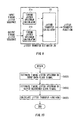
- FIG. 43 shows an eye diagram.
- the horizontal eye opening provides a peak-to-peak value of the timing jitter, while the vertical eye opening provides noise immunity or a signal-to-noise ratio.
- the zero-crossings are caused to jitter by the timing jitter having a peak-to-peak value of 1 UI (Unit Interval, 1 UI is equal to the bit period T b ) or more.
- the eye-diagram measurement can merely measure a closed eye pattern. Therefore, it was difficult to apply the eye diagram to the jitter tolerance measurement.
- FIG. 44 illustrates an exemplary arrangement for the jitter tolerance measurement of the deserializer.
- the jitter tolerance measurement is an extension of the bit error rate test.
- the deserializer performs serial-parallel conversion for the input serial bit stream, so that it outputs the resultant data as, for example, 16-bit recovered data.
- the instantaneous phase ⁇ [nT] of the input bit stream to the deserializer under test is made to fluctuate by the sinusoidal jitter, where T is a data rate.
- a bit error rate tester provides a time delay to the output recovered clock so as to obtain the optimum timing, and samples the output recovered data. By comparing the sampled values of the recovered data with expected values corresponding thereto, the bit error rate of the parallel data is tested.
- the bit error rate tester since the output recovered clock is extracted from the serial bit stream in which edges fluctuate, it becomes difficult to sample the output recovered data at the optimum sampling times when the amount of the incorporated jitter is larger.
- the bit error rate tester has to include a high-performance clock recovery unit. This is because the jitter tolerance measurement of the deserializer requires the clock recovery unit which has larger jitter tolerance than that of the clock recovery unit included in the deserializer under test.
- the minimum incorporated jitter amount that causes generation of the bit error rate is obtained.
- 1-sec bit error rate test is performed by using a pseudo-random binary sequence having a pattern length of 2 15 ⁇ 1. Therefore, in order to change the incorporated jitter amount 20 times and measure the jitter tolerance for each of 20 types of incorporated jitter amount, the test time of 20 sec is required.
- Timing degradation of the input bit stream increases the bit error rate as well as amplitude degradation.
- the timing degradation corresponds to the horizontal eye opening in the eye-diagram measurement
- the amplitude degradation corresponds to the vertical eye opening. Therefore, by measuring the degrees of the timing degradation and amplitude degradation, the bit error rate can be calculated.
- the jitter tolerance measurement corresponds to the horizontal eye opening in the eye-diagram measurement.
- the timing degradation ⁇ T the similar calculation can be performed.
- the % value of the ratio and the dB value are relative values, not absolute values. Thus, in order to obtain an accurate value of the bit error rate, calibration is required.
- an instantaneous bit error rate is calculated from ⁇ A, ⁇ T, a local clock period T and the maximum value A of the samples at the optimum sampling times.
- the invention disclosed in the aforementioned patent merely provides a method for estimating the bit error rate by measuring the timing degradation by a Gaussian noise jitter.
- the invention disclosed in the aforementioned patent obtains a histogram of data edges, performs a threshold operation and obtains ⁇ T.
- This operation is effective to the Gaussian noise jitter having a single peak.
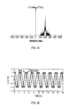
- FIG. 45 compares a probability density function distribution of the Gaussian noise jitter and that of the sinusoidal jitter.
- the sinusoidal jitter used in the jitter tolerance test has two peaks at both ends of the distribution. Therefore, ⁇ T cannot be obtained only by performing the simple threshold operation.
- the zero-crossings are caused to jitter by the timing jitter of 1 UI PP or more.
- the histogram has the distribution in which the probability density functions of adjacent edges overlap each other, as shown in FIG.
- a measuring apparatus for measuring jitter characteristics of an electronic circuit comprises: a timing jitter calculator operable to calculate a first timing jitter sequence of a first signal and a second timing jitter sequence of a second signal, the first signal being supplied to the electronic circuit or generated by the electronic circuit, the second signal being generated by the electronic circuit; and a jitter transfer function estimator operable to calculate a jitter transfer function between the first signal and the second signal based on frequency components of the first and second timing jitter sequences.
- the jitter transfer function estimator may calculate the jitter transfer function based on a ratio of a frequency component of a timing jitter in the first timing jitter sequence and a frequency component of a timing jitter in the second timing jitter sequence, the timing jitter in the first timing jitter sequence and the timing jitter in the second timing jitter sequence having approximately equal frequencies.
- Each of the first and second timing jitter sequences may include a plurality of frequency components, and the jitter transfer function estimator may calculate the jitter transfer function, for a plurality of frequency component pairs each of which is formed by a frequency component of a timing jitter in the first timing jitter sequence and a frequency component of a timing jitter in the second timing jitter sequence which correspond to approximately equal frequencies, based on frequency component ratios of the timing jitters in the first and second timing jitter sequences.
- the timing jitter calculator may calculate the first timing jitter sequence while using an input signal supplied to the electronic circuit as the first signal.
- the first signal may be an input signal supplied to the electronic circuit, and the measuring apparatus may further comprise a jitter incorporating unit operable to incorporate a desired input timing jitter into the input signal.
- the jitter incorporating unit may incorporate the input timing jitter having a plurality of frequency components into the input signal.
- the jitter transfer function estimator may include a timing jitter spectrum calculator operable to receive the first and second timing jitter sequences and to calculate frequency components of the first and second timing jitter sequences.
- the jitter transfer function estimator may include: a power spectrum calculator operable to calculate a power spectrum of the first timing jitter sequence or the second timing jitter sequence; a cross spectrum calculator operable to calculate a cross spectrum between the first timing jitter sequence and the second timing jitter sequence; and a jitter transfer function calculator operable to calculate the jitter transfer function based on a ratio of the power spectrum to the cross spectrum.
- the measuring apparatus may further comprise a jitter related transmission penalty calculator operable to calculate jitter related transmission penalty of the electronic circuit based on the jitter transfer function.
- the jitter related transmission penalty calculator may include a bit error rate calculator operable to calculate a bit error rate of the electronic circuit based on the jitter transfer function.
- the jitter related transmission penalty calculator may include a jitter tolerance calculator operable to calculate jitter tolerance of the electronic circuit based on the jitter transfer function.
- Each of the first and second timing jitter sequences may include a plurality of frequency components, and the bit error rate calculator may calculate a worst-case value of the bit error rate for the plurality of frequency components.
- Each of the first and second timing jitter sequences may include a plurality of frequency components, and the bit error rate calculator may further calculate a mean value of the bit error rate for the plurality of frequency components.
- Each of the first and second timing jitter sequences may includes a plurality of frequency components, and the bit error rate calculator may further calculate the bit error rate in a case where a sinusoidal jitter was incorporated as an input timing jitter into an input signal of the electronic circuit, for the plurality of frequency components.
- the bit error rate calculator may calculate performance limit of the bit error rate of the electronic circuit in the case where the sinusoidal jitter was incorporated as the input timing jitter.
- Each of the first and second timing jitter sequences may include a plurality of frequency components, and the jitter tolerance calculator may calculate a worst-case value of the jitter tolerance for the plurality of frequency components.
- Each of the first and second timing jitter sequences may include a plurality of frequency components, and the jitter tolerance calculator may further calculate a mean value of the jitter tolerance for the plurality of frequency components.
- the jitter tolerance calculator may calculate the jitter tolerance of the electronic circuit in the case where the sinusoidal jitter was incorporated as an input timing jitter.
- the jitter tolerance calculator may calculate performance limit of the jitter tolerance of the electronic circuit in the case where the sinusoidal jitter was incorporated as the input timing jitter.
- the jitter incorporating unit may incorporate the timing jitter into the input signal by performing phase modulation of the input signal.
- the jitter incorporating unit may incorporate the timing jitter into the input signal by performing frequency modulation of the input signal.
- the second signal may be an output signal output from the electronic circuit;
- the jitter incorporating unit may incorporate a plurality of input timing jitters having different amplitudes into the input signal, the amplitudes being within a region where a relationship between the input timing jitters and output timing jitters of the output signal is linear; and the jitter transfer function estimator may include a gain calculator operable to calculate a gain of the jitter transfer function by performing linear approximation of a relationship between timing jitter values in the first timing jitter sequence and timing jitter values in the second timing jitter sequence, the timing jitter values in the first and second timing jitter sequences being made to correspond to the respective amplitudes of the input timing jitters.
- the jitter transfer function estimator may further include a timing phase difference calculator operable to calculate a phase difference between the input timing jitters and the output timing jitters.
- the timing jitter calculator may include: an analytic signal transformer operable to transform the first and second signals to an analytic signal that is a complex number; an instantaneous phase estimator operable to estimate an instantaneous phase of the analytic signal based on the analytic signal; a linear instantaneous phase estimator operable to estimate a linear instantaneous phase of each of the first and second signals based on the instantaneous phase of the analytic signal; and a linear trend remover operable to calculate an instantaneous phase noise, that is obtained by removing the linear instantaneous phase from the instantaneous phase, based on the instantaneous phase and the linear instantaneous phase for each of the first and second signals.
- the timing jitter calculator may further include a resampler operable to receive the instantaneous phase noise of each of the first and second signals and to calculate the first and second timing jitter sequences by resampling the received instantaneous phase noise.
- the resampler may resample the instantaneous phase noise at times approximately the same as zero-crossing times of a corresponding one of the first and second signals.
- the analytic signal transformer may include: a bandwidth limiter operable to extract, from each of the first and second signals, frequency components containing a fundamental frequency of a corresponding one of the first and second signals; and a Hilbert transformer operable to generate, for each of the first and second signals, a Hilbert pair obtained by performing Hilbert transform of the frequency components extracted by the bandwidth limiter, and wherein the analytic signal transformer outputs the Hilbert pair as an imaginary part of the analytic signal.
- the analytic signal transformer may include: a time-domain to frequency-domain transformer operable to transform each of the first and second signals to a two-sided spectrum in frequency domain; a bandwidth limiter operable to extract frequency components of the two-sided spectrum, the frequency components containing a positive fundamental frequency; and a frequency-domain to time-domain transformer operable to output as the analytic signal a signal obtained by transforming the frequency components extracted by the bandwidth limiter into time domain.
- the analytic signal transformer may include: a buffer memory operable to store the first and second signals; a waveform data selector operable to sequentially select a part of the first and second signals stored in the buffer memory; an window function multiplier operable to multiply the signal part selected by the waveform data selector by a predetermined window function; a time-domain to frequency-domain transformer operable to transform the signal part multiplied by the window function to a spectrum in frequency domain; a bandwidth limiter operable to extract frequency components of the spectrum, the frequency components containing a positive fundamental frequency; a frequency-domain to time-domain transformer operable to transform the frequency components extracted by the bandwidth limiter to a time-domain signal; and an amplitude corrector operable to multiply the time-domain signal by a reciprocal of the window function to generate the analytic signal, and wherein the waveform data selector selects the signal part to partially overlap a previously selected signal part.
- the bandwidth limiter may extract a desired frequency band.
- the timing jitter estimator may include an waveform clipper operable to remove amplitude modulation components of the first and second signals and to supply the first and second signals without the amplitude modulation components to the analytic signal transformer.
- the timing jitter calculator may further include a low frequency component remover operable to remove low frequency components of the instantaneous phase noise and to supply the instantaneous phase noise without the low frequency components to the resampler.
- a measuring apparatus for performing a measurement for an electronic circuit comprises: an instantaneous phase noise calculator operable to calculate a first instantaneous phase noise of a first signal and a second instantaneous phase noise of a second signal, the first signal being supplied to the electronic circuit or generated by the electronic circuit, the second signal being generated by the electronic circuit; and a jitter transfer function estimator operable to calculate a jitter transfer function between the first and second signals based on frequency components of the first and second instantaneous phase noises.
- a measuring method for measuring jitter characteristics of an electronic circuit comprises: calculating a first timing jitter sequence of a first signal and a second timing jitter sequence of a second signal, the first signal being supplied to the electronic circuit or generated by the electronic circuit, the second signal being generated by the electronic circuit; and calculating a jitter transfer function between the first and second signals based on frequency components of the first and second timing sequences.
- the measuring method may further comprise calculating jitter related transmission penalty of the electronic circuit based on the jitter transfer function.
- the calculation of jitter related transmission penalty may include calculation of a bit error rate of the electronic circuit based on the jitter transfer function.
- the calculation of jitter related transmission penalty may include calculation of jitter tolerance of the electronic circuit based on the jitter transfer function.
- a measuring method for performing a measurement for an electronic circuit comprises: calculating a first instantaneous phase noise of a first signal and a second instantaneous phase noise of a second signal, the first signal being supplied to the electronic circuit or generated by the electronic circuit, the second signal being generated by the electronic circuit; and calculating a jitter transfer function between the first and second signals based on frequency components of the first and second instantaneous phase noises.
- FIG. 1 illustrates an exemplary arrangement of a measuring apparatus 100 according to an embodiment of the present invention.
- FIG. 2 is a flowchart of an exemplary measuring method according to an embodiment of the present invention.
- FIG. 3 illustrates another exemplary arrangement of the measuring apparatus 100 .
- FIG. 4 illustrates another exemplary arrangement of the measuring apparatus 100 .
- FIG. 5 illustrates other exemplary arrangement of the measuring apparatus 100 .
- FIG. 6 is a flowchart of another exemplary measuring method.
- FIG. 7 illustrates an exemplary arrangement of a timing jitter calculator 10 .
- FIG. 8 is a flowchart of an example of Timing jitter calculation step S 1010 .
- FIG. 9 illustrates an exemplary arrangement of a jitter transfer estimator 20 .
- FIG. 10 is a flowchart of an example of Jitter transfer function estimation step S 1020 .
- FIG. 11 illustrates an exemplary arrangement of an analytic signal transformer 11 .
- FIG. 12 is a flowchart of an example of Analytic signal transforming step S 1011 .
- FIG. 13 shows an example of an output signal.
- FIG. 14 shows an example of a two-sided spectrum.
- FIG. 15 shows an example of a frequency domain signal Z(f) obtained by transform.
- FIG. 16 shows an example of an analytic signal z(t) that was band-limited.
- FIG. 17 shows an example of an instantaneous phase waveform ⁇ (t).
- FIG. 18 shows an example of the continuous instantaneous phase waveform ⁇ (t) that was unwrapped.
- FIG. 19 shows an example of an instantaneous phase noise.
- FIG. 20 shows an example of a timing jitter sequence.
- FIG. 21 shows an example of frequency components of timing jitter sequences of input and output signals and a jitter transfer function.
- FIG. 22 illustrates another exemplary arrangement of the jitter transfer function estimator 20 .
- FIG. 23 is a flowchart of another example of Jitter transfer function estimation step S 1020 .
- FIG. 24 is a flowchart of another example of Jitter transfer function estimation step S 1020 .
- FIG. 25 is a flowchart of another example of Timing jitter calculation step S 1010 .
- FIG. 26 shows an example of an output signal of a DUT.
- FIG. 27 shows an example of the output signal from which amplitude modulation components were removed.
- FIG. 28 illustrates another exemplary arrangement of the timing jitter calculator 10 .
- FIG. 29 is a flowchart of other example of Timing jitter calculation step S 1010 .
- FIG. 30 illustrates another exemplary arrangement of the analytic signal transformer 11 .
- FIG. 31 is a flowchart of another example of Analytic signal transforming step S 1011 .
- FIG. 32 illustrates another exemplary arrangement of the jitter transfer function estimator 20 .
- FIG. 33 shows an exemplary relationship between timing jitter values of the input timing jitter sequence and timing jitter values of the output timing jitter sequence.
- FIG. 34 illustrates another example of the measurement by the measuring apparatus 100 .
- FIG. 35 illustrates an exemplary arrangement of the measuring apparatus 100 shown in FIG. 34 .
- FIG. 36 illustrates another example of the measurement by the measuring apparatus 100 .
- FIG. 37 illustrates an exemplary arrangement of the measuring apparatus 100 shown in FIG. 36 .
- FIG. 38 shows an example of the result of the jitter transfer function measurement performed by the measuring apparatus 100 .
- FIG. 39 shows an example of the result of the bit error rate measurement performed by the measuring apparatus 100 .
- FIG. 40 shows an example of the result of the jitter tolerance measurement performed by the measuring apparatus 100 .
- FIG. 41 shows another example of the result of the jitter tolerance measurement performed by the measuring apparatus 100 .
- FIG. 42 shows an example of the bit error rate measured by the measuring apparatus 100 .
- FIG. 43 shows an eye diagram
- FIG. 44 illustrates an arrangement for a jitter tolerance measurement of a deserializer.
- FIG. 45 compares a probability density distribution of a Gaussian noise jitter with that of a sinusoidal jitter.
- FIG. 1 illustrates an exemplary arrangement of a measuring apparatus 100 according to an embodiment of the present invention.
- the measuring apparatus 100 measures a jitter transfer function in an electronic circuit (DUT) as an example of a system, circuit and device under test.
- DUT electronic circuit
- the measuring apparatus 100 includes a timing jitter calculator 10 and a jitter transfer function estimator 20 .
- the timing jitter calculator 10 calculates the first timing jitter sequence of the first signal and the second timing jitter sequence of the second signal in the DUT.
- Each of the first and second signals may be a signal input to the DUT, a signal output from the DUT or a signal in the DUT.
- the timing jitter sequence in the above is a signal described later referring to FIGS. 13–20 .
- the jitter transfer function estimator 20 calculates a jitter transfer function between the first and second signals based on frequency components of the first and second timing jitter sequences.
- the jitter transfer function estimator 20 may calculate the jitter transfer function based on a ratio of a frequency component of a jitter in the first timing sequence and a frequency component of a jitter in the second timing jitter sequence. Then, the jitter in the first timing sequence and the jitter in the second timing sequence have frequencies approximately equal to each other.
- the jitter transfer function estimator 20 calculates the jitter transfer function based on the frequency component ratios of the jitters in the first and second timing jitter sequences.
- FIG. 2 is a flowchart showing an exemplary measuring method according to an embodiment of the present invention. This measuring method measures the jitter transfer function in the electronic circuit (DUT) as an example of a system, circuit or a device under test.
- DUT electronic circuit
- Timing jitter calculation step S 1010 the timing jitter sequences of the first and second signals in the DUT are calculated.
- Step S 1010 has a similar function to that of the timing jitter calculator 10 described referring to FIG. 1 .
- Step S 1020 the jitter transfer function in the DUT is estimated.
- Step S 1020 has a similar function to that of the jitter transfer function estimator 20 described referring to FIG. 1 .
- FIG. 3 illustrates another exemplary arrangement of the measuring apparatus 100 .
- the measuring apparatus 100 shown in FIG. 3 is different from the measuring apparatus 100 shown in FIG. 1 in that an instantaneous phase noise calculator 30 is provided in place of the timing jitter calculator 10 .
- the instantaneous phase noise calculator 30 calculates an instantaneous phase noise of the first signal and that of the second signal in the DUT. Please note that the instantaneous phase noise is a signal described later referring to FIGS. 13–19 .
- the jitter transfer function estimator 20 calculates the jitter transfer function between the first and second signals based on the frequency components of the jitters in the first and second instantaneous noises, the frequencies of the jitters being approximately equal to each other.
- the jitter transfer function estimator 20 has a similar function to that of the jitter transfer function estimator 20 described referring to FIG. 1 .
- FIG. 4 is another exemplary flowchart showing an exemplary measuring method according to the embodiment of the present invention.
- This measuring method includes Instantaneous phase noise calculation step S 1030 in place of Step S 1010 in the measuring method described referring to FIG. 2 .
- Step S 1030 the instantaneous phase noises of the first and second signals of the DUT are calculated.
- Step S 1060 may have a similar function to that of the instantaneous phase noise calculator 30 described referring to FIG. 3 .
- FIG. 5 illustrates another exemplary arrangement of the measuring apparatus 100 .
- the measuring apparatus 100 receives an input signal and an output signal of the DUT 200 as the first and second signals, respectively.
- the measuring apparatus 100 includes the arrangement of the measuring apparatus 100 described referring to FIG. 1 and further includes a noise source 50 , a jitter incorporating unit 40 and a jitter related transmission penalty calculator 60 .
- the jitter transfer function is measured based on the timing jitter sequences of the signals of the DUT 200 like the measuring apparatus 100 described referring to FIG. 1
- the jitter transfer function may be measured based on the instantaneous phase noises of the signals of the DUT 200 in an alternative example, like the measuring apparatus 100 described referring to FIG. 3 .
- the measuring apparatus 100 in this example incorporates the jitter into the input signal to the DUT and measures at lest one of the jitter transfer function, a bit error rate and jitter tolerance of the DUT based on the input signal with the incorporated jitter and the output signal from the DUT.
- the noise source 50 generates a desired input timing jitter (noise) to be incorporated into the input signal.
- the jitter incorporating unit 40 incorporates the input timing jitter generated by the noise source 50 into the input signal.
- the noise source 50 preferably generates a broadband input timing jitter.
- the noise source 50 generates a Gaussian jitter that has frequency components in the broad band.
- the jitter incorporating unit 40 may incorporate the timing jitter into the input signal by performing phase modulation or frequency modulation of the input signal. In other words, the jitter incorporating unit 40 may modulate phase terms or frequency terms in the input signal by the Gaussian jitter.
- the DUT 200 receives the input signal with the incorporated input timing jitter and outputs the output signal in accordance with the received input signal.
- the input timing jitter incorporated into the input signal is transferred to the output timing jitter of the output signal in accordance with the jitter transfer function of the DUT 200 .
- the timing jitter calculator 10 calculates the timing jitter sequence of the input signal, i.e., the first timing jitter sequence, and that of the output signal, i.e., the second timing jitter sequence.
- the jitter transfer function estimator 20 measures the jitter transfer function based on the first and second timing jitter sequences.
- the jitter related transmission penalty calculator 60 calculates jitter related transmission penalty of the DUT based on the jitter transfer function.
- the jitter related transmission penalty in the present specification means reliability of the DUT's operation with respect to the input timing jitter.
- the jitter related transmission penalty calculator 60 includes a bit error rate calculator 62 which calculates a bit error rate of the DUT and a jitter tolerance calculator 64 which calculates jitter tolerance of the DUT.
- the jitter related transmission penalty of the DUT can be calculated easily.
- the measuring apparatus 100 includes the jitter incorporating unit 40 and the noise source 50 in this example, the jitter incorporating unit 40 and the noise source 50 may be provided in the outside of the measuring apparatus 100 in an alternative example.
- the timing jitter calculator 10 calculates the timing jitter sequence of the input signal.
- the timing jitter sequence of the input signal may be given from the outside to the jitter transfer function estimator 20 .
- the noise source 50 may supply the timing jitter sequence of the input signal to the jitter transfer function estimator 20 .
- FIG. 6 is a flowchart showing another exemplary measuring method.
- the measuring method in this example includes the steps of the measuring method described referring to FIG. 2 and further includes Jitter incorporating step S 1040 and Jitter related transmission penalty calculation step S 1060 .
- Step S 1040 a desired timing jitter is incorporated into the input signal.
- Step S 1040 has a similar function to that of the jitter incorporating unit 40 described referring to FIG. 5 .
- the timing jitter sequences of the input and output signals are calculated in Step S 1010 .
- Step S 1010 has a similar function to that of the timing jitter calculator 10 described referring to FIG. 5 .
- Step S 1020 the jitter transfer function is estimated based on the timing jitter sequences.
- Step S 1020 has a similar function to that of the jitter transfer function estimator 20 described referring to FIG. 5 .
- the jitter related transmission penalty of the DUT is calculated based on the jitter transfer function in Step S 1060 .
- Step S 1060 has a similar function to that of the jitter related transmission penalty calculator 60 described referring to FIG. 5 .
- the details of the operation and arrangement of the measuring apparatus 100 and the details of the measuring method are described below.
- FIG. 7 illustrates an exemplary arrangement of the timing jitter calculator 10 .
- the timing jitter calculator 10 includes an analytic signal transformer 11 , an instantaneous phase estimator 12 , a linear instantaneous phase estimator 13 , a linear trend remover 14 and a resampler 15 .
- the timing jitter calculator 10 calculates the timing jitter sequence of the output signal of the DUT.
- the similar description can be applied to another case where the timing jitter calculator 10 calculates the timing jitter sequence of the input signal.
- the measuring apparatus 100 may include the timing jitter calculator 10 for each of the input and output signals.
- the analytic signal transformer 11 receives the output signal and transforms the received output signal to an analytic signal that is a complex number.
- the analytic signal transformer 11 generates the analytic signal by, for example, Fourier transform or Hilbert transform.
- the instantaneous phase estimator 12 receives the analytic signal and estimates an instantaneous phase of the received analytic signal.
- the linear instantaneous phase estimator 13 estimates a linear instantaneous phase of the output signal based on the instantaneous phase of the analytic signal.
- the linear trend remover 14 calculates an instantaneous phase noise obtained by removing the linear instantaneous phase from the instantaneous phase based on the instantaneous phase and the linear instantaneous phase.
- the resampler 15 receives the instantaneous phase noise and calculates the timing jitter sequence of the output signal by resampling the received instantaneous phase noise. For example, the resampler 15 may resample the instantaneous phase noise at times approximately the same as the zero-crossing times of the output signal. That is, the instantaneous phase noise may be resampled based on the zero-crossing times of a real part of the analytic signal.
- the timing jitter sequence indicating the jitters at the edges of the output signal can be easily generated.
- FIG. 8 is a flowchart showing an example of Timing jitter calculation step S 1010 .
- Analytic signal transforming step S 1011 the output signal, that was input, is transformed to the analytic signal.
- Step S 1011 has a similar function to that of the analytic signal transformer 11 described referring to FIG. 7 .
- Instantaneous phase estimation step S 1012 the instantaneous phase of the analytic signal is estimated.
- Step S 1012 has a similar function to that of the instantaneous phase estimator 12 described referring to FIG. 7 .
- Step S 1013 the linear instantaneous phase is estimated.
- Step S 1013 has a similar function to that of the linear instantaneous phase estimator 13 described referring to FIG. 7 .
- Step S 1014 the instantaneous phase noise, that is obtained by removing the linear components from the instantaneous phase, is estimated.
- Step S 1014 has a similar function to that of the linear trend remover 14 described referring to FIG. 7 .
- Resampling step S 1015 the instantaneous phase noise is resampled, so as to estimate the timing jitter sequence.
- Step S 1015 has a similar function to that of the resampler 15 described referring to FIG. 7 .
- FIG. 9 illustrates an exemplary arrangement of the jitter transfer function estimator 20 .
- the jitter transfer function estimator 20 includes a plurality of timing jitter spectrum calculators 21 that are provided for the input signal and the output signal, respectively, and a jitter transfer function calculator 23 .
- Each timing jitter spectrum calculator 21 calculates frequency components of the timing jitter sequence of the associated one of the input and output signals.
- the timing jitter spectrum calculator 21 calculates the frequency components of the timing jitter sequence by, for example, Fourier transform.
- the jitter transfer function calculator 23 calculates the jitter transfer function based on a ratio of the frequency component of the jitter in the timing jitter sequence of the input signal and the frequency component of the jitter in the timing jitter sequence of the output signal, the frequencies of both the jitters being approximately equal to each other.
- the timing jitter having Gaussian distribution is incorporated into the input signal, the timing jitter sequences of the input and output signal have the frequency components that are not substantially zero in a broad band.
- the ratios of the frequency components can be calculated for a plurality of frequencies by a single measurement, so that the jitter transfer function can be calculated.
- the jitter transfer function can be calculated in a case where a sinusoidal jitter is incorporated into the input signal.
- a ratio of the frequency components at a single frequency can be calculated by a single measurement.
- FIG. 10 is a flowchart showing an example of Jitter transfer function estimation step S 1020 .
- Jitter transfer function estimation step S 1020 includes Input timing jitter spectrum calculation step S 1021 , Output timing jitter spectrum calculation step S 1022 and Jitter transfer function calculation step S 1023 .
- Steps S 1021 and S 1022 the frequency components of the timing jitter sequences of the input and output signals are calculated, respectively.
- Each of Steps S 1021 and S 1022 may have a similar function to that of the timing jitter spectrum calculator 21 described referring to FIG. 9 .
- either one of Steps S 1021 and S 1022 may be performed prior to the other.
- both Steps S 1021 and S 1022 may be performed at the same time.
- Step S 1023 the jitter transfer function is calculated.
- Step S 1023 has a similar function to that of the jitter transfer function calculator 23 described referring to FIG. 9 .
- FIG. 11 illustrates an exemplary arrangement of the analytic signal transformer 11 .
- the analytic signal transformer 11 includes a buffer memory 101 for storing a received signal; an waveform data selector 102 for sequentially selecting a part of the signal stored in the buffer memory 101 ; an window function multiplier 103 for multiplying the signal part selected by the waveform data selector 102 by a predetermined window function; a time-domain to frequency-domain transformer 104 for transforming the signal part multiplied by the window function to a spectrum in frequency domain; a bandwidth limiter 106 for extracting frequency components around a fundamental frequency of a given signal; a frequency-domain to time-domain transformer 107 for transforming the frequency components extracted by the bandwidth limiter 106 to a signal in time domain; and an amplitude corrector 108 for multiplying the signal in time domain by a reciprocal of the window function so as to generate the analytic signal.
- the waveform data selector 102 selects the partial signal in such a manner that the currently selected partial signal partially overlaps the previously selected partial signal.
- amplitude modulation is performed for the signal x(t).
- the amplitude modulation of the signal x(t) can be corrected by multiplying by the reciprocal of the window function in the amplitude corrector 108 .
- the window function multiplier 103 outputs a signal x(t) ⁇ w(t) obtained by multiplying the signal x(t) by the window function w(t) to the time-domain to frequency-domain transformer 104 .
- the time-domain to frequency-domain transformer 104 transforms the received signal to a signal in frequency domain, and the bandwidth limiter 106 then outputs a spectrum Z(f) obtained by changing the negative frequency components of the frequency-domain signal to zero.
- the frequency-domain to time-domain transformer 107 outputs a signal IFFT[Z(f)], that was obtained by transforming the spectrum Z(f) to a signal in time domain.
- the analytic signal transformer 11 may output a real part and an imaginary part of the signal output from the frequency-domain to time-domain transformer 107 as the real part and the imaginary part of the analytic signal, respectively.
- the real and imaginary parts of the analytic signal are assumed to be x real (t) and x imag (t), respectively, they have the following relationship with the real and imaginary parts of the output signal from the frequency-domain to time-domain transformer 107 , Re ⁇ IFFT[Z(f)] ⁇ and Im ⁇ IFFT[Z(f)] ⁇ .
- w′(t) represents components of the window function (t) in the spectrum Z(f).
- the real part x real (t) and the imaginary part x imag (t) of the analytic signal are influenced by the amplitude modulation by the window function w(t) to substantially the same degree.
- the instantaneous phase of the signal x(t) is represented by the following expression.
- ⁇ ⁇ ( t ) tan - 1 ⁇ [ w ′ ⁇ ( t ) w ⁇ ( t ) ⁇ x real ⁇ ( t ) w ′ ⁇ ( t ) w ⁇ ( t ) ⁇ x imag ⁇ ( t ) ] - 2 ⁇ ⁇ ⁇ ⁇ f j ⁇ t ⁇ tan - 1 ⁇ [ x real ⁇ ( t ) x imag ⁇ ( t ) ] - 2 ⁇ ⁇ ⁇ ⁇ f j ⁇ t ( 3 )
- a phase estimation error caused by the amplitude modulation by the window function can be cancelled in the real and imaginary parts in a case of calculating the instantaneous phase of the signal x(t).
- the phase estimation error is generated by the amplitude modulation as follows.
- ⁇ ⁇ ( t ) tan - 1 ⁇ [ w ′ ⁇ ( t ) w ⁇ ( t ) ⁇ x ⁇ ⁇ ( t ) x ⁇ ( t ) ] - 2 ⁇ ⁇ ⁇ ⁇ f j ⁇ t ( 4 )
- the instantaneous phase in which the phase estimation error by the amplitude modulation by the window function was removed can be calculated.
- the instantaneous phase estimator 12 can calculate the instantaneous phase of the signal x(t) with high precision.
- the buffer memory 101 stores a signal to be measured.
- the waveform data selector 102 selects and extracts a part of the signal stored in the buffer memory 101 .
- the window function multiplier 103 then multiplies the partial signal selected by the waveform data selector 102 by the window function.
- the time-domain to frequency-domain transformer 104 then performs FFT for the partial signal multiplied by the window function, so as to transform the time-domain signal to a two-sided spectrum in frequency domain.
- the bandwidth limiter 106 then replaces the negative frequency components of the two-sided spectrum in frequency domain with zero, and thereafter replaces frequency components other than the frequency components in the vicinity of a fundamental frequency of the signal to be measured with zero, thereby band-limiting the frequency-domain signal.
- the frequency-domain to time-domain transformer 107 performs inverse FFT for the one-sided spectrum in frequency domain, that was band-limited, so as to transform the frequency-domain signal to a time-domain signal.
- the amplitude corrector 108 then multiplies the time-domain signal obtained by inverse transform by the reciprocal of the window function, so as to generate the band-limited analytic signal.
- the analytic signal transformer 11 checks whether or not any unprocessed data is left in the buffer memory 101 .
- the waveform data selector 102 selects and extracts a next part of the signal stored in the buffer memory 101 . After the waveform data selector 102 selected and extracted the partial signal sequentially in such a manner that the currently selected partial signal overlaps the previously selected partial signal, the analytic signal transformer 11 repeats the aforementioned procedure.
- FIG. 12 is a flowchart showing an example of the analytic signal transform step S 1011 .
- Buffer memory step S 1101 the input signal or the output signal is stored.
- Step S 1101 has a similar function to that of the buffer memory 101 described referring to FIG. 11 .
- Waveform data selection step S 1102 a section of the signal stored in Step S 1101 is selected and extracted.
- Step S 1102 has a similar function to that of the waveform data selector 102 described referring to FIG. 11 .
- Step S 1103 the section selected in Step S 1102 by a predetermined window function.
- Step S 1103 may multiply the section, i.e., the partial signal, by Hanning function as the window function.
- Step S 1103 has a similar function to that of the window function multiplier 103 described referring to FIG. 11 .
- Step S 1104 the signal multiplied by the window function is transformed from time domain to frequency domain.
- Step S 1104 has a similar function to that of the time-domain to frequency-domain transformer 104 described referring to FIG. 11 .
- Step S 1105 negative frequency components of the signal transformed from time domain to frequency domain are removed.
- Step S 1105 has a similar function to that of the bandwidth limiter 106 described referring to FIG. 11 .
- Step S 1106 frequency components in the vicinity of the fundamental frequency of the transformed signal are extracted.
- Step S 1106 has a similar function to that of the bandwidth limiter 106 described referring to FIG. 11 .
- Step S 1107 the band-limited signal is transformed to a signal in time domain.
- Step S 1107 has a similar function to that of the frequency-domain to time-domain transformer 107 described referring to FIG. 11 .
- Step S 1108 amplitude modulation components of the signal transformed from frequency domain to time domain are removed.
- Step S 1108 has a similar function to that of the amplitude corrector 108 described referring to FIG. 11 .
- Step S 1109 it is determined whether or not unprocessed data of the signal to be measured that was stored in Step S 1101 is left.
- the next section of the signal is extracted in Waveform data selection step S 1110 in such a manner that the next section partially overlaps the previously extracted section.
- Step S 1110 has a similar function to that of Step S 1102 .
- the procedure is finished.
- a calculation method of the timing jitter sequence in the timing jitter calculator 10 is described referring to a case of the output signal as an example.
- FIG. 13 shows an exemplary output signal.
- the output signal x(t) shown in FIG. 13 is preferably supplied to the timing jitter calculator 10 after being digitized.
- the time-domain to frequency-domain transformer 104 performs Fast Fourier Transform for the output signal, for example, so as to calculate a two-sided spectrum (having positive and negative frequency components) of the output signal X(f).
- FIG. 14 shows an exemplary two-sided spectrum.
- the bandwidth limiter 106 replaces the frequency components other than the positive frequency components in the vicinity of the fundamental frequency of the two-sided spectrum X(f) with zero so as to leave only the positive frequency components in the vicinity of the fundamental frequency and thereafter doubles the left positive frequency components.
- These operations performed in frequency domain correspond to band-limiting the signal to be measured in time domain and transforming the band-limited signal to the analytic signal.
- FIG. 15 shows an exemplary frequency-domain signal Z(f) obtained by transforming the signal X(f).
- the frequency-domain to time-domain transformer 107 then performs inverse Fast Fourier Transform for the signal Z(f) so as to calculate the band-limited analytic signal z(t).
- FIG. 16 shows an exemplary band-limited analytic signal z(t).
- Transform to the analytic signal using FFT is described in J. S. Bendat and A. G. Piersol, Random Data: Analysis and Measurement Procedure, 2nd edition, John Wiley & Sons, Inc., 1986, for example.
- the operation for doubling the positive frequency components can be omitted in a case where the objective is to calculate the instantaneous phase.
- the obtained analytic signal has been subjected to the band-pass filtering operation. This is because only the signal components in the vicinity of the fundamental frequency of the signal to be measured are processed in jitter analysis since the jitter corresponds to the fluctuation of the fundamental frequency of the signal to be measured.
- the instantaneous phase estimator 12 estimates the instantaneous phase from the analytic signal.
- the instantaneous phase waveform ⁇ (t) of the real signal x(t) can be calculated from the analytic signal z(t) in accordance with the following equation.
- the calculated instantaneous phase is represented with the following equation.
- ⁇ ⁇ ( t ) [ 2 ⁇ ⁇ T 0 ⁇ t + ⁇ 0 - ⁇ ⁇ ( t ) ] ⁇ ⁇ mod ⁇ ⁇ 2 ⁇ ⁇ ⁇ [ rad ] ( 6 )
- ⁇ (t) is represented by using a principal value having a phase in the range from ⁇ to + ⁇ and has a discontinuous point near a changing point at which ⁇ (t) changes from + ⁇ to ⁇ .
- FIG. 17 shows an exemplary instantaneous phase waveform ⁇ (t).
- the discontinuous instantaneous phase waveform ⁇ (t) that is, appropriately adding an integral multiple of 2 ⁇ to the principal value ⁇ (t)
- the discontinuity can be removed so that a discontinuous instantaneous waveform ⁇ (t) is obtained.
- FIG. 18 shows an example of the unwrapped continuous instantaneous phase waveform ⁇ (t).
- the linear instantaneous phase estimator 13 estimates the linear instantaneous phase based on the unwrapped instantaneous phase. Please note the linear instantaneous phase described here is an instantaneous phase of an ideal signal having no jitter. That is, the linear instantaneous phase estimator 13 calculates linear components of the instantaneous phase. Then, the linear trend remover 14 generates the instantaneous phase noise obtained by removing the linear instantaneous phase from the instantaneous phase.
- FIG. 19 shows an example of the instantaneous phase noise. Then, the resampler 15 resamples the instantaneous phase noise at the zero-crossing times of the real part of the analytic signal, thereby generating the timing jitter sequence.
- FIG. 20 shows an example of the timing jitter sequence. Then, the jitter transfer function estimator 20 calculates the jitter transfer function based on the timing jitter sequences of the input signal and the output signal. Each of the timing jitter spectrum calculators 21 performs Fourier Transform for the timing jitter sequence of the corresponding one of the input and output signals, so as to calculate the frequency components.
- FIG. 21 shows an example of the frequency components of the timing jitter sequences of the input and output signals and an example of the jitter transfer function.
- the jitter transfer function calculator 23 calculates a ratio of the frequency component of the input timing jitter sequence and the frequency component of the output timing jitter, both the frequency components corresponding to frequencies approximately equal to each other. For example, in the input timing jitter sequence, the frequency components indicated with a, b, c, d and e are calculated. Similarly, in the output timing jitter sequence, the frequency components indicated with a′, b′, c′, d′ and e′ are calculated.
- the jitter transfer function calculator 23 may calculate the jitter transfer function in a necessary frequency region. In this example, the jitter transfer function calculator 23 calculates the frequency component ratio for each of five frequencies. In an another example, however, it is preferable that the frequency component ratio be calculated for more frequencies so that the jitter transfer function is calculated based on the thus calculated frequency component ratios.
- the jitter transfer function at a desired frequency can be calculated efficiently.
- the jitter transfer function estimator may discriminate the frequencies to estimate the jitter transfer function between the input and output timing jitters at each jitter frequency, or may estimate a mean value of the jitter transfer function in a desired frequency region without discriminating the frequencies.
- the jitter transfer function estimator may include a unit operable to obtain the mean value of the jitter transfer function in the desired frequency region.
- the jitter transfer function estimator 20 may output a reciprocal of the calculated jitter transfer function as the jitter transfer function when a gain of the estimated jitter transfer function is larger than 1.0. Also, the jitter transfer function estimator 20 may include a unit operable to calculate the reciprocal of the jitter transfer function.
- FIG. 22 illustrates another exemplary arrangement of the jitter transfer function estimator 20 .
- the jitter transfer function estimator 20 includes timing jitter spectrum calculators 24 a and 24 b , a power spectrum calculator 26 , a cross spectrum calculator 27 and a jitter transfer function calculator 23 .
- the timing jitter spectrum calculators 24 a and 24 b have the same or similar function and arrangement as/to that of the timing jitter spectrum calculator 21 described referring to FIG. 9 .
- the power spectrum calculator 26 calculates a power spectrum of the input signal based on a spectrum of the timing jitter sequence of the input signal.
- the power spectrum calculator 26 may calculate a power spectrum of the timing jitter sequence of the output signal.
- the cross spectrum calculator 27 calculates a cross spectrum of the input and output timing jitter sequences based on the spectra of the timing jitter sequences of the input and output signals.
- the jitter transfer function calculator 23 calculates the jitter transfer function based on a ratio of the power spectrum calculated by the power spectrum calculator 26 to the cross spectrum calculated by the cross spectrum calculator 27 .
- the jitter transfer function calculator 23 calculates the jitter transfer function in accordance with the following equation.
- H J [f J ] represents the jitter transfer function
- ⁇ (f J 9 represents the spectrum of the output timing jitter
- H J [f J ] represents the jitter transfer function
- ⁇ (f J 9 represents the spectrum of the output timing jitter
- ⁇ [f j ] represents the spectrum of the input timing jitter.
- FIG. 23 is a flowchart showing another example of Jitter transfer function estimation step S 1020 .
- Steps S 1024 and S 1025 the spectrum of the input timing jitter sequence and the spectrum of the output timing jitter sequence are respectively generated.
- Steps S 1024 and S 1025 have similar functions to those of the timing jitter spectrum calculators 24 a and 24 b described referring to FIG. 22 .
- Step S 1026 the power spectrum of the input timing jitter sequence is calculated.
- Step S 1026 has a similar function to that of the power spectrum calculator 26 described referring to FIG. 22 .
- Step S 1027 the cross spectrum between the input timing jitter sequence and the output timing jitter sequence is calculated.
- Step S 1027 has a similar function to that of the cross spectrum calculator 27 described referring to FIG. 22 .
- Step S 1028 the jitter transfer function is calculated.
- Step S 1028 has a similar function to that of the jitter transfer function calculator 23 described referring to FIG. 22 .
- FIG. 24 illustrates another exemplary arrangement of the timing jitter calculator 10 .
- the timing jitter calculator 10 includes the arrangement of the timing jitter calculator described referring to FIG. 7 and further includes a waveform clipper 16 .
- the waveform clipper 16 removes the amplitude modulation components of the signal the timing jitter calculator 10 received and supplies the resultant signal to the analytic signal transformer.
- the jitter caused only by the phase modulation components can be detected by removing amplitude modulation components of the input and output signals.
- the bit error rate or the like can be calculated with high precision.
- FIG. 25 is a flowchart showing another example of Timing jitter calculation step S 1010 .
- Step S 1010 in the present example includes Waveform clipping step S 1016 in addition to Step S 1010 described referring to FIG. 8 .
- Step S 1016 the amplitude modulation components of the input signal and the output signal are removed.
- Step S 1016 has a similar function to that of the waveform clipper 16 described referring to FIG. 24 .
- FIGS. 26 and 27 are diagrams explaining the operation of the waveform clipper 16 .
- FIG. 26 shows an example of the output signal from the DUT.
- the waveform clipper 16 multiplies signal values of the output signal by a predetermined value. When the value obtained by the multiplication is larger than a predetermined threshold value, the value obtained by the multiplication is replaced with the predetermined value. In this way, the amplitude modulation component can be removed.
- FIG. 27 shows an example of the output signal from which the amplitude modulation components were removed.
- FIG. 28 illustrates another exemplary arrangement of the timing jitter calculator 10 .
- the timing jitter calculator 10 includes the arrangement of the timing jitter calculator 10 described referring to FIG. 7 and further includes a low frequency component remover 17 .
- the low frequency component remover 17 outputs the instantaneous phase noise after removing from the instantaneous phase noise the low frequency components thereof. By removing the low frequency components of the instantaneous phase noise, the gain of the jitter transfer function can be calculated with higher precision.
- FIG. 29 is a flowchart showing another example of Timing jitter calculation step S 1010 .
- Step S 1010 in the present example includes Low frequency component removing step S 1017 in addition to Step S 1010 described referring to FIG. 8 .
- Step S 1017 removes the low frequency components of the instantaneous phase noise.
- Step S 1017 has a similar arrangement to that of the low frequency component remover 17 described referring to FIG. 28 .
- FIG. 30 illustrates another exemplary arrangement of the analytic signal transformer 11 .
- the analytic signal transformer 11 includes a band-pass filter 111 and a Hilbert transformer 112 .
- the band-pass filter 111 generates a band-limited signal obtained by extracting the frequency components around the fundamental frequency of the input or output signal.
- the band-pass filter 111 may be an analog filter or a digital filter, or may be implemented by digital signal processing such as FFT. Moreover, the band-pass filter 111 may be formed so as to allow the pass band to be freely changed.
- the Hilbert transformer 112 performs Hilbert transform for the band-limited signal so as to generate a Hilbert pair.
- the analytic signal transformer 11 outputs the band-limited signal as the real part of the analytic signal and also outputs the Hilbert pair as the imaginary part of the analytic signal.
- the analytic signal transformer 11 in the present example the analytic signal based on the fundamental frequency of the received signal can be generated.
- the jitter transfer function can be calculated with high precision.
- the generation of the analytic signal using Hilbert transform is described.
- the analytic signal z(t) of the real signal x(t) is defined by the following complex signal. z ( t ) ⁇ x ( t )+ j ⁇ circumflex over (x) ⁇ ( t ) (10) Please note that j is an imaginary unit and an imaginary part ⁇ circumflex over (x) ⁇ (t) of the complex signal z(t) is Hilbert transform of the real part x(t).
- Hilbert transform of the time-domain waveform x(t) is defined by the following equation.
- ⁇ circumflex over (x) ⁇ (t) is convolution of the functions x(t) and (1/ ⁇ t). That is, Hilbert transform is equivalent to the output obtained when x(t) is made to pass through an all-band-pass filter.
- the output ⁇ circumflex over (x) ⁇ (t) is the same in the magnitude of the spectrum component, the phase thereof is shifted by ⁇ /2.
- the instantaneous phase waveform ⁇ (t) of the real signal x(t) is obtained from the analytic signal z(t) in accordance with the following equation.
- ⁇ ⁇ ( t ) tan - 1 ⁇ [ x ⁇ ⁇ ( t ) x ⁇ ( t ) ] ( 12 )
- the output signal x(t) is given by the following equation.
- the thus obtained analytic signal has been subjected to the band-pass filtering by the band-pass filter 111 .
- the jitter corresponding to the fluctuation of the fundamental frequency of the signal to be measured can be calculated with high precision.
- FIG. 31 is a flowchart showing another example of Analytic signal transforming step S 1011 .
- Step S 1011 includes Band-pass filtering step S 1111 , Hilbert transform step S 1112 and Output step S 1113 .
- Step S 1111 the band-limited signal, that is obtained by limiting the band of the input or output signal, is generated in Step S 1111 .
- Step S 1111 has a similar function to that of the band-pass filter 111 described referring to FIG. 30 .
- Step S 1112 the Hilbert pair of the band-limited signal is generated.
- Step S 1112 has a similar function to that of the Hilbert transformer 112 described referring to FIG. 30 .
- Step S 1113 the band-limited signal is output as the real part of the analytic signal, while the Hilbert pair is output as the imaginary part of the analytic signal.
- FIG. 32 illustrates another exemplary arrangement of the jitter transfer function estimator 20 .
- the jitter transfer function estimator 20 includes a gain calculator 501 and a timing phase difference calculator 502 .
- the jitter incorporating unit 40 incorporates a plurality of input timing jitters having different amplitudes from each other into the input signal.
- the gain calculator 501 performs linear fitting (linear approximation) of the timing jitter values in the input timing jitter sequence and the timing jitter values in the output timing jitter sequence, both of which are made to correspond to the respective amplitudes of the input timing jitters, straight line in a linear operation region of the DUT, so as to calculate the gain of the jitter transfer function. That is, the gain calculator 501 calculates the gain of the jitter transfer function by performing the linear approximation of a relationship between the timing jitter values of the first timing jitter sequence and the timing jitter values of the second timing jitter sequence, both of which are made to correspond to the respective amplitude of the input timing jitters.
- FIG. 33 shows an exemplary relationship between the timing jitter values of the input timing jitter sequence and those of the output timing jitter sequence.
- circles represent actual measured values, while straight line represents a result of linear fitting of the actual measured values.
- the gain calculator 501 calculates a slope of this straight line as the gain of the jitter transfer function. Moreover, the gain calculator 501 performs linear fitting of the actually measured values in the region where the DUT linearly operates. For example, the linear fitting is performed in a region where the input timing jitter value is one or less, as shown in FIG. 33 , thereby calculating the gain of the jitter transfer function.
- FIG. 34 illustrates another example of the measurement by the measuring apparatus 100 .
- the DUT 200 includes a clock generator 202 that generates a clock based on the input signal of the DUT; the first circuit 204 that receives the first distributed clock; and the second circuit 206 that receives the second distributed clock.
- the first and second distributed clocks may be clocks of the same frequency, or clocks having multiple frequencies.
- the clock generator 202 is a PLL and generates the clock with a jitter.
- the measuring apparatus 100 in the present example performs the measurement while using the first distributed clock received by the first circuit 204 and the second distributed clock received by the second circuit 206 as the first and second signals, respectively.
- FIG. 35 illustrates an exemplary arrangement of the measuring apparatus 100 shown in FIG. 34 .
- the measuring apparatus 100 includes the timing jitter calculator 10 , the jitter transfer function estimator 20 and the jitter related transmission penalty calculator 60 .
- the timing jitter calculator 10 receives the first and second distributed clocks, calculates the first timing jitter sequence based on the first distributed clock and calculates the second timing jitter sequence based on the second distributed clock.
- the timing jitter calculator 10 has the same or similar function and arrangement as/to that of the timing jitter calculator 10 described referring to FIG. 5 .
- the jitter transfer function estimator 20 calculates the jitter transfer function between the first and second distributed clocks.
- the jitter transfer function estimator 20 has the same or similar function and arrangement as/to that of the jitter transfer function estimator 20 described referring to FIG. 5 .
- the jitter related transmission penalty calculator 60 includes the arrangement of the jitter related transmission penalty calculator 60 described referring to FIG. 5 and further includes a skew calculator 66 .
- the skew calculator 66 calculates a skew between the first circuit 202 and the second circuit 204 based on the jitter transfer function.
- the mean square value of the gain of the jitter transfer function from the gain value of 1.0 is in proportion to energy of the clock skew.
- clock slew can be calculated based on the gain of the jitter transfer function.
- the skew calculator 66 calculates an effective value of the clock skew in accordance with the following equation.
- T SKEW 1 L ⁇ ⁇ (
- the right-hand side of Equation (16) represents the mean square value of the gain of the jitter transfer function from the gain value of 1.0.
- an error rate between the first circuit 204 and the second circuit 206 can be easily calculated by means of a bit error rate calculator 62 .
- FIG. 36 illustrates another example of the measurement by the measuring apparatus 100 .
- the DUT 200 has a synchronous circuit that outputs a data signal and a clock signal to be synchronized with the data signal.
- the measuring apparatus 100 measures the jitter related transmission penalty of the synchronous circuit while using the data signal and the clock signal that are output from the synchronous circuit as the first signal and the second signal, respectively.
- FIG. 37 illustrates an exemplary arrangement of the measuring apparatus 100 shown in FIG. 36 .
- the measuring apparatus 100 includes the timing jitter calculator 10 , the jitter transfer function estimator 20 and the jitter related transmission penalty calculator 60 .
- the measuring apparatus 100 of the present example has the same or similar function and arrangement as/to that of the measuring apparatus 100 described referring to FIG. 35 . According to the measuring apparatus 100 of the present example, the error rate between the data signal and the clock signal can be easily calculated by means of the bit error rate calculator 62 .
- T S is a sampling period
- f J is a jitter frequency that is an offset frequency from the clock frequency.
- the jitter transfer function is given as a frequency response function of a constant-parameter linear system.
- a peak-to-peak value of the input timing jitter is amplified by the gain
- the jitter transfer function is measured from a ratio of the peak-to-peak values or mean values of the input and output jitters. Next, a method for measuring the gain of the jitter transfer function in frequency domain and time domain is discussed.
- the gain of the jitter transfer function can be estimated from the peak-to-peak value or mean value of the timing jitter spectrum (phase noise spectrum) in frequency domain.
- the jitter transfer function is given as the frequency response function of the constant-parameter linear system, the jitter transfer function is not a function of the input to the system. Based on this fact, a procedure for estimating the jitter transfer function in time domain is described. First, the peak-to-peak value of the input timing jitter is set in a region in which the operation of the clock recovery unit under test is linear operation, and then the input/output relationship between ⁇ [nT] and ⁇ [nT] plural times. Thereafter, the input/output relationship of the peak-to-peak jitter between ⁇ [nT] and ⁇ [nT] or the input/output relationship of the RMS jitter is subjected to linear fitting, as shown in FIG. 33 . From the slope of the straight line, the gain of the jitter transfer function is obtained.
- the jitter transfer function in a case of obtaining the jitter transfer function without performing linear fitting, it is not necessary to perform the measurement of the input/output relationship between ⁇ [nT] and ⁇ [nT] plural times for one frequency. Thus, the jitter transfer function can be calculated faster.
- ⁇ PP ⁇ PP ⁇ square root over ([
- An input bit stream to the DUT is given at a bit rate of f bit .
- the DUT is a deserializer that outputs N parallel bits at a data rate of f bit /N parallel . It is assumed that ⁇ [nT] and ⁇ [nT] are transformed into frequency domain by L-point Fourier transform so that the input timing jitter spectrum ⁇ [f J ] and the output timing jitter spectrum ⁇ [f J ] are obtained, for example.
- the frequency-resolutions are given by the following equations, respectively.
- L N parallel lines can be measured by transforming ⁇ [nT] and ⁇ [nT] into frequency domain by L-point Fast Fourier transform.
- ⁇ [nT] and ⁇ [nT] are transformed into frequency domain by N parallel L-point Fast Fourier transform and L-point Fast Fourier transform, respectively, the frequency-resolutions of the input timing jitter spectrum ⁇ [f J ] and the output timing jitter spectrum ⁇ [f J ] are represented by the following equations.
- the speed of the measurement can be increased about L times. It is preferable that the jitter transfer function estimator 20 calculate the jitter transfer function in the above manner. This condition of Fast Fourier transform is reasonable with respect to the causal relationship. This is because both the input timing jitter sequence and the output timing jitter sequence are observed for a time period of TN parallel L and therefore the causal relationship is established between them.
- a PLL incorporated in the deserializer under test includes a frequency divider therein.
- the division ratio N division of the frequency divider used in the deserializer is typically designed to be equal to the number of bits output in parallel, N parallel .
- the alignment jitter is defined as the amount in time domain.
- y ⁇ ( t ) B ⁇ ⁇ sin ⁇ ( 2 ⁇ ⁇ ⁇ f bit N parallel ⁇ t + ⁇ ⁇ ⁇ ⁇ [ t ] ) ( 37 )
- f bit is a bit rate (bit clock frequency).
- f bit /N parallel is a data rate of the recovered clock.
- ⁇ [nT] of x(t) a sinusoidal jitter and a Gaussian noise jitter are known.
- a pseudo-random sequence is also included in the Gaussian noise jitter.
- the instantaneous phase ⁇ [nT] of the bit clock is changed by a sine wave cos (2 ⁇ f PM t).
- the input data stream to the DUT has the following timing jitter.
- ⁇ [ nT] K i cos (2 ⁇ f PM t )
- t nT (38)
- 2K i is a peak-to-peak value of the input jitter
- f PM is a phase modulation frequency by the sine wave.
- the sinusoidal jitter gives the DUT a deterministic jitter.
- the probability density distribution of the sinusoidal jitter corresponds to the worst case.
- 2K i is a peak-to-peak value of the input jitter.
- H J (f) is the jitter transfer function of the DUT.
- the sinusoidal jitter When the jitter transfer function of the clock recovery unit is measured, the sinusoidal jitter has been conventionally used.
- the sinusoidal jitter makes the instantaneous phase of the bit clock, ⁇ [nT] or ⁇ [nT] correspond to the sine wave cos(2 ⁇ f PM t).
- the sinusoidal jitter when the sinusoidal jitter is demodulated, the sine wave is obtained. Since this sine wave corresponds to a line spectrum in frequency domain, the jitter frequency f J is given as a single frequency f PM . Therefore, in order to measure the jitter transfer function by using the sinusoidal jitter, it is necessary to sweep the frequency f PM of the sine wave K sweep times from f lower to f upper .
- the measurement time of the jitter transfer function when the sinusoidal jitter is incorporated is obtained.
- the sampling of the sinusoidal jitter is performed for a period corresponding to M cycle periods (20 periods, for example). This requires observation time of M cycle /f J .
- the digitized waveform thus obtained is subjected to Fast Fourier transform (4 k or 8 k-point Discrete Fourier transform, for example), so that the timing jitter sequence of the digitized waveform is obtained. That is, a product of calculation time of Fast Fourier transform T FFT and the number N FFT of sections of overlap-save sectioning (40, for example) dominates total calculation time.
- the total calculation time that is required for obtaining the timing jitter sequences from the digitized waveforms of the input and output is given by T FFT N FFT .
- the relationship between the input and output timing jitter values is subjected to linear fitting, thereby obtaining the gain of the jitter transfer function.
- the amplitude of the sinusoidal jitter is changed four times, and the jitter transfer function is measured for each of four amplitudes of the sinusoidal jitter.
- the sum of the observation time and the total calculation time is multiplied by a constant, 4.
- the resultant is multiplied by the number of the frequency sweep times K sweep . Accordingly, the total measurement time is given by the following equation.
- the Gaussian noise waveform is obtained. Since the Gaussian noise corresponds to a broadband spectrum in frequency domain, the frequency sweep in the offset frequency section (f lower , f upper ) is not necessary. The jitter transfer functions in the offset frequency section (f lower , f upper ) can be measured simultaneously.
- the total measurement time is obtained in a similar manner.
- sampling of the Gaussian noise jitter is performed for a period corresponding to M cycle periods. This requires observation time of M cycle /f lower .
- the digitized waveform thus obtained is subjected to Fast Fourier transform, so that the timing jitter sequence of the digitized waveform is obtained. That is, the product of the calculation time T FFT of Fast Fourier transform and the number N FFT of the sections of overlap-save sectioning dominates the total calculation time.
- N FFT T FFT the total calculation time that is required for obtaining the timing jitter sequences from the digitized waveforms of the input and output is given by N FFT T FFT .
- the input timing jitter sequence and the output timing jitter sequence are transformed from time domain to frequency domain by M cycle -point Fast Fourier transform and M cycle /N divider -point Fast Fourier transform, respectively, thereby obtaining the gain of the jitter transfer function.
- the total measurement time according to the broadband jitter method is obtained as follows.
- T JitTransFctn 5 ⁇ T CPU ⁇ ⁇ M cycle ⁇ log 2 ⁇ ( M cycle ) + ( M cycle N division ) ⁇ log 2 ⁇ ( M cycle N division ) ⁇ ( 50 ) and operation time of Fast Fourier transform is given by the sum of the number of times of addition and the number of times of multiplication. Therefore, when the clock frequency of a CPU is increased, the measurement time ratio of the sinusoidal jitter method and the broadband jitter method is
- the measurement time of the sinusoidal jitter method and that of the broadband jitter method are compared.
- the measurement of the jitter transfer function using the Gaussian noise jitter is considered.
- An oscilloscope or a conventional error rate measuring device is used for measuring an eye diagram or an error rate.
- a measuring device measures the eye diagram or the error rate without discriminating the frequency.
- the timing jitter of the recovered clock is represented by the following equation.
- the timing jitter spectrum of the recovered clock is given by a product of the jitter transfer function and the timing jitter spectrum of the bit stream.
- the measurement in which the frequency is not discriminated, such as the error rate measurement in time domain can be considered as follows.
- Equation (54) When the jitter transfer function is discriminated without discriminating the frequency, the following equation is obtained from Equation (54).
- the difference between the measurement in which the frequency is discriminated and the measurement in which the frequency is not discriminated is described by comparing the alignment jitters of both the measurements.
- the measurement method in which the frequency is not discriminated is considered.
- the effective value of the alignment jitter is obtained as follows
- the alignment jitter represents the worst-case value at the jitter frequency of f worst . That is, ⁇ ⁇ align [f Worst ]> ⁇ ⁇ align [f J ] (f J ⁇ f Worst ) (59) is established.
- ⁇ ⁇ align [f Worst ]> ⁇ ⁇ align [f J ] (f J ⁇ f Worst ) (59) is established.
- bit error rate by the timing jitter is described.
- a rising edge timing t zero-crossing and a falling edge timing t zero-crossing of the adjacent bits cross the optimum sampling time t decision , respectively.
- an bit error occurs.
- the bit error rate is given by estimating the probability that the edge timings timing t zero-crossing cross t decision taking the probability density function of the input timing jitter into consideration.
- bit error rate 1 2 ⁇ P e ⁇ ( t decision ⁇ t zero ⁇ - ⁇ crossing ) + 1 2 ⁇ P e ⁇ ( t zero ⁇ - ⁇ crossing ⁇ t decision ) ( 62 ) Assuming a uniform distribution, the bit error rate for a single jitter frequency f J is obtained as follows
- p(x) is the probability density function of the input timing jitter.
- X corresponds to the maximum value of the alignment jitter.
- the alignment jitter ⁇ align PP [f J ] can be represented by using the jitter transfer function between the input timing jitter and the timing jitter of the recovered clock as follows.
- bit error rate is given as a function of the probability density function of the input timing jitter and the jitter transfer function.
- the bit error rate BER[f J ] with respect to the peak-to-peak value or the effective value of the input jitter can be calculated by combining the given probability density function with the jitter transfer function.
- the important points are the measurement of the jitter transfer function and independence of the probability density function of the timing jitter. Therefore, it is not necessary to directly measure the bit error rate and jitter tolerance (the minimum input jitter amount that causes the bit error in the deserializer under test).
- the bit error rate or jitter tolerance that corresponds to the probability density function of the sinusoidal jitter or Gaussian noise jitter can be estimated by selecting the function g(x,X,f J ) in Equation (64).
- the bit error rate calculator 62 may calculate the worst-case value or mean value of the bit error rate, or may calculate the bit error rate in a case where the sinusoidal jitter was incorporated or the bit error rate in a case where the Gaussian distribution jitter was incorporated.
- the jitter tolerance calculator 64 may calculate the worst-case value or mean value of the jitter tolerance, or may calculate the jitter tolerance in the case where the sinusoidal jitter was incorporated or that in the case where the Gaussian distribution jitter was incorporated.
- bit error rate of the DUT in a case where a sinusoidal jitter was incorporated is described.
- t decision is regarded as the optimum sampling time, and the timing fluctuation ⁇ [nT] is incorporated into the fluctuation of the input data stream ⁇ [nT].
- the sinusoidal distribution is symmetrical with respect to the mean value, the first term is equal to the second term in Equation (65).
- Equation (31) the probability density function of the alignment jitter is obtained.
- t nT (67) is obtained.
- exp( ⁇ j ⁇ H J (f PM ) ⁇ 1) ⁇ becomes constant. Therefore, in a case of the sinusoidal jitter input, the probability density function of the alignment jitter has a sinusoidal distribution as follows.
- - t decision ⁇ ⁇ 1 2 ⁇ ⁇ 1 - t decision ⁇ ⁇ ⁇ PP ⁇ ⁇ ⁇ H J ⁇ ( f PM ) ⁇ - 1 ⁇ ⁇ ⁇ ( 70 ) is obtained from Equation (66).
- t decision 0.5 UI.
- Equation (72.1) shows that the bit error rate can be calculated only from the jitter transfer function. That is, Equation (72.1) shows the performance limit of the bit error rate of the DUT.
- the bit error rate performance of the DUT is degraded because of a problem of the design of the DUT (for example, a loop band of a PLL circuit).
- a degradation index of the bit error rate that is determined by the design is assumed to be ⁇ , the degraded bit error rate is given by the following equation.
- the jitter tolerance of the sinusoidal jitter input is given by the lower limit of the input timing jitter that causes the bit error. Therefore, the jitter tolerance of the sinusoidal jitter input is obtained from Equation (71) as follows.
- Equation (74.2) provides the performance limit of the jitter tolerance of the DUT.
- FIG. 38 shows an example of the jitter transfer function calculated by incorporating a random jitter into the input signal.
- a graph in the upper half of FIG. 38 shows the gain of the thus calculated jitter transfer function, while a graph in the lower half shows the phase of the jitter transfer function.
- solid line represents the calculation result in the measuring apparatus 100 and circles represent the measurement result by BERT method using the conventional sinusoidal jitter input. As shown in FIG. 38 , the calculation result by the measuring apparatus 100 is approximately coincident with the conventional measurement result.
- FIG. 39 shows an example of the bit error rate calculated by incorporating the random jitter into the input signal.
- solid line represents the calculation result in the measuring apparatus 100 and circles represent the measurement result by BERT method mentioned above.
- the calculation result by the measuring apparatus 100 is approximately coincident with the conventional measurement result.
- FIG. 40 shows an example of the jitter tolerance calculated by incorporating the random jitter into the input signal.
- squares represent the calculation result in the measuring apparatus 100 and circles represent the measurement result by BERT based method mentioned above.
- the jitter tolerance value was calculated by using Equation (74.1).
- the calculation result by the measuring apparatus 100 exhibits larger values than those of the conventional measurement result. This is because the performance limit of the DUT was calculated as described in the description for Equation (74.1).
- FIG. 41 shows another example of the jitter tolerance calculated by incorporating the random jitter into the input signal.
- squares represent the calculation result in the measuring apparatus 100 and circles represent the measurement result by BERT based method mentioned above.
- the jitter tolerance value was calculated by using Equation (74.2) while setting ⁇ to be 0.75.
- the measuring apparatus 100 can calculate the jitter tolerance that is compatible with the values obtained by the conventional method.
- bit error rate when the frequency was discriminated in a case where a Gaussian distribution jitter was incorporated is described.
- a case where the rising edges in the bit stream fluctuate by the effects of the incorporated jitter is considered.
- the preceding bit or the next bit is discriminated at t decision .
- the bit error occurs. Since the probability that the preceding bit is mistakenly determined is equal to the probability that the next bit is mistakenly determined and Gaussian distribution is symmetrical with respect to the mean value, the bit error rate for the jitter frequency f J is given by the following equation
- ⁇ align is the effective value of the alignment jitter.
- Equation (35) When Equation (35) is substituted in Equation (57),
- BER ⁇ [ f J ] 1 2 ⁇ erfc ( 1 2 ⁇ 2 ⁇ ⁇ ⁇ ⁇ ⁇
- ) ( 77 ) is obtained. It is assumed that the bit error rate at the jitter frequency f Worst indicates the worst-case value thereof. That is, BER[f Worst ]>BER[f J ]( f J ⁇ f Worst ) (78) is established.
- bit error rate when the frequency is not discriminated in a case where the Gaussian jitter was incorporated is described.
- the bit error rate when the frequency is not discriminated is re-defined.
- the bit error rate that does not discriminate the frequency is obtained from Equation (77) as follows.
- the jitter tolerance in a case of a random noise jitter input is given by the minimum value of the input timing jitter, that corresponds to a threshold value ber′ of a certain error rate. Therefore, the jitter tolerance of the random noise jitter input when the frequency is discriminated and that when the frequency is not discriminated are obtained from Equations (59) and (61), respectively.
- FIG. 42 circles represent actual bit error rates when the random jitter was incorporated.
- the measuring apparatus 100 can incorporate the Gaussian distribution jitter as described above, and can calculate the bit error rate and jitter tolerance when the sinusoidal jitter was incorporated and bit error rate and jitter tolerance when the Gaussian distribution jitter was incorporated based on the calculated jitter transfer function.
- broken line represents the bit error rate when the Gaussian distribution jitter was incorporated while solid line represents the bit error rate when the sinusoidal jitter was incorporated.
- the measuring apparatus 100 can measure the worst-case value of the bit error rate with high precision.
- the noise source 50 and the jitter incorporating unit 40 be realized by using a broadband phase modulator.
- timing degradation by the timing jitter generated in a case of using a narrower-band phase modulator, amplitude degradation and the like can be prevented, so that the measurement can be performed with higher precision.
- the measuring apparatus 100 can be used in measurement of characteristics of a deserializer or serializer in serial communication or a high-speed input/output circuit, test thereof, and the like.
- the measuring apparatus 100 can be used in performance evaluation or test of a clock distribution circuit of a VLSI chip and the measurement of the bit error rate or jitter tolerance of the clock distribution circuit.
- the jitter transfer function between the distributed clocks is measured while N parallel is set to be one in the aforementioned procedure.
- >1.0 means that jitter is amplified.
- the error rate may be over-estimated in some cases. It is therefore preferable that for each jitter frequency f J two distributed clocks are made to correspond to the input and output, respectively, so as to realize
- the jitter transfer function and the like of the DUT can be calculated efficiently with high precision.
Landscapes
- Physics & Mathematics (AREA)
- General Physics & Mathematics (AREA)
- Nonlinear Science (AREA)
- Engineering & Computer Science (AREA)
- General Engineering & Computer Science (AREA)
- Dc Digital Transmission (AREA)
- Tests Of Electronic Circuits (AREA)
Abstract
Description
w′(t)x real(t)=Re{IFFT[Z(f)]}
w′(t)x imag(t)=Im{IFFT[Z(f)]} (2)
In Expression (2), w′(t) represents components of the window function (t) in the spectrum Z(f). The real part xreal(t) and the imaginary part ximag(t) of the analytic signal are influenced by the amplitude modulation by the window function w(t) to substantially the same degree. Thus, the instantaneous phase of the signal x(t) is represented by the following expression.
As indicated in Expression (3), in this example, a phase estimation error caused by the amplitude modulation by the window function can be cancelled in the real and imaginary parts in a case of calculating the instantaneous phase of the signal x(t). When the amplitude modulation by the window function occurred, the phase estimation error is generated by the amplitude modulation as follows.
In the present example, since the phase estimation error by xreal(t) and ximag(t) can be cancelled, the instantaneous phase in which the phase estimation error by the amplitude modulation by the window function was removed can be calculated. That is, even in a case where the real part and the imaginary part of the output signal of the frequency-domain to time-
The calculated instantaneous phase is represented with the following equation.
Please note that φ(t) is represented by using a principal value having a phase in the range from −π to +π and has a discontinuous point near a changing point at which φ(t) changes from +π to −π.
The phase unwrapping method is described in Donald G. Childers, David P. Skinner and Robert C. Kemerait, “The Cepstrum: A Guide to Processing,” Proceedings of IEEE, vol. 65, pp. 1428–1442, 1977.
In Equation (8), HJ[fJ] represents the jitter transfer function; ΔΦ(
ΔΦ[f J ]=H J [f J ]ΔΘ[f J] (9)
is obtained. According to the present example, by estimating the jitter transfer function by using the cross spectrum ΔΦ[fJ]ΔΘ*[fJ] between the input timing jitter Δθ[n] and the output timing jitter Δφ[n], effects of an extraneous noise at the output can be reduced.
z(t)≡x(t)+j{circumflex over (x)}(t) (10)
Please note that j is an imaginary unit and an imaginary part {circumflex over (x)}(t) of the complex signal z(t) is Hilbert transform of the real part x(t).
In the above, {circumflex over (x)}(t) is convolution of the functions x(t) and (1/πt). That is, Hilbert transform is equivalent to the output obtained when x(t) is made to pass through an all-band-pass filter. Although the output {circumflex over (x)}(t) is the same in the magnitude of the spectrum component, the phase thereof is shifted by π/2.
By applying Hilbert transform to the above equation so as to obtain a signal
that corresponds to the imaginary part of the complex signal, the signal x(t) is transformed to the analytic signal
ΔΨ(f 1)=∠ΔΦ└f J ┘−∠ΔΘ└f J┘≈∠ΔΦ(f J)−∠ΔΘ(f j) (15)
Please note that the right-hand side of Equation (16) represents the mean square value of the gain of the jitter transfer function from the gain value of 1.0.
Please note that TS is a sampling period and fJ is a jitter frequency that is an offset frequency from the clock frequency.
are obtained. Since the timing jitter is wide-sense cyclostationary of a period T, the timing jitter spectrum is more effective for analysis of a modulation noise source than the phase noise spectrum.
H J [f J ]=|H J [f J ]|exp(−j∠H J [f J]) (21)
∠H J [f J ]=∠ΔΦ[f J ]−∠ΔΘ[f J] (23)
It was confirmed that four measurements of the input/output relationship between Δθ[nT] and Δφ[nT] were enough in order to obtain the gain of the jitter transfer function by linear fitting. Moreover, as described referring to
ΔφPP=ΔθPP √{square root over ([|H J (f J )| 2 ])} (28)
That is, the frequency-resolution of ΔΦ[fJ] is Nparallel times higher than that of ΔΦ[fJ]. Since the jitter transfer function is given by the ratio of the timing jitter spectra at the common jitter frequency fJ, only the jitter transfer functions of
lines can be measured by transforming Δθ[nT] and Δφ[nT] into frequency domain by L-point Fast Fourier transform. On the other hand, when Δθ[nT] and Δφ[nT] are transformed into frequency domain by NparallelL-point Fast Fourier transform and L-point Fast Fourier transform, respectively, the frequency-resolutions of the input timing jitter spectrum ΔΘ[fJ] and the output timing jitter spectrum ΔΦ[fJ] are represented by the following equations.
Thus, they are coincident with each other. Therefore, when (a) a broad band jitter of |ΔΘ[fj]≠0 (fJ ∈ band) is input as Δθ[nT] and (b) Δθ[nT] and Δφ[nT] are transformed into frequency region by NparallelL-point Fast Fourier transform and L-point Fast Fourier transform, respectively, (c) the jitter transfer functions of L lines can be calculated simultaneously. That is, the speed of the measurement can be increased about L times. It is preferable that the jitter
Δalign[nT]=|(Δφ[nT]−Δθ[nT])| (31)
Δalign[fJ ]=∥ΔΦ[f J]|exp−j∠ΔΦ[f ] −|ΔΘ[f J]|exp −j∠ΔΘ[f j]| (32)
From Equations (22) and (32), the alignment jitter is obtained as follows.
Thus, it is found that the jitter transfer function having a value of 1.0 provides a reference value of zero of the alignment jitter. This is established when Δθ(fJ,nT) and Δφ(fJ,nT) are aligned to have the same amplitude and the same phase. The peak-to-peak value and the effective value of the alignment jitter are given as follows.
ΔalignPP [f J]=ΔθPP {∥H J [f J ]|exp(−j∠H J [f J])−1|} (34)
σΔalign [f J]=σθ {∥H J [f J ]|exp(−j∠H J [f J])−f∠H j [f j])−1|} (35)
x(t)=A sin (2πf bit t+Δθ[t]) (36)
Please note that fbit is a bit rate (bit clock frequency). Moreover, fbit/Nparallel is a data rate of the recovered clock. Nparallel is typically given as 2n (n=0, 1, 2, . . . ). As the timing jitter Δθ[nT] of x(t), a sinusoidal jitter and a Gaussian noise jitter are known. However, in the present specification, a pseudo-random sequence is also included in the Gaussian noise jitter.
Δθ[nT]=K i cos (2πf PM t)|t=nT (38)
In the above, 2Ki is a peak-to-peak value of the input jitter and fPM is a phase modulation frequency by the sine wave. When the sinusoidal jitter, that is sufficiently larger than an internal jitter generated by the DUT, is input to the DUT,
Δφ[nT]=K i |H J(f PM)|exp(−j∠H J(f PM)) cos (2πf PM t)|t=Tn (39)
is obtained, where HJ(fPM) is the jitter transfer function of the clock recovery unit. From Equations (38) and (39), the peak-to-peak value of the sinusoidal jitter is bounded as shown by the following relationship.
ΔθPP <M 1,ΔφPP <M 2 (40)
In addition, the jitter frequency fJ is given by the phase modulation frequency fPM.
f J =f PM (41)
Thus, the worst-case value and the mean value of the jitter at the jitter frequency fJ are obtained as follows.
Worst└|ΔΦ[f J]|2 ┘=└|H J(f J)|2┘ max └|ΔΘ[f j]2┘ (42)
Moreover, the peak-to-peak value and the RMS value in time domain are respectively obtained as follows.
In the above, |X|2 and (|X|2)0.5 can be calculated as |X|.
Δθ[nT]=K i n g(t)|t=nT (46)
In the above, HJ(f) is the jitter transfer function of the DUT.
Time required for calculating the jitter transfer function is
and operation time of Fast Fourier transform is given by the sum of the number of times of addition and the number of times of multiplication. Therefore, when the clock frequency of a CPU is increased, the measurement time ratio of the sinusoidal jitter method and the broadband jitter method is
and therefore the measurement time according to the broadband method is 4Ksweep times higher than the measurement time according to the sinusoidal jitter method.
The timing jitter spectrum of the recovered clock is given by a product of the jitter transfer function and the timing jitter spectrum of the bit stream. The measurement in which the frequency is not discriminated, such as the error rate measurement in time domain can be considered as follows.
That it, since the frequency is not discriminated, the sum of the timing jitter power spectrum in frequency domain can be made to correspond to energy of the timing jitter of the recovered clock. In general,
is obtained.
This is equivalent to the gain estimation of the jitter transfer function in time domain, which is described below. In time domain, when the input/output relationship between Δθ[nT] and Δφ[nT] is measured plural times and linear fitting is performed for the measured input/output relationship, the gain of the jitter transfer function can be estimated from the slope of the thus obtained straight line as follows.
where Perseval's theorem
is used.
σΔalign[fWorst]>σΔalign[fJ] (fJ≠fWorst) (59)
is established. Here,
is also established. Thus, when the thus obtained alignment jitter is compared with the estimated alignment jitter value {overscore (σ)}Δalign of the measurement without discriminating the frequency is not discriminated, the following relationship is obtained.
σΔalign [f Worst]>{overscore (σ)}Δalign (61)
That is, in the case of incorporating the Gaussian noise jitter, the worst-case value of the alignment jitter cannot be observed in the measurement without discriminating the frequency, and therefore the alignment jitter that was averaged in the observed band has to be measured.
Assuming a uniform distribution, the bit error rate for a single jitter frequency fJ is obtained as follows
where p(x) is the probability density function of the input timing jitter. X corresponds to the maximum value of the alignment jitter. The alignment jitter ΔalignPP[fJ] can be represented by using the jitter transfer function between the input timing jitter and the timing jitter of the recovered clock as follows.
That is, the bit error rate is given as a function of the probability density function of the input timing jitter and the jitter transfer function. Thus, when the probability density function of the input jitter, for example, p(x) is the sinusoidal distribution or the Gaussian distribution, is given, the bit error rate BER[fJ] with respect to the peak-to-peak value or the effective value of the input jitter can be calculated by combining the given probability density function with the jitter transfer function. The important points are the measurement of the jitter transfer function and independence of the probability density function of the timing jitter. Therefore, it is not necessary to directly measure the bit error rate and jitter tolerance (the minimum input jitter amount that causes the bit error in the deserializer under test). For example, when the fast measurement of the jitter transfer function was performed by using the Gaussian noise jitter, the bit error rate or jitter tolerance that corresponds to the probability density function of the sinusoidal jitter or Gaussian noise jitter can be estimated by selecting the function g(x,X,fJ) in Equation (64).
For simplification, tdecision is regarded as the optimum sampling time, and the timing fluctuation Δφ[nT] is incorporated into the fluctuation of the input data stream Δθ[nT]. As a result, only theoretical calculation of the bit error rate by the alignment jitter is necessary. Here, since the sinusoidal distribution is symmetrical with respect to the mean value, the first term is equal to the second term in Equation (65). Thus,
BER=f(ΔalignPP)=P e(t decision <t zero-crossing) (66)
is obtained.
Δalign[nT]=|K i {|H J(f PM)|exp(−j∠H J(f PM))−1}cos (2πf PM t)|t=nT (67)
is obtained. When the phase modulation frequency fPM is given, Ki{|HJ(fPM)|exp(−j<HJ(fPM)−1)} becomes constant. Therefore, in a case of the sinusoidal jitter input, the probability density function of the alignment jitter has a sinusoidal distribution as follows.
Here, X=Ki{|HJ(fPM)|−1}. For simplification, this sinusoidal distribution is approximated by using the following uniform distribution.
Then, the bit error rate is obtained by using X=ΔφP=ΔθP{|H J(fPM)|−1}. When the probability that a random variable indicating the uniform distribution exceeds tdecision is obtained,
is obtained from Equation (66). Moreover, tdecision=0.5 UI. Thus,
is obtained.
is obtained.
In addition, when the phase of the jitter transfer function is incorporated, the jitter tolerance is represented by the following equation from Equation (72.1).
In a case where the aforementioned degradation index β is considered, the jitter tolerance is given as follows.
As well as the bit error rate, Equation (74.2) provides the performance limit of the jitter tolerance of the DUT.
where σalign is the effective value of the alignment jitter. Moreover, a complementary error function
was used.
corresponds to the time interval of tdecision (=0.5 UI) and the signal-to-noise ratio of the alignment jitter. When Equation (35) is substituted in Equation (57),
is obtained. It is assumed that the bit error rate at the jitter frequency fWorst indicates the worst-case value thereof. That is,
BER[f Worst ]>BER[f J](f J ≠f Worst) (78)
is established.
In the above, bWJ represents the bandwidth of the jitter transfer function.
BER[f Worst ]>{overscore (BER)} (82)
Claims (40)
Priority Applications (4)
| Application Number | Priority Date | Filing Date | Title |
|---|---|---|---|
| US10/134,298 US7054358B2 (en) | 2002-04-29 | 2002-04-29 | Measuring apparatus and measuring method |
| PCT/JP2003/005226 WO2003093846A1 (en) | 2002-04-29 | 2003-04-24 | Measurement device and measurement method |
| DE10392587T DE10392587T5 (en) | 2002-04-29 | 2003-04-24 | Measuring device and measuring method |
| JP2004502011A JP4216249B2 (en) | 2002-04-29 | 2003-04-24 | Measuring apparatus and measuring method |
Applications Claiming Priority (1)
| Application Number | Priority Date | Filing Date | Title |
|---|---|---|---|
| US10/134,298 US7054358B2 (en) | 2002-04-29 | 2002-04-29 | Measuring apparatus and measuring method |
Publications (2)
| Publication Number | Publication Date |
|---|---|
| US20030202573A1 US20030202573A1 (en) | 2003-10-30 |
| US7054358B2 true US7054358B2 (en) | 2006-05-30 |
Family
ID=29249190
Family Applications (1)
| Application Number | Title | Priority Date | Filing Date |
|---|---|---|---|
| US10/134,298 Expired - Lifetime US7054358B2 (en) | 2002-04-29 | 2002-04-29 | Measuring apparatus and measuring method |
Country Status (4)
| Country | Link |
|---|---|
| US (1) | US7054358B2 (en) |
| JP (1) | JP4216249B2 (en) |
| DE (1) | DE10392587T5 (en) |
| WO (1) | WO2003093846A1 (en) |
Cited By (15)
| Publication number | Priority date | Publication date | Assignee | Title |
|---|---|---|---|---|
| US20050031029A1 (en) * | 2002-02-26 | 2005-02-10 | Takahiro Yamaguchi | Measuring apparatus and measuring method |
| US20060251162A1 (en) * | 2005-05-04 | 2006-11-09 | Advantest Corporation | Apparatus for measuring jitter and method of measuring jitter |
| US20070002964A1 (en) * | 2005-06-30 | 2007-01-04 | Fang Xu | Jitter compensation and generation in testing communication devices |
| US20070257660A1 (en) * | 2006-05-03 | 2007-11-08 | Pleasant Daniel L | Swept-frequency measurements with improved speed using synthetic instruments |
| WO2008022025A3 (en) * | 2006-08-11 | 2008-10-09 | Tektronix Inc | Method for analyzing jitter characteristics and displaying a table or graph thereof |
| US20080301509A1 (en) * | 2007-05-31 | 2008-12-04 | Kingtiger Technology (Canada) Inc. | Method and apparatus for testing integrated circuits by employing test vector patterns that satisfy passband requirements imposed by communication channels |
| US20090261807A1 (en) * | 2007-12-13 | 2009-10-22 | Advantest Corporation | Test apparatus, test method, measurement apparatus and measurement method |
| US20090280763A1 (en) * | 2006-06-21 | 2009-11-12 | Nxp B.V. | Method for demodulating a modulated signal, demodulator and receiver |
| US20090299719A1 (en) * | 2008-05-27 | 2009-12-03 | Fujitsu Limited | Circuit simulation apparatus and method,medium containing circuit simulation program |
| US20100107020A1 (en) * | 2008-10-23 | 2010-04-29 | Advantest Corporation | Calculation apparatus, calculation method, program, recording medium, test system and electronic device |
| US8189728B1 (en) * | 2006-08-22 | 2012-05-29 | Marvell International Ltd. | Jitter measurement |
| US20130179121A1 (en) * | 2012-01-06 | 2013-07-11 | Advantest Corporation | Calculating apparatus, measuring apparatus, electronic device, program, recording medium and calculating method |
| US9772378B2 (en) | 2014-08-28 | 2017-09-26 | Teradyne, Inc. | Multi-stage equalization |
| US10901786B2 (en) | 2019-03-09 | 2021-01-26 | International Business Machines Corporation | Tool for identifying sources of operating system jitter from power consumption measurements |
| US20240348345A1 (en) * | 2023-04-12 | 2024-10-17 | Rohde & Schwarz Gmbh & Co. Kg | Method and apparatus for an accurate determination of a transfer function of a device under test |
Families Citing this family (25)
| Publication number | Priority date | Publication date | Assignee | Title |
|---|---|---|---|---|
| JP2004021316A (en) * | 2002-06-12 | 2004-01-22 | Fujitsu Ltd | Communication method, electronic device, and communication program |
| JP2004093345A (en) * | 2002-08-30 | 2004-03-25 | Renesas Technology Corp | Jitter measuring circuit |
| US7339985B2 (en) * | 2003-01-08 | 2008-03-04 | National Instruments Corporation | Zero crossing method of symbol rate and timing estimation |
| JP3886941B2 (en) * | 2003-07-10 | 2007-02-28 | アンリツ株式会社 | Jitter tolerance measuring device |
| US20050086563A1 (en) * | 2003-10-16 | 2005-04-21 | International Business Machines Corporation | Channel-based testing of communication link |
| US6988051B2 (en) * | 2003-11-14 | 2006-01-17 | The Boeing Company | Window average statistics model for pointing stability jitter analysis |
| US7248981B2 (en) * | 2003-11-20 | 2007-07-24 | Anritsu Corporation | Jitter measurement device and jitter measurement method |
| US7136773B2 (en) * | 2003-12-16 | 2006-11-14 | Advantest Corporation | Testing apparatus and testing method |
| DE102004061510A1 (en) * | 2003-12-16 | 2005-10-06 | Advantest Corp. | Jitter testing device for electronic device e.g. deserializer, has determination unit that determines whether electronic device is defective, by detecting bit error in output signal from electronic device |
| EP1815262B1 (en) * | 2004-11-15 | 2010-05-12 | Nxp B.V. | System and method for on-chip jitter injection |
| KR100780941B1 (en) * | 2005-08-24 | 2007-12-03 | 삼성전자주식회사 | High speed test data generator capable of noise injection and automatic test system using the same |
| CN101300599A (en) * | 2005-08-29 | 2008-11-05 | 特克特朗尼克公司 | Measurement and display for video peak jitter with expected probability |
| DE102005054346B3 (en) * | 2005-11-15 | 2007-05-31 | Universitätsklinikum Freiburg | Nuclear magnetic resonance measuring method for selective representation of artery, involves shifting state of signal to shift transformed spectrum in frequency range and consolidate individual spectrums to synthetic spectrum |
| US7912117B2 (en) * | 2006-09-28 | 2011-03-22 | Tektronix, Inc. | Transport delay and jitter measurements |
| US7409307B2 (en) * | 2006-04-20 | 2008-08-05 | Advantest Corporation | Calibration apparatus, calibration method, testing apparatus, and testing method |
| US7991046B2 (en) * | 2007-05-18 | 2011-08-02 | Teradyne, Inc. | Calibrating jitter |
| JP2011254122A (en) * | 2009-03-23 | 2011-12-15 | Nec Corp | Circuit, control system, control method, and program |
| WO2011047699A1 (en) * | 2009-10-21 | 2011-04-28 | Verigy (Singapore) Pte. Ltd. | Test device and test method for measuring a phase noise of a test signal |
| FR2953027B1 (en) * | 2009-11-24 | 2011-12-16 | St Microelectronics Grenoble 2 | METHOD AND DEVICE FOR ANALYZING THE BEHAVIOR OF THE POWER SUPPLY OF A CIRCUIT |
| US9453863B2 (en) * | 2012-11-16 | 2016-09-27 | International Business Machines Corporation | Implementing frequency spectrum analysis using causality Hilbert Transform results of VNA-generated S-parameter model information |
| JP6164680B2 (en) * | 2012-12-27 | 2017-07-19 | リーダー電子株式会社 | Method and apparatus for generating jitter-related data |
| US9542742B2 (en) * | 2014-01-30 | 2017-01-10 | Ricoh Company, Ltd. | Estimation of the system transfer function for certain linear systems |
| US11047898B2 (en) * | 2019-02-12 | 2021-06-29 | Bae Systems Information And Electronic Systems Integration Inc. | Vector processing using amplitude or power detectors |
| US11768250B2 (en) * | 2021-02-12 | 2023-09-26 | Texas Instruments Incorporated | Droop compensation for device under test spectroscopy |
| CN118226363B (en) * | 2024-05-23 | 2024-08-23 | 成都玖锦科技有限公司 | Digital oscilloscope internal calibration source design method based on FPGA |
Citations (7)
| Publication number | Priority date | Publication date | Assignee | Title |
|---|---|---|---|---|
| JPH0850156A (en) | 1994-08-05 | 1996-02-20 | Anritsu Corp | Jitter resistance measuring device |
| JPH08220163A (en) | 1995-02-17 | 1996-08-30 | Anritsu Corp | Measuring device of jitter transfer characteristic |
| JPH08248078A (en) | 1995-03-07 | 1996-09-27 | Anritsu Corp | Jitter transfer characteristic measuring apparatus |
| JPH1183924A (en) | 1997-09-09 | 1999-03-26 | Hitachi Cable Ltd | Test apparatus for transmission equipment and test method using the same |
| WO2000046606A1 (en) | 1999-02-08 | 2000-08-10 | Advantest Corporation | Jitter measuring device and method |
| US6460001B1 (en) * | 2000-03-29 | 2002-10-01 | Advantest Corporation | Apparatus for and method of measuring a peak jitter |
| US20050031029A1 (en) * | 2002-02-26 | 2005-02-10 | Takahiro Yamaguchi | Measuring apparatus and measuring method |
-
2002
- 2002-04-29 US US10/134,298 patent/US7054358B2/en not_active Expired - Lifetime
-
2003
- 2003-04-24 JP JP2004502011A patent/JP4216249B2/en not_active Expired - Fee Related
- 2003-04-24 WO PCT/JP2003/005226 patent/WO2003093846A1/en active Application Filing
- 2003-04-24 DE DE10392587T patent/DE10392587T5/en not_active Withdrawn
Patent Citations (8)
| Publication number | Priority date | Publication date | Assignee | Title |
|---|---|---|---|---|
| JPH0850156A (en) | 1994-08-05 | 1996-02-20 | Anritsu Corp | Jitter resistance measuring device |
| JPH08220163A (en) | 1995-02-17 | 1996-08-30 | Anritsu Corp | Measuring device of jitter transfer characteristic |
| JPH08248078A (en) | 1995-03-07 | 1996-09-27 | Anritsu Corp | Jitter transfer characteristic measuring apparatus |
| JPH1183924A (en) | 1997-09-09 | 1999-03-26 | Hitachi Cable Ltd | Test apparatus for transmission equipment and test method using the same |
| WO2000046606A1 (en) | 1999-02-08 | 2000-08-10 | Advantest Corporation | Jitter measuring device and method |
| US6460001B1 (en) * | 2000-03-29 | 2002-10-01 | Advantest Corporation | Apparatus for and method of measuring a peak jitter |
| US20030125888A1 (en) * | 2000-03-29 | 2003-07-03 | Takahiro Yamaguchi | Jitter estimating device and estimating method |
| US20050031029A1 (en) * | 2002-02-26 | 2005-02-10 | Takahiro Yamaguchi | Measuring apparatus and measuring method |
Non-Patent Citations (5)
| Title |
|---|
| Japanese Search Report dated May 27, 2003, 3 pages. |
| Patent Abstracts of Japan, Publication No. 08-050156, Publication Date Feb. 20, 1996, 2 pages. |
| Patent Abstracts of Japan, Publication No. 08-220163, Publication Date Aug. 30, 1996, 2 pages. |
| Patent Abstracts of Japan, Publication No. 08-248078, Publication Date Sep. 27, 1996, 2 pages. |
| Patent Abstracts of Japan, Publication No. 11-083924, Publication Date Mar. 26, 1999, 2 pages. |
Cited By (23)
| Publication number | Priority date | Publication date | Assignee | Title |
|---|---|---|---|---|
| US20050031029A1 (en) * | 2002-02-26 | 2005-02-10 | Takahiro Yamaguchi | Measuring apparatus and measuring method |
| US7636387B2 (en) * | 2002-02-26 | 2009-12-22 | Advantest Corporation | Measuring apparatus and measuring method |
| US20060251162A1 (en) * | 2005-05-04 | 2006-11-09 | Advantest Corporation | Apparatus for measuring jitter and method of measuring jitter |
| US7460592B2 (en) * | 2005-05-04 | 2008-12-02 | Advantest Corporation | Apparatus for measuring jitter and method of measuring jitter |
| US20070002964A1 (en) * | 2005-06-30 | 2007-01-04 | Fang Xu | Jitter compensation and generation in testing communication devices |
| US7295642B2 (en) * | 2005-06-30 | 2007-11-13 | Teradyne, Inc. | Jitter compensation and generation in testing communication devices |
| US20070257660A1 (en) * | 2006-05-03 | 2007-11-08 | Pleasant Daniel L | Swept-frequency measurements with improved speed using synthetic instruments |
| US7449876B2 (en) * | 2006-05-03 | 2008-11-11 | Agilent Technologies, Inc. | Swept-frequency measurements with improved speed using synthetic instruments |
| US20090280763A1 (en) * | 2006-06-21 | 2009-11-12 | Nxp B.V. | Method for demodulating a modulated signal, demodulator and receiver |
| US8078125B2 (en) * | 2006-06-21 | 2011-12-13 | Nxp B.V. | Method for demodulating a modulated signal, demodulator and receiver |
| WO2008022025A3 (en) * | 2006-08-11 | 2008-10-09 | Tektronix Inc | Method for analyzing jitter characteristics and displaying a table or graph thereof |
| US8189728B1 (en) * | 2006-08-22 | 2012-05-29 | Marvell International Ltd. | Jitter measurement |
| US7620861B2 (en) | 2007-05-31 | 2009-11-17 | Kingtiger Technology (Canada) Inc. | Method and apparatus for testing integrated circuits by employing test vector patterns that satisfy passband requirements imposed by communication channels |
| US20080301509A1 (en) * | 2007-05-31 | 2008-12-04 | Kingtiger Technology (Canada) Inc. | Method and apparatus for testing integrated circuits by employing test vector patterns that satisfy passband requirements imposed by communication channels |
| US20090261807A1 (en) * | 2007-12-13 | 2009-10-22 | Advantest Corporation | Test apparatus, test method, measurement apparatus and measurement method |
| US7808252B2 (en) * | 2007-12-13 | 2010-10-05 | Advantest Corporation | Measurement apparatus and measurement method |
| US20090299719A1 (en) * | 2008-05-27 | 2009-12-03 | Fujitsu Limited | Circuit simulation apparatus and method,medium containing circuit simulation program |
| US20100107020A1 (en) * | 2008-10-23 | 2010-04-29 | Advantest Corporation | Calculation apparatus, calculation method, program, recording medium, test system and electronic device |
| US7971107B2 (en) * | 2008-10-23 | 2011-06-28 | Advantest Corporation | Calculation apparatus, calculation method, program, recording medium, test system and electronic device |
| US20130179121A1 (en) * | 2012-01-06 | 2013-07-11 | Advantest Corporation | Calculating apparatus, measuring apparatus, electronic device, program, recording medium and calculating method |
| US9772378B2 (en) | 2014-08-28 | 2017-09-26 | Teradyne, Inc. | Multi-stage equalization |
| US10901786B2 (en) | 2019-03-09 | 2021-01-26 | International Business Machines Corporation | Tool for identifying sources of operating system jitter from power consumption measurements |
| US20240348345A1 (en) * | 2023-04-12 | 2024-10-17 | Rohde & Schwarz Gmbh & Co. Kg | Method and apparatus for an accurate determination of a transfer function of a device under test |
Also Published As
| Publication number | Publication date |
|---|---|
| US20030202573A1 (en) | 2003-10-30 |
| DE10392587T5 (en) | 2005-07-07 |
| JPWO2003093846A1 (en) | 2005-09-08 |
| JP4216249B2 (en) | 2009-01-28 |
| WO2003093846A1 (en) | 2003-11-13 |
Similar Documents
| Publication | Publication Date | Title |
|---|---|---|
| US7054358B2 (en) | Measuring apparatus and measuring method | |
| US7305025B2 (en) | Measurement instrument and measurement method | |
| US7636387B2 (en) | Measuring apparatus and measuring method | |
| US7397847B2 (en) | Testing device for testing electronic device and testing method thereof | |
| US7856330B2 (en) | Measuring apparatus, testing apparatus, and electronic device | |
| US7356109B2 (en) | Apparatus for and method of measuring clock skew | |
| US6594595B2 (en) | Apparatus for and method of measuring cross-correlation coefficient between signals | |
| US7203610B2 (en) | System and method of obtaining data-dependent jitter (DDJ) estimates from measured signal data | |
| EP4070483B1 (en) | Determining error vector magnitude using cross-correlation | |
| US20020169585A1 (en) | Adaptive method and apparatus for transmission line analysis | |
| US20050273320A1 (en) | Wideband signal analyzing apparatus, wideband period jitter analyzing apparatus, and wideband skew analyzing apparatus | |
| US7684478B2 (en) | Generating an eye diagram of integrated circuit transmitted signals | |
| US7263150B2 (en) | Probability estimating apparatus and method for peak-to-peak clock skews | |
| US6737852B2 (en) | Clock skew measuring apparatus and method | |
| US7844022B2 (en) | Jitter spectrum analysis using random sampling (RS) | |
| US20020065621A1 (en) | Method and apparatus for characterizing frequency response on an error performance analyzer | |
| US20050185708A1 (en) | Apparatus for measuring jitter, method of measuring jitter and computer-readable medium storing a program thereof | |
| JP5170939B2 (en) | Test apparatus and test method | |
| US20090043537A1 (en) | Probability density function separating apparatus, probability density function separating method, program, testing apparatus, bit error rate measuring apparatus, electronic device, and jitter transfer function measuring apparatus | |
| Yamaguchi et al. | A new method for testing jitter tolerance of SerDes devices using sinusoidal jitter | |
| RU2380826C1 (en) | Method of separating data signal jitter | |
| Tabatabaei et al. | Jitter spectrum analysis using continuous time interval analyzer (CTIA) | |
| US7734434B2 (en) | High speed digital waveform identification using higher order statistical signal processing | |
| Ong et al. | Random jitter extraction technique in a multi-gigahertz signal | |
| Guo | Study jitter amplification of a passive channel and investigation of S₂₁ magnitude extraction methodologies using a pattern generator and oscilloscope |
Legal Events
| Date | Code | Title | Description |
|---|---|---|---|
| AS | Assignment |
Owner name: ADVANTEST CORPORATION, JAPAN Free format text: ASSIGNMENT OF ASSIGNORS INTEREST;ASSIGNORS:YAMAGUCHI, TAKAHIRO;ISHIDA, MASAHIRO;MUSHA, HIROBUMI;AND OTHERS;REEL/FRAME:013175/0228;SIGNING DATES FROM 20020605 TO 20020615 |
|
| STCF | Information on status: patent grant |
Free format text: PATENTED CASE |
|
| FEPP | Fee payment procedure |
Free format text: PAYER NUMBER DE-ASSIGNED (ORIGINAL EVENT CODE: RMPN); ENTITY STATUS OF PATENT OWNER: LARGE ENTITY Free format text: PAYOR NUMBER ASSIGNED (ORIGINAL EVENT CODE: ASPN); ENTITY STATUS OF PATENT OWNER: LARGE ENTITY |
|
| FPAY | Fee payment |
Year of fee payment: 4 |
|
| FPAY | Fee payment |
Year of fee payment: 8 |
|
| MAFP | Maintenance fee payment |
Free format text: PAYMENT OF MAINTENANCE FEE, 12TH YEAR, LARGE ENTITY (ORIGINAL EVENT CODE: M1553) Year of fee payment: 12 |
|
| AS | Assignment |
Owner name: ADVANTEST CORPORATION, JAPAN Free format text: CHANGE OF ADDRESS;ASSIGNOR:ADVANTEST CORPORATION;REEL/FRAME:047987/0626 Effective date: 20181112 |