US7045170B1 - Anti-stiction coating for microelectromechanical devices - Google Patents
Anti-stiction coating for microelectromechanical devices Download PDFInfo
- Publication number
- US7045170B1 US7045170B1 US10/115,411 US11541102A US7045170B1 US 7045170 B1 US7045170 B1 US 7045170B1 US 11541102 A US11541102 A US 11541102A US 7045170 B1 US7045170 B1 US 7045170B1
- Authority
- US
- United States
- Prior art keywords
- precursor
- amino
- mems device
- silicon surface
- silicon
- Prior art date
- Legal status (The legal status is an assumption and is not a legal conclusion. Google has not performed a legal analysis and makes no representation as to the accuracy of the status listed.)
- Expired - Lifetime, expires
Links
- 238000000576 coating method Methods 0.000 title claims abstract description 52
- 239000011248 coating agent Substances 0.000 title claims abstract description 33
- 239000002243 precursor Substances 0.000 claims abstract description 111
- XUIMIQQOPSSXEZ-UHFFFAOYSA-N Silicon Chemical compound [Si] XUIMIQQOPSSXEZ-UHFFFAOYSA-N 0.000 claims abstract description 65
- 229910052710 silicon Inorganic materials 0.000 claims abstract description 62
- 238000000034 method Methods 0.000 claims abstract description 49
- 239000010703 silicon Substances 0.000 claims abstract description 37
- 238000004140 cleaning Methods 0.000 claims abstract description 36
- 238000000151 deposition Methods 0.000 claims abstract description 31
- BLRPTPMANUNPDV-UHFFFAOYSA-N Silane Chemical compound [SiH4] BLRPTPMANUNPDV-UHFFFAOYSA-N 0.000 claims abstract description 29
- 229910000077 silane Inorganic materials 0.000 claims abstract description 29
- 125000002924 primary amino group Chemical group [H]N([H])* 0.000 claims abstract description 8
- 229930195733 hydrocarbon Natural products 0.000 claims description 25
- 239000004215 Carbon black (E152) Substances 0.000 claims description 24
- 150000002430 hydrocarbons Chemical class 0.000 claims description 19
- 239000007789 gas Substances 0.000 claims description 18
- 239000001257 hydrogen Substances 0.000 claims description 16
- 229910052739 hydrogen Inorganic materials 0.000 claims description 16
- FZHAPNGMFPVSLP-UHFFFAOYSA-N silanamine Chemical compound [SiH3]N FZHAPNGMFPVSLP-UHFFFAOYSA-N 0.000 claims description 12
- 239000007788 liquid Substances 0.000 claims description 10
- QVGXLLKOCUKJST-UHFFFAOYSA-N atomic oxygen Chemical compound [O] QVGXLLKOCUKJST-UHFFFAOYSA-N 0.000 claims description 9
- 229910052757 nitrogen Inorganic materials 0.000 claims description 9
- 229910052760 oxygen Inorganic materials 0.000 claims description 9
- 239000001301 oxygen Substances 0.000 claims description 9
- UFHFLCQGNIYNRP-UHFFFAOYSA-N Hydrogen Chemical compound [H][H] UFHFLCQGNIYNRP-UHFFFAOYSA-N 0.000 claims description 8
- -1 alkyl hydrocarbon Chemical class 0.000 claims description 8
- 238000010438 heat treatment Methods 0.000 claims description 8
- 230000001590 oxidative effect Effects 0.000 claims description 8
- NBVXSUQYWXRMNV-UHFFFAOYSA-N fluoromethane Chemical compound FC NBVXSUQYWXRMNV-UHFFFAOYSA-N 0.000 claims description 7
- 239000011261 inert gas Substances 0.000 claims description 6
- 150000002431 hydrogen Chemical class 0.000 claims description 5
- 125000004122 cyclic group Chemical group 0.000 claims description 4
- 230000005661 hydrophobic surface Effects 0.000 claims description 4
- 125000004433 nitrogen atom Chemical group N* 0.000 claims description 4
- KPUWHANPEXNPJT-UHFFFAOYSA-N disiloxane Chemical class [SiH3]O[SiH3] KPUWHANPEXNPJT-UHFFFAOYSA-N 0.000 claims description 3
- CBENFWSGALASAD-UHFFFAOYSA-N Ozone Chemical compound [O-][O+]=O CBENFWSGALASAD-UHFFFAOYSA-N 0.000 claims description 2
- 125000002147 dimethylamino group Chemical group [H]C([H])([H])N(*)C([H])([H])[H] 0.000 claims description 2
- 125000001183 hydrocarbyl group Chemical group 0.000 claims description 2
- 125000001841 imino group Chemical group [H]N=* 0.000 claims 1
- 238000006243 chemical reaction Methods 0.000 abstract description 14
- 230000002209 hydrophobic effect Effects 0.000 abstract description 9
- 150000002466 imines Chemical class 0.000 abstract description 6
- 150000003376 silicon Chemical class 0.000 abstract description 6
- 238000001947 vapour-phase growth Methods 0.000 abstract description 3
- 230000008021 deposition Effects 0.000 description 26
- 238000005229 chemical vapour deposition Methods 0.000 description 20
- 239000013545 self-assembled monolayer Substances 0.000 description 20
- 150000001412 amines Chemical class 0.000 description 14
- IJGRMHOSHXDMSA-UHFFFAOYSA-N Atomic nitrogen Chemical compound N#N IJGRMHOSHXDMSA-UHFFFAOYSA-N 0.000 description 12
- 239000005046 Chlorosilane Substances 0.000 description 12
- 230000015572 biosynthetic process Effects 0.000 description 12
- KOPOQZFJUQMUML-UHFFFAOYSA-N chlorosilane Chemical compound Cl[SiH3] KOPOQZFJUQMUML-UHFFFAOYSA-N 0.000 description 12
- 230000008569 process Effects 0.000 description 11
- XLYOFNOQVPJJNP-UHFFFAOYSA-N water Chemical compound O XLYOFNOQVPJJNP-UHFFFAOYSA-N 0.000 description 10
- 239000010410 layer Substances 0.000 description 9
- 238000002955 isolation Methods 0.000 description 8
- VYPSYNLAJGMNEJ-UHFFFAOYSA-N Silicium dioxide Chemical compound O=[Si]=O VYPSYNLAJGMNEJ-UHFFFAOYSA-N 0.000 description 7
- 239000000463 material Substances 0.000 description 7
- OKKJLVBELUTLKV-UHFFFAOYSA-N Methanol Chemical compound OC OKKJLVBELUTLKV-UHFFFAOYSA-N 0.000 description 6
- 239000000203 mixture Substances 0.000 description 6
- 239000002356 single layer Substances 0.000 description 6
- 125000002887 hydroxy group Chemical group [H]O* 0.000 description 5
- 229910021420 polycrystalline silicon Inorganic materials 0.000 description 5
- KRHYYFGTRYWZRS-UHFFFAOYSA-N Fluorane Chemical compound F KRHYYFGTRYWZRS-UHFFFAOYSA-N 0.000 description 4
- 125000004435 hydrogen atom Chemical group [H]* 0.000 description 4
- 239000011229 interlayer Substances 0.000 description 4
- 239000007791 liquid phase Substances 0.000 description 4
- 238000004519 manufacturing process Methods 0.000 description 4
- 239000012071 phase Substances 0.000 description 4
- 229920005591 polysilicon Polymers 0.000 description 4
- 125000005372 silanol group Chemical class 0.000 description 4
- 239000002904 solvent Substances 0.000 description 4
- 235000012431 wafers Nutrition 0.000 description 4
- 125000003277 amino group Chemical group 0.000 description 3
- 238000009833 condensation Methods 0.000 description 3
- 230000005494 condensation Effects 0.000 description 3
- 239000000356 contaminant Substances 0.000 description 3
- 239000007822 coupling agent Substances 0.000 description 3
- 230000009977 dual effect Effects 0.000 description 3
- 238000012986 modification Methods 0.000 description 3
- 230000004048 modification Effects 0.000 description 3
- 150000002894 organic compounds Chemical class 0.000 description 3
- 230000009257 reactivity Effects 0.000 description 3
- 229910052814 silicon oxide Inorganic materials 0.000 description 3
- 241000894007 species Species 0.000 description 3
- 230000003068 static effect Effects 0.000 description 3
- 239000000758 substrate Substances 0.000 description 3
- 238000005019 vapor deposition process Methods 0.000 description 3
- XKRFYHLGVUSROY-UHFFFAOYSA-N Argon Chemical compound [Ar] XKRFYHLGVUSROY-UHFFFAOYSA-N 0.000 description 2
- 0 C*[C@@](C1(C(C)I*)C(*I)C1)N Chemical compound C*[C@@](C1(C(C)I*)C(*I)C1)N 0.000 description 2
- CURLTUGMZLYLDI-UHFFFAOYSA-N Carbon dioxide Chemical compound O=C=O CURLTUGMZLYLDI-UHFFFAOYSA-N 0.000 description 2
- MYMOFIZGZYHOMD-UHFFFAOYSA-N Dioxygen Chemical compound O=O MYMOFIZGZYHOMD-UHFFFAOYSA-N 0.000 description 2
- 238000000089 atomic force micrograph Methods 0.000 description 2
- 239000007795 chemical reaction product Substances 0.000 description 2
- 230000003750 conditioning effect Effects 0.000 description 2
- 238000011109 contamination Methods 0.000 description 2
- 229910001882 dioxygen Inorganic materials 0.000 description 2
- 238000001035 drying Methods 0.000 description 2
- 238000005530 etching Methods 0.000 description 2
- 238000005459 micromachining Methods 0.000 description 2
- QPJSUIGXIBEQAC-UHFFFAOYSA-N n-(2,4-dichloro-5-propan-2-yloxyphenyl)acetamide Chemical compound CC(C)OC1=CC(NC(C)=O)=C(Cl)C=C1Cl QPJSUIGXIBEQAC-UHFFFAOYSA-N 0.000 description 2
- 239000000047 product Substances 0.000 description 2
- 235000012239 silicon dioxide Nutrition 0.000 description 2
- 239000000377 silicon dioxide Substances 0.000 description 2
- 239000000243 solution Substances 0.000 description 2
- 238000000352 supercritical drying Methods 0.000 description 2
- 239000012808 vapor phase Substances 0.000 description 2
- VCIDBWWGQCKETE-UHFFFAOYSA-N C=CC.C=CCC.CC.CC.CC(C)C.CCC.Cc1ccccc1 Chemical compound C=CC.C=CCC.CC.CC.CC(C)C.CCC.Cc1ccccc1 VCIDBWWGQCKETE-UHFFFAOYSA-N 0.000 description 1
- SQPLQNCZUBLDHO-UHFFFAOYSA-N C=CC.C=CCC.CC.CC.CC.Cc1ccccc1 Chemical compound C=CC.C=CCC.CC.CC.CC.Cc1ccccc1 SQPLQNCZUBLDHO-UHFFFAOYSA-N 0.000 description 1
- QGHPCDHNSTVHGN-UHFFFAOYSA-N C=CC.C=CCC.CC.CCC.Cc1ccccc1.[H]C Chemical compound C=CC.C=CCC.CC.CCC.Cc1ccccc1.[H]C QGHPCDHNSTVHGN-UHFFFAOYSA-N 0.000 description 1
- GBXQNGZYUGJZDO-REVZYDSWSA-N C=N[Si](C)(CCCC(F)(F)F)/N=C\C.[H][Si](CCCC(F)(F)F)(N=C)N=C Chemical compound C=N[Si](C)(CCCC(F)(F)F)/N=C\C.[H][Si](CCCC(F)(F)F)(N=C)N=C GBXQNGZYUGJZDO-REVZYDSWSA-N 0.000 description 1
- XATJTIZDPNRBDZ-UHFFFAOYSA-N CN.CNC[Si](C)(C)C.CNC[Si](C)(C)CCCC(F)(F)F.CNC[Si](C)(C)CCCC(F)(F)F Chemical compound CN.CNC[Si](C)(C)C.CNC[Si](C)(C)CCCC(F)(F)F.CNC[Si](C)(C)CCCC(F)(F)F XATJTIZDPNRBDZ-UHFFFAOYSA-N 0.000 description 1
- WYDKKRNQKNKMIX-UHFFFAOYSA-N CNC[Si](C)(C)C.CNC[Si](C)(C)CNC.CNC[Si](C)(N(C)C)N(C)C Chemical compound CNC[Si](C)(C)C.CNC[Si](C)(C)CNC.CNC[Si](C)(N(C)C)N(C)C WYDKKRNQKNKMIX-UHFFFAOYSA-N 0.000 description 1
- ZDHZKGCULMZWGP-UHFFFAOYSA-N CNC[Si](C)(N(C)C)N(C)C.[H]C(C)(C(C)(C)F)C([H])([K])[Si](N(C)C)(N(C)C)N(C)C Chemical compound CNC[Si](C)(N(C)C)N(C)C.[H]C(C)(C(C)(C)F)C([H])([K])[Si](N(C)C)(N(C)C)N(C)C ZDHZKGCULMZWGP-UHFFFAOYSA-N 0.000 description 1
- NAVGGORJUXGHHR-UHFFFAOYSA-N CNC[Si](P)(CCCC(F)(F)F)C(P)P.CNC[Si](P)(CCCC(F)(F)F)CC(P)P Chemical compound CNC[Si](P)(CCCC(F)(F)F)C(P)P.CNC[Si](P)(CCCC(F)(F)F)CC(P)P NAVGGORJUXGHHR-UHFFFAOYSA-N 0.000 description 1
- QEYSEOXVERTZKM-UHFFFAOYSA-N C[Si](C)(CCCC(F)(F)F)[Y][Y]#N.C[Si](CCCC(F)(F)F)([Y][Y]#N)[Y](#N)[Y].N#[Y][Y][Si](CCCC(F)(F)F)([Y](#N)[Y])[Y](#N)[Y] Chemical compound C[Si](C)(CCCC(F)(F)F)[Y][Y]#N.C[Si](CCCC(F)(F)F)([Y][Y]#N)[Y](#N)[Y].N#[Y][Y][Si](CCCC(F)(F)F)([Y](#N)[Y])[Y](#N)[Y] QEYSEOXVERTZKM-UHFFFAOYSA-N 0.000 description 1
- LQPIKNKBTQQDTC-UHFFFAOYSA-N C[Si](CCCC(F)(F)F)(N1C=CC=C1)N1C=NCC1.[H][Si](CCCC(F)(F)F)(N1CCCCC1)N1CCCC1 Chemical compound C[Si](CCCC(F)(F)F)(N1C=CC=C1)N1C=NCC1.[H][Si](CCCC(F)(F)F)(N1CCCCC1)N1CCCC1 LQPIKNKBTQQDTC-UHFFFAOYSA-N 0.000 description 1
- VGBNMONEKOGARH-UHFFFAOYSA-N C[Si]1(CCCC(F)(F)F)N=CC=N1.[H][Si]1(CCCC(F)(F)F)N([Y])CCN1[Y] Chemical compound C[Si]1(CCCC(F)(F)F)N=CC=N1.[H][Si]1(CCCC(F)(F)F)N([Y])CCN1[Y] VGBNMONEKOGARH-UHFFFAOYSA-N 0.000 description 1
- VEXZGXHMUGYJMC-UHFFFAOYSA-N Hydrochloric acid Chemical compound Cl VEXZGXHMUGYJMC-UHFFFAOYSA-N 0.000 description 1
- 241000321453 Paranthias colonus Species 0.000 description 1
- 238000005411 Van der Waals force Methods 0.000 description 1
- 125000000217 alkyl group Chemical group 0.000 description 1
- 229910052786 argon Inorganic materials 0.000 description 1
- 125000003118 aryl group Chemical group 0.000 description 1
- 239000012298 atmosphere Substances 0.000 description 1
- CREXVNNSNOKDHW-UHFFFAOYSA-N azaniumylideneazanide Chemical group N[N] CREXVNNSNOKDHW-UHFFFAOYSA-N 0.000 description 1
- 238000006664 bond formation reaction Methods 0.000 description 1
- 229910002092 carbon dioxide Inorganic materials 0.000 description 1
- 239000001569 carbon dioxide Substances 0.000 description 1
- 230000015556 catabolic process Effects 0.000 description 1
- 230000008859 change Effects 0.000 description 1
- 238000005234 chemical deposition Methods 0.000 description 1
- 238000006482 condensation reaction Methods 0.000 description 1
- 238000006731 degradation reaction Methods 0.000 description 1
- 239000008367 deionised water Substances 0.000 description 1
- 229910021641 deionized water Inorganic materials 0.000 description 1
- 238000005137 deposition process Methods 0.000 description 1
- AWFPGKLDLMAPMK-UHFFFAOYSA-N dimethylaminosilicon Chemical compound CN(C)[Si] AWFPGKLDLMAPMK-UHFFFAOYSA-N 0.000 description 1
- 238000005538 encapsulation Methods 0.000 description 1
- 238000005516 engineering process Methods 0.000 description 1
- 238000009472 formulation Methods 0.000 description 1
- 229910052734 helium Inorganic materials 0.000 description 1
- 239000001307 helium Substances 0.000 description 1
- SWQJXJOGLNCZEY-UHFFFAOYSA-N helium atom Chemical compound [He] SWQJXJOGLNCZEY-UHFFFAOYSA-N 0.000 description 1
- IXCSERBJSXMMFS-UHFFFAOYSA-N hydrogen chloride Substances Cl.Cl IXCSERBJSXMMFS-UHFFFAOYSA-N 0.000 description 1
- 229910000041 hydrogen chloride Inorganic materials 0.000 description 1
- 238000006460 hydrolysis reaction Methods 0.000 description 1
- 230000002401 inhibitory effect Effects 0.000 description 1
- 230000002427 irreversible effect Effects 0.000 description 1
- 238000005304 joining Methods 0.000 description 1
- 238000011068 loading method Methods 0.000 description 1
- 238000004518 low pressure chemical vapour deposition Methods 0.000 description 1
- 238000005461 lubrication Methods 0.000 description 1
- 239000000693 micelle Substances 0.000 description 1
- SSCVMVQLICADPI-UHFFFAOYSA-N n-methyl-n-[tris(dimethylamino)silyl]methanamine Chemical compound CN(C)[Si](N(C)C)(N(C)C)N(C)C SSCVMVQLICADPI-UHFFFAOYSA-N 0.000 description 1
- 239000012457 nonaqueous media Substances 0.000 description 1
- 230000000269 nucleophilic effect Effects 0.000 description 1
- 150000001282 organosilanes Chemical group 0.000 description 1
- 238000004806 packaging method and process Methods 0.000 description 1
- 238000012858 packaging process Methods 0.000 description 1
- 230000036961 partial effect Effects 0.000 description 1
- 238000000623 plasma-assisted chemical vapour deposition Methods 0.000 description 1
- 238000002360 preparation method Methods 0.000 description 1
- 230000037452 priming Effects 0.000 description 1
- 230000002829 reductive effect Effects 0.000 description 1
- 125000000467 secondary amino group Chemical class [H]N([*:1])[*:2] 0.000 description 1
- 238000001338 self-assembly Methods 0.000 description 1
- 230000035945 sensitivity Effects 0.000 description 1
- 238000000926 separation method Methods 0.000 description 1
- 150000004756 silanes Chemical class 0.000 description 1
- SCPYDCQAZCOKTP-UHFFFAOYSA-N silanol Chemical compound [SiH3]O SCPYDCQAZCOKTP-UHFFFAOYSA-N 0.000 description 1
- 239000005368 silicate glass Substances 0.000 description 1
- 238000001179 sorption measurement Methods 0.000 description 1
- 238000000859 sublimation Methods 0.000 description 1
- 238000002210 supercritical carbon dioxide drying Methods 0.000 description 1
- 239000002344 surface layer Substances 0.000 description 1
- QRPMCZNLJXJVSG-UHFFFAOYSA-N trichloro(1,1,2,2,3,3,4,4,5,5,6,6,7,7,8,8,9,9,10,10,10-henicosafluorodecyl)silane Chemical compound FC(F)(F)C(F)(F)C(F)(F)C(F)(F)C(F)(F)C(F)(F)C(F)(F)C(F)(F)C(F)(F)C(F)(F)[Si](Cl)(Cl)Cl QRPMCZNLJXJVSG-UHFFFAOYSA-N 0.000 description 1
- PYJJCSYBSYXGQQ-UHFFFAOYSA-N trichloro(octadecyl)silane Chemical compound CCCCCCCCCCCCCCCCCC[Si](Cl)(Cl)Cl PYJJCSYBSYXGQQ-UHFFFAOYSA-N 0.000 description 1
- 238000007740 vapor deposition Methods 0.000 description 1
- 239000002699 waste material Substances 0.000 description 1
- 238000001039 wet etching Methods 0.000 description 1
- 238000009736 wetting Methods 0.000 description 1
Images


Classifications
-
- C—CHEMISTRY; METALLURGY
- C23—COATING METALLIC MATERIAL; COATING MATERIAL WITH METALLIC MATERIAL; CHEMICAL SURFACE TREATMENT; DIFFUSION TREATMENT OF METALLIC MATERIAL; COATING BY VACUUM EVAPORATION, BY SPUTTERING, BY ION IMPLANTATION OR BY CHEMICAL VAPOUR DEPOSITION, IN GENERAL; INHIBITING CORROSION OF METALLIC MATERIAL OR INCRUSTATION IN GENERAL
- C23C—COATING METALLIC MATERIAL; COATING MATERIAL WITH METALLIC MATERIAL; SURFACE TREATMENT OF METALLIC MATERIAL BY DIFFUSION INTO THE SURFACE, BY CHEMICAL CONVERSION OR SUBSTITUTION; COATING BY VACUUM EVAPORATION, BY SPUTTERING, BY ION IMPLANTATION OR BY CHEMICAL VAPOUR DEPOSITION, IN GENERAL
- C23C16/00—Chemical coating by decomposition of gaseous compounds, without leaving reaction products of surface material in the coating, i.e. chemical vapour deposition [CVD] processes
- C23C16/02—Pretreatment of the material to be coated
- C23C16/0227—Pretreatment of the material to be coated by cleaning or etching
- C23C16/0245—Pretreatment of the material to be coated by cleaning or etching by etching with a plasma
-
- B—PERFORMING OPERATIONS; TRANSPORTING
- B82—NANOTECHNOLOGY
- B82Y—SPECIFIC USES OR APPLICATIONS OF NANOSTRUCTURES; MEASUREMENT OR ANALYSIS OF NANOSTRUCTURES; MANUFACTURE OR TREATMENT OF NANOSTRUCTURES
- B82Y30/00—Nanotechnology for materials or surface science, e.g. nanocomposites
-
- B—PERFORMING OPERATIONS; TRANSPORTING
- B82—NANOTECHNOLOGY
- B82Y—SPECIFIC USES OR APPLICATIONS OF NANOSTRUCTURES; MEASUREMENT OR ANALYSIS OF NANOSTRUCTURES; MANUFACTURE OR TREATMENT OF NANOSTRUCTURES
- B82Y40/00—Manufacture or treatment of nanostructures
-
- C—CHEMISTRY; METALLURGY
- C23—COATING METALLIC MATERIAL; COATING MATERIAL WITH METALLIC MATERIAL; CHEMICAL SURFACE TREATMENT; DIFFUSION TREATMENT OF METALLIC MATERIAL; COATING BY VACUUM EVAPORATION, BY SPUTTERING, BY ION IMPLANTATION OR BY CHEMICAL VAPOUR DEPOSITION, IN GENERAL; INHIBITING CORROSION OF METALLIC MATERIAL OR INCRUSTATION IN GENERAL
- C23C—COATING METALLIC MATERIAL; COATING MATERIAL WITH METALLIC MATERIAL; SURFACE TREATMENT OF METALLIC MATERIAL BY DIFFUSION INTO THE SURFACE, BY CHEMICAL CONVERSION OR SUBSTITUTION; COATING BY VACUUM EVAPORATION, BY SPUTTERING, BY ION IMPLANTATION OR BY CHEMICAL VAPOUR DEPOSITION, IN GENERAL
- C23C16/00—Chemical coating by decomposition of gaseous compounds, without leaving reaction products of surface material in the coating, i.e. chemical vapour deposition [CVD] processes
- C23C16/22—Chemical coating by decomposition of gaseous compounds, without leaving reaction products of surface material in the coating, i.e. chemical vapour deposition [CVD] processes characterised by the deposition of inorganic material, other than metallic material
- C23C16/30—Deposition of compounds, mixtures or solid solutions, e.g. borides, carbides, nitrides
-
- B—PERFORMING OPERATIONS; TRANSPORTING
- B05—SPRAYING OR ATOMISING IN GENERAL; APPLYING FLUENT MATERIALS TO SURFACES, IN GENERAL
- B05D—PROCESSES FOR APPLYING FLUENT MATERIALS TO SURFACES, IN GENERAL
- B05D1/00—Processes for applying liquids or other fluent materials
- B05D1/18—Processes for applying liquids or other fluent materials performed by dipping
- B05D1/185—Processes for applying liquids or other fluent materials performed by dipping applying monomolecular layers
-
- B—PERFORMING OPERATIONS; TRANSPORTING
- B05—SPRAYING OR ATOMISING IN GENERAL; APPLYING FLUENT MATERIALS TO SURFACES, IN GENERAL
- B05D—PROCESSES FOR APPLYING FLUENT MATERIALS TO SURFACES, IN GENERAL
- B05D1/00—Processes for applying liquids or other fluent materials
- B05D1/60—Deposition of organic layers from vapour phase
Definitions
- the present invention comprises a method for depositing a hydrophobic coating on a silicon surface and, more particularly, to a method for the chemical vapor deposition (CVD) of amino-functionalized silane precursors as anti-stiction coatings for microelectromechanical systems (MEMS) devices.
- CVD chemical vapor deposition
- the MEMS device structure can be built up on a silicon substrate using chemical vapor deposition to alternately deposit layers of structural polycrystalline silicon (polysilicon) and a sacrificial material (e.g., plasma-enhanced CVD silicon dioxide or a silicate glass).
- a sacrificial material e.g., plasma-enhanced CVD silicon dioxide or a silicate glass.
- Each deposited layer of polysilicon or sacrificial material can be patterned using a photolithographically defined mask and etching.
- Such patterned multi-layer structures have lateral dimensions of 5–500 microns and layer thicknesses of less than a few microns.
- the MEMS device can be released by selective wet etching of the sacrificial layers in aqueous hydrofluoric acid (HF). After etching, the released MEMS device structure can be rinsed in deionized water to remove the etchant and etch products.
- HF aqueous hydrofluoric acid
- a MEMS device Due to the large surface area-to-volume ratio of compliant structures, a MEMS device is susceptible to interlayer or layer-to-substrate adhesion during the release process (release adhesion) or subsequent device use (in-use adhesion). This adhesion phenomenon is more generally called stiction. Stiction is exacerbated by the ready formation of a 5–30 angstrom thick native oxide layer on the silicon surface, either during post-release processing of the MEMS device or during subsequent exposure to air during use. Silicon oxide is hydrophilic, encouraging the formation of water layers on the native oxide surfaces that can exhibit strong capillary forces when the small interlayer gaps are exposed to a high humidity environment.
- Van der Waals forces due to the presence of certain organic residues; hydrogen bonding; and electrostatic forces also contribute to the interlayer attraction. These cohesive forces can be strong enough to pull the free-standing released layers into contact, causing irreversible latching and yielding the MEMS device inoperative.
- Drying techniques such as freeze-sublimation and supercritical carbon dioxide drying, have been shown to prevent liquid formation during the release process, thereby preventing capillary collapse and release adhesion. Furthermore, stiction can be reduced by minimizing contact surface areas, designing MEMS device structures that are stiff in the out-of-plane direction, and hermetic packaging. However, in-use adhesion remains a serious reliability problem with MEMS devices.
- Surface modification is one means to produce low surface energy, hydrophobic surfaces, thereby inhibiting in-use adhesion in released MEMS devices. Any surface modification or coating process must be compatible with subsequent device fabrication processes, including the back-end processes of wafer dicing, die attachment, and hermetic encapsulation. These later packaging processes can require elevated temperatures of up to 500° C. and compatibility with inert gas or vacuum encapsulating environments. Furthermore, a coating should not introduce stress gradients and should coat surfaces that are inaccessible to conventional line-of-sight deposition processes. Roya Maboudian, “Surface processes in MEMS technology,” Surface Science Reports 30, 207 (1998).
- SAMs self-assembled monolayers having a hydrophobic tail group
- organosilane coupling agents such as octadecyltrichlorosilane and perfluorodecyltrichlorosilane
- FIG. 1 shows the formation of a typical chlorosilane-based SAM on a hydroxylated silicon surface.
- SAM precursors are deposited via a standard nucleophilic type II (S N 2) reaction.
- S N 2 nucleophilic type II
- Surface self-assembly is thought to occur by a hydrolysis reaction of the chlorosilane coupling agent with water, releasing hydrogen chloride to form hydroxysilanes that hydrogen bond to each other and surface hydroxyl groups to form a dense monolayer on the silicon surface.
- a condensation reaction is then thought to occur in which the hydroxyl groups react with each other to form siloxane cross-linkages to neighboring silanes within the monolayer and covalent bonds to the oxide surface.
- the hydrocarbon or fluorocarbon tail groups thereby provide an effective anti-stiction coating on the MEMS device surface.
- Vapor phase deposition of anti-stiction coatings has numerous advantages over solution-phase processes, including efficient transport into high-aspect-ratio MEMS device structures, conformal coverage, control of the deposition environment, and avoidance of waste solvents.
- precursors For the vapor deposition of anti-stiction coatings on the surface of MEMS devices, precursors must be vaporized and then brought into contact with the surface on which the coating forms.
- the type of leaving functionality is critical to the effectiveness of the coating process.
- vapor-deposited anti-stiction coatings have been synthesized from tridecafluoro-1,1,2,2-tetrahydrooctyltrichlorosilane (FOTS) and water vapor in a low pressure CVD process at room temperature.
- FOTS tridecafluoro-1,1,2,2-tetrahydrooctyltrichlorosilane
- chloro-functionality has been found to result in incomplete adhesion of the chlorosilane precursor to the silicon dioxide surface.
- chloro-functionalized and hydroxy-functionalized precursors react slowly with the surface and require the addition of water vapor and an anneal step to enable the formation of bonds.
- the larger precursor molecules are preferred for SAM coatings, since hydrophobicity and thermal stability generally decrease with lower molecular weight.
- the chlorosilane precursor should be applied at pressures above 0.1 Torr.
- This high-pressure requirement makes it impractical to use the same chlorosilane precursors that are presently being used with solution-phase chemical deposition of SAMs because their vapor pressure is too low for effective vapor phase depositions, due to their high molecular weight.
- T. M. Mayer et al. “Chemical Vapor Deposition of Fluoroalkylsilane Monolayer Films for Adhesion Control in Microelectromechanical Systems,” J. Vac. Sci. Technol . B18, 2433 (2000).
- the present invention provides a method for the CVD of amino-functionalized silane precursors that can be used as anti-stiction coatings on MEMS devices.
- aminosilane precursor molecules having an amino leaving-group react immediately with the silicon oxide surface and do not require the addition of water vapor to effectuate the reaction.
- the process produces direct covalent bonds between the surface and the precursor, and thus eliminates the need for a post-process anneal step.
- Multiple amino pendants can provide additional reactivity.
- Si(NMe 2 ) 4 reacts with a surface hydroxyl group yielding a covalently bound species with a high density of additional dimethylamino reactive centers.
- the reaction may be performed at very low pressure (10 ⁇ 5 Torr) which is generally required when using precursors having a high molecular weight.
- the vapor-phase deposited anti-stiction coatings of the present invention exhibit more uniform surface morphology and stronger adhesion to the surface than solution-phase SAMs. Vapor-deposited coatings exhibit better lubrication characteristics, adsorb less water, and have longer-term stability. Vapor-deposited coatings also have fabrication advantages as compared to solution-phase SAMs.
- the vapor deposition process is more easily scalable to full wafers and consumes less solvent and precursor. In addition, the vapor deposition process takes less time, can be more easily automated, and is more repeatable.
- the vapor deposition process of the present invention further provides a means for conditioning the silicon surface (or priming the surface) so that a dense precursor coating can be deposited.
- a dense precursor coating can be deposited.
- the primed surface is treated in an O 2 /H 2 plasma
- the resultant surface contains a greater number of hydroxyl groups than the untreated silicon surface.
- a hydrophobic anti-stiction coating can be deposited at a higher density than occurs with the untreated surface.
- the present invention provides a method for depositing an anti-stiction coating on a silicon surface of a MEMS device, comprising reacting the vapor of an amino-functionalized silane precursor with the silicon surface of the MEMS device in a vacuum chamber.
- the method further comprises cleaning the silicon surface of the MEMS device prior to reacting the amino-functionalized silane precursor with the silicon surface.
- the amino-functionalized precursor comprises at least one silicon atom, at least one reactive amine (or imine) pendant attached to the at least one silicon atom, and at least one hydrophobic pendant attached to the at least one silicon atom.
- FIG. 1 shows a schematic illustration of the formation of a chlorosilane-based SAM on a hydroxylated silicon surface of a MEMS device.
- FIG. 2 shows a schematic illustration of the formation of an anti-stiction coating by CVD of an amino-silane precursor on a hydroxylated silicon surface of a MEMS device.
- FIG. 3 shows a schematic illustration of a system for the chemical vapor deposition of an anti-stiction coating on a MEMS device.
- the present invention is directed to the chemical vapor deposition of self-assembled monolayers from amino-functionalized silane precursors for use as anti-stiction coatings for MEMS devices.
- FIG. 2 shows an example of the formation of an aminosilane-based anti-stiction coating by CVD of an amino-functionalized silane precursor on a hydroxylated silicon surface.
- a dimethylaminosilane precursor reacts with surface hydroxyl group to form a silane-to-surface siloxane bond and cleave a secondary amine leaving group.
- the hydrophobic tail group can be hydrogen, a hydrocarbon, or a fluorocarbon (as shown).
- the amino-functionalized silane precursor can be an aminosilane comprising at least one silicon atom having at least one reactive amine (or imine) pendant and at least one hydrophobic pendant attached to the silicon atom.
- a variety of amino-functionalized silane precursors are suitable for use with the present invention. These include precursors wherein the number and type of hydrocarbon pendants attached to the silicon atom is varied, the number and type of amine (or imine) pendants attached to the silicon atom is varied, the number and type of hydrofluorocarbon pendants attached the silicon atom is varied, the number of silicon atoms is varied, and cyclic aminosilanes comprising two of the reactive amine functions.
- hydrocarbon pendants attached to the silicon atom of the amino-functionalized silane precursor can be varied.
- aminosilane precursors with alternative hydrocarbon pendants are:
- X is a hydrocarbon pendant that can be straight or branched and can comprise alkyl or aryl groups. There can be up to 3 hydrocarbon pendants attached to the silicon atom.
- the non-hydrocarbon pendants can be hydrogens or hydrofluorocarbons and at least one reactive amine pendant. The following are some examples of hydrocarbon pendants, although other hydrocarbon pendants are also suitable for the present invention:
- n is an integer generally from 1 to 20.
- the number and type of reactive amine pendants attached to the silicon atom can also be varied.
- Examples of aminosilane precursors with alternative amine pendants attached to the silicon atom are:
- Y is an amine hydrogen or alkyl- or aryl-hydrocarbon and wherein the Y groups can be different.
- the other non-amine pendants attached to the silicon atom can be hydrogens, hydrocarbons, or hydrofluorocarbons.
- suitable Y groups attached to the amino nitrogen atom although Y is not limited to these:
- the amine pendant can also be a cyclic functionality wherein the ring is formed by joining together the ends of the two Y groups attached to the amine.
- Examples of cyclic amines are shown below, although the varieties of cyclic amines that can be used are not limited to these:
- the reactive pendant can also be an imine wherein the two Y groups are combined into a single group that forms a double bond to the nitrogen atom.
- imine pendants are shown below, but these are not exclusive:
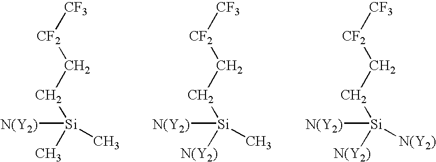
- hydrofluorocarbon pendants attached to the silicon atom can be varied.
- aminosilane precursors with alternative hydrofluorocarbon pendants are:
- Z is a hydrofluorocarbon pendant that can be straight or branched and wherein the Z pendants can be different. There can be up to 3 hydrofluorocarbon pendants.
- the other non-hydrofluorocarbon pendants attached to the silicon atom can be hydrogens or hydrocarbons with at least one reactive amine pendant.
- hydrofluorocarbon pendants examples are:
- the hydrofluorocarbon pendant can be straight or branched as shown above.
- the integer n is typically from 0 to 16 and the integer m is typically from 2 to 19.
- the group J can be another hydrocarbon, fluorocarbon or hydrofluorocarbon and the J groups can be different.
- the group K can be another hydrocarbon or hydrofluorocarbon. Branching groups can be attached to one or more of the carbons on the hydrofluorocarbon pendants. Examples of J and K include the following groups, but are not limited to these:
- the fluorocarbon group shown above can be attached at site J.
- the integer m can be a number from 0 to 18 and n can be an integer from 0 to 18.
- the number of silicon atoms can also be varied.
- Examples of amino-functionalized silane and siloxane precursors with alternative number of silicon atoms are:
- P can be an amine, hydrogen, a hydrocarbon, or a hydrofluorocarbon pendant and wherein the pendants can be different.
- the integer m can be 1, 2, or 3 and the integer n can be 1 to 8.
- At least one reactive amine pendant can be attached to a silicon atom.
- the amino-functionalized silane precursor can also be a cyclic aminosilane, and wherein two of the amine functions are incorporated into the ring.
- cyclic aminosilanes are:
- Y is hydrogen or hydrocarbon.
- the number of carbons between nitrogen atoms is a minimum of two.
- the integer n is typically 1 to 4.
- the cyclic aminosilanes can also have a variable number and type of pendant attached to the silicon atom.
- the other pendants attached to the silicon aside from the cyclic group can be hydrogen, an amine, a hydrocarbon, or a hydrofluorocarbon.
- FIG. 3 shows a single-chamber vacuum system 300 for the chemical vapor deposition of an anti-stiction coating on a MEMS device 310 .
- the MEMS device 310 can comprise a full wafer, parts of a wafer, or an individual die.
- the CVD system 300 can comprise a vacuum chamber 320 , a vacuum pump 322 to evacuate the chamber 320 through exhaust line 324 , a chamber isolation valve 326 to seal the vacuum chamber during coating deposition in the static mode, and a throttle valve 328 to control the chamber pressure and precursor flow rate during coating deposition in the continuous flow mode.
- the MEMS device 310 can be mounted on a chuck 312 .
- the CVD system 300 can further comprise a precursor reservoir 330 containing the amino-functionalized precursor liquid, a precursor variable leak valve 332 to introduce the precursor vapor into the vacuum chamber 320 , and a precursor isolation valve 334 .
- the CVD system 300 can further comprise a means to clean the MEMS device surface.
- the CVD system 300 can include a microwave source 340 for generation of a cleaning plasma, an inlet for oxygen gas 342 , and an inlet for other cleaning gases 344 .
- the flow rate of the oxygen and cleaning gases can be controlled by cleaning gas mass flow controllers 346 and cleaning gas isolation valves 348 .
- the CVD system 300 can also include means (not shown) to control the temperature of the chamber and precursor feed lines to inhibit condensation of precursor.
- the CVD system can be a dual-chamber vacuum system (not shown), comprising a cleaning chamber to pre-clean the surface of the MEMS device 310 and a separate deposition chamber for chemical vapor deposition of the anti-stiction coating.
- the dual chambers can have an intermediate transfer chamber for the transfer of the MEMS device 310 between the cleaning and deposition chambers.
- the dual chamber system can also have a cassette chamber for loading the MEMS device 310 into the transfer chamber.
- the MEMS device 310 have a clean, hydroxylated silicon surface for reaction with the amino-functionalized silane precursor.
- These residues can prevent adhesion of the coating to the surface of the MEMS device 310 or combine with the precursor material to form reaction products that cause additional stiction.
- liquids can be vacuumed out of the narrow channels at low pressure and cause MEMS components to adhere together. While supercritical drying processes can effectively eliminate solvents, these drying processes may leave the MEMS device surface terminated with methanol or other organic compounds unsuitable for reaction with the aminosilane precursor. Additionally, small amounts of residual organic compounds or surface terminations can react with the coating precursor and cause adhesion of parts.
- the silicon surface of the MEMS device 310 can be cleaned prior to deposition of the anti-stiction coating.
- a variety of methods can be used to clean the surface, depending on the residual or surface termination left by the fabrication of the MEMS device 310 . These cleaning methods include heating the MEMS device 310 at ambient pressure to a temperature greater than 100° C. in an inert environment, heating the MEMS device 310 at sub-ambient pressure and less than 100° C. in an inert environment, placing the MEMS device 310 in a dry environment for a period of time, cleaning surface residuals with a vapor-phase ozone system, and cleaning the surface with an oxidizing plasma.
- Downstream plasma cleaning with an oxidizing plasma is an effective method to remove organic residues left on the surface of MEMS device 310 after supercritical drying.
- the organic residues can be removed from the surface by downstream plasma cleaning without affecting the mechanical functioning of the MEMS device 310 .
- the surface can be thoroughly cleaned while leaving it terminated with silanol groups that are preferred for good adhesion of the anti-stiction coating.
- a mixture of oxygen and hydrogen with some percentage of an inert gas i.e., argon, nitrogen, or helium
- the mass flow of the cleaning gases, vacuum chamber pressure, and plasma power can be controlled to create the proper surface condition for obtaining well controlled, hydrophobic coatings.
- Oxide growth can be controlled by including a small amount of reducing gas, such as hydrogen, in the cleaning gas mixture.
- a ratio of between one and twenty percent of hydrogen to oxygen adds enough of a reducing gas to the mixture to control oxide growth and properly condition the silicon surface for coating deposition.
- the cleaning gas mixture can be diluted with up to about 80% of an inert gas for safety reasons, to control oxide formation, and aid in surface preparation. With this cleaning gas mixture, amino-functionalized silane precursors can deposit at higher surface densities than with other plasma cleaning gases that contain only nitrogen, oxygen and/or an inert gas.
- the amino-functionalized silane precursor can be reacted with the surface silanol groups to form the anti-stiction coating.
- Amino-functionalized silane precursors react directly with surface groups allowing bond formation without the addition of water or subsequent heating.
- the rate of a S N 2 reaction that occurs at the silicon surface between precursor and surface terminal groups is primarily a function of leaving group type. Film deposition is possible in either of two modes: static or continuous flow of precursor into the chamber. This fast reaction of aminosilanes with the silicon surface enables the use of either mode of processing.
- the deposition chamber 320 can be evacuated with vacuum pump 322 and then gated off with chamber isolation valve 326 while the precursor isolation valve 334 to the precursor reservoir 330 containing the precursor liquid is left open.
- the precursor leak valve 332 can be adjusted manually to optimize for precursor volatility. The precursor vapor is thereby permitted to leak into the gated-off vacuum chamber 310 and the chamber pressure eventually rises to the vapor pressure of the precursor liquid when the surface coverage is complete.
- the precursor vapor is continuously pumped through the chamber 320 at a low pressure that is controlled by the throttle valve 328 .
- Previous, slower reacting, chlorosilanes and hydroxysilanes deposit very poorly when using the continuous flow mode.
- the amino-functionalized silane precursors provide equivalent or superior films in the continuous flow mode due to their higher reactivity and improved coverage.
- the amount of ambient leakage into the deposition chamber 320 and the amount of material sorption on or in the chamber walls can be important in the CVD process. Stray vaporous species will dilute the concentration of the precursor and reduce reaction rates and film density. A well-sealed chamber 320 and heating of the chamber and feed line surfaces that come into contact with the precursor can help to prevent this contamination problem.
- the temperature of the MEMS device 310 during deposition can be maintained at a temperature below that of the surrounding chamber surfaces and near or just slightly above the temperature of the precursor reservoir 330 . Heating feed lines and chamber walls also helps to minimize unwanted condensation of precursor. The temperature of these surfaces can be maintained well above the temperature of the precursor reservoir 330 (e.g., a differential temperature of about 30–50° C.).
- the rate of film growth on the surface of the MEMS device 310 is a function of precursor reactivity and the partial pressure of the precursor in the deposition chamber 320 .
- Precursors that have a low ambient vapor pressure must be heated to elevated temperature to provide dense monolayer films in a reasonable time. If the molecule boils at a very high temperature (e.g., above 220° C. at 1 atm.), condensation of the precursor on cold spots in the vacuum chamber 320 may be observed even if surfaces are heated.
- a very high temperature e.g., above 220° C. at 1 atm.
- condensation of the precursor on cold spots in the vacuum chamber 320 may be observed even if surfaces are heated.
- unbranched fluorocarbon precursors it may be difficult to deposit dense films if the material has a molecular weight greater than 600 g/mol.
- Amino-functionalized silane precursors can react quickly with a variety of surfaces and organic molecules. If the precursor is permitted to react with the surface of the MEMS device 310 before it is thoroughly cleaned, the resulting reaction product can cause additional stiction and decrease device yield. To prevent this from happening, the cleaning and precursor reaction steps can be performed in separate chambers in a dual chamber vacuum system. Although not essential, separation of the cleaning and the reaction steps generally increases the device yield by reducing contaminant reaction with the precursor before the cleaning step is performed. Also, to prevent contamination of a common transfer chamber, the deposition chamber can be purged with an inert gas while the MEMS device 310 is still in the deposition chamber. The MEMS device 310 can then be removed from the deposition chamber and the chamber cleaned with a plasma to destroy any residual precursor. This method is usually effective for minimizing build-up of the precursor in areas that can foul the MEMS device 310 and reduce product yield.
- a (tridecafluor-1,1,2,2-tetrahydrooctyl)-tris(dimethylamino) silane precursor was used to vapor deposit an anti-stiction coating on a silicon-based MEMS device 310 in a dual-chamber vacuum system.
- the dual-chamber vacuum system comprised a cleaning chamber to pre-clean the surface of the MEMS device 310 and a separate deposition chamber to deposit the anti-stiction coating.
- the MEMS device 310 was placed into the vacuum system in a cassette.
- the vacuum system was pumped down slowly to about 500 millitorr.
- the MEMS device 310 was transferred into the cleaning chamber 320 and placed on a chuck 312 that was heated to 55° C. Downstream plasma cleaning was performed with a oxidizing plasma generated by a microwave source 340 that was adjusted to maximize the number of silanol surface species, while still providing adequate removal of organic contaminants.
- the cleaning gas isolation valves 348 were opened and oxygen gas was introduced through inlet 342 and nitrogen/hydrogen forming gas was introduced through inlet 344 . Flow rate of the oxygen and forming gases were controlled by cleaning gas mass flow controllers 346 . Chamber pressure was controlled by throttle valve 328 .
- Optimized plasma conditions were obtained at a microwave power of 1000 watts, a flow rate of 980 sccm of nitrogen/5.5% hydrogen forming gas, and 600 sccm of oxygen at a chamber pressure of 2800 millitorr. This formulation produced a hydrogen/oxygen ratio of about 8.25%.
- the MEMS device 310 was cleaned in the microwave plasma for one minute in the cleaning chamber and then transferred to the deposition chamber through a common transfer chamber.
- the (tridecafluor-1,1,2,2-tetrahydrooctyl)-tris(dimethylamino) silane precursor was deposited on the cleaned silicon surface of the MEMS device 310 in the continuous flow mode.
- the MEMS device 310 was placed on a chuck 312 that was heated to 35° C. in the deposition chamber 320 .
- the precursor reservoir 330 containing the precursor liquid was also heated to a temperature of 35° C.
- the feed lines connecting the precursor reservoir 330 to the deposition chamber 320 were heated to 85° C.
- the walls and other parts of the deposition chamber 320 were heated to about 60 to 70° C. After evacuation of the deposition chamber 320 by vacuum pump 322 , precursor vapor was introduced into the chamber 320 by opening precursor isolation valve 334 .
- Precursor pressure was controlled by means of precursor variable leak valve 332 and throttle valve 328 .
- the MEMS device 310 was exposed to the precursor vapor for 12.5 minutes while maintaining a precursor pressure of 2 to 10 millitorr in the deposition chamber 320 .
- the precursor isolation valve 334 was closed and the deposition chamber 320 was purged with 200 sccm nitrogen at 500 millitorr for two minutes.
- the coated MEMS device 310 was then returned to the common transfer chamber and the deposition chamber was then cleaned with a nitrogen plasma to prevent fouling of the vacuum system with any stray precursor.
- the coated MEMS device 310 was then returned to the cassette chamber and cassette chamber was vented slowly to atmosphere for removal of the coated MEMS device 310 .
- a plurality of polysilicon microengines where manufactured to compare the yield of functioning parts coated with a vapor-deposited amino-functionalized precursor with a chlorosilane-based SAM deposited from nonaqueous solution. Both the amino-functionalized precursor and the chlorosilane precursor had the same (hexadecafluoro-1,1,2,2-tetrahydodecyl) hydrophobic tail group.
- the polysilicon microengines were released by an HF etch and dried with supercritical carbon dioxide. The released and dried microengines were then coated with the amino-functionalized precursor according to the above-described CVD method or coated with the liquid-phase SAM. The yield of functioning microengines with vapor-deposited coatings was 25% higher than for those coated with liquid-phase SAMs.
- the contact angle of silicon substrates coated with the amino-functionalized precursors was between 103 and 106 degrees, suggesting that a dense monolayer coating was formed by the CVD method.
- atomic force micrographs (AFM) of the vapor-deposited coatings indicated a smooth surface, with no apparent change in roughness from a bare silicon surface.
- surfaces coated with the liquid-phase SAM showed the presence of aggregated coating material and additional aggregate formation upon exposure to humidity. This aggregate formation is thought to be due to the sensitivity of the chlorosilane precursors to moisture and apparently accounts for the lower yield of functioning microengines coated with liquid-phase SAMs.
Landscapes
- Chemical & Material Sciences (AREA)
- Engineering & Computer Science (AREA)
- Nanotechnology (AREA)
- Materials Engineering (AREA)
- Physics & Mathematics (AREA)
- Metallurgy (AREA)
- General Physics & Mathematics (AREA)
- Mechanical Engineering (AREA)
- General Chemical & Material Sciences (AREA)
- Organic Chemistry (AREA)
- Crystallography & Structural Chemistry (AREA)
- Condensed Matter Physics & Semiconductors (AREA)
- Chemical Kinetics & Catalysis (AREA)
- Composite Materials (AREA)
- Plasma & Fusion (AREA)
- Manufacturing & Machinery (AREA)
- Inorganic Chemistry (AREA)
- Micromachines (AREA)
- Chemical Vapour Deposition (AREA)
Abstract
Description

where X is a hydrocarbon pendant that can be straight or branched and can comprise alkyl or aryl groups. There can be up to 3 hydrocarbon pendants attached to the silicon atom. The non-hydrocarbon pendants can be hydrogens or hydrofluorocarbons and at least one reactive amine pendant. The following are some examples of hydrocarbon pendants, although other hydrocarbon pendants are also suitable for the present invention:

where n is an integer generally from 1 to 20.
where Y is an amine hydrogen or alkyl- or aryl-hydrocarbon and wherein the Y groups can be different. There can be 1 to 3 amine pendants attached to the silicon atom. The other non-amine pendants attached to the silicon atom can be hydrogens, hydrocarbons, or hydrofluorocarbons. The following are examples of suitable Y groups attached to the amino nitrogen atom, although Y is not limited to these:


where Z is a hydrofluorocarbon pendant that can be straight or branched and wherein the Z pendants can be different. There can be up to 3 hydrofluorocarbon pendants. The other non-hydrofluorocarbon pendants attached to the silicon atom can be hydrogens or hydrocarbons with at least one reactive amine pendant.

The hydrofluorocarbon pendant can be straight or branched as shown above. The integer n is typically from 0 to 16 and the integer m is typically from 2 to 19. The group J can be another hydrocarbon, fluorocarbon or hydrofluorocarbon and the J groups can be different. The group K can be another hydrocarbon or hydrofluorocarbon. Branching groups can be attached to one or more of the carbons on the hydrofluorocarbon pendants. Examples of J and K include the following groups, but are not limited to these:

The fluorocarbon group shown above can be attached at site J. The integer m can be a number from 0 to 18 and n can be an integer from 0 to 18.

where P can be an amine, hydrogen, a hydrocarbon, or a hydrofluorocarbon pendant and wherein the pendants can be different. The integer m can be 1, 2, or 3 and the integer n can be 1 to 8. At least one reactive amine pendant can be attached to a silicon atom.

where Y is hydrogen or hydrocarbon. The number of carbons between nitrogen atoms is a minimum of two. The integer n is typically 1 to 4. The cyclic aminosilanes can also have a variable number and type of pendant attached to the silicon atom. The other pendants attached to the silicon aside from the cyclic group can be hydrogen, an amine, a hydrocarbon, or a hydrofluorocarbon.
Claims (21)
Priority Applications (1)
| Application Number | Priority Date | Filing Date | Title |
|---|---|---|---|
| US10/115,411 US7045170B1 (en) | 2002-04-03 | 2002-04-03 | Anti-stiction coating for microelectromechanical devices |
Applications Claiming Priority (1)
| Application Number | Priority Date | Filing Date | Title |
|---|---|---|---|
| US10/115,411 US7045170B1 (en) | 2002-04-03 | 2002-04-03 | Anti-stiction coating for microelectromechanical devices |
Publications (1)
| Publication Number | Publication Date |
|---|---|
| US7045170B1 true US7045170B1 (en) | 2006-05-16 |
Family
ID=36318068
Family Applications (1)
| Application Number | Title | Priority Date | Filing Date |
|---|---|---|---|
| US10/115,411 Expired - Lifetime US7045170B1 (en) | 2002-04-03 | 2002-04-03 | Anti-stiction coating for microelectromechanical devices |
Country Status (1)
| Country | Link |
|---|---|
| US (1) | US7045170B1 (en) |
Cited By (25)
| Publication number | Priority date | Publication date | Assignee | Title |
|---|---|---|---|---|
| US20030188682A1 (en) * | 1999-12-03 | 2003-10-09 | Asm Microchemistry Oy | Method of growing oxide films |
| US20050106774A1 (en) * | 2003-11-13 | 2005-05-19 | Dmitri Simonian | Surface processes in fabrications of microstructures |
| US20060115594A1 (en) * | 2003-09-05 | 2006-06-01 | Moffat William A | Apparatus for the efficient coating of substrates including plasma cleaning |
| US20060121197A1 (en) * | 2003-09-05 | 2006-06-08 | Moffat William A | Method for silane coating of indium tin oxide surfaced substrates |
| US20080020593A1 (en) * | 2006-07-21 | 2008-01-24 | Wang Chang-Gong | ALD of metal silicate films |
| US20080055703A1 (en) * | 2006-06-28 | 2008-03-06 | Pan Shaoher X | In situ application of anti-stiction materials to micro devices |
| US20080074771A1 (en) * | 2006-09-25 | 2008-03-27 | Paul Felice Reboa | Method for providing an anti-stiction coating on a metal surface |
| US20080108163A1 (en) * | 2006-10-02 | 2008-05-08 | Chien-Hua Chen | Microelectromechanical system device and method for preparing the same for subsequent processing |
| US20080116554A1 (en) * | 2006-11-21 | 2008-05-22 | Spatial Photonics, Inc. | Packaging micro devices |
| US20090209081A1 (en) * | 2007-12-21 | 2009-08-20 | Asm International N.V. | Silicon Dioxide Thin Films by ALD |
| US20090231667A1 (en) * | 2007-05-03 | 2009-09-17 | Yoshihiro Maeda | Mirror device with an anti-stiction layer |
| US20100203260A1 (en) * | 2003-09-05 | 2010-08-12 | Moffat William A | Method for efficient coating of substrates including plasma cleaning and dehydration |
| US20100242258A1 (en) * | 2001-06-30 | 2010-09-30 | Texas Instruments Incorporated | Lubricating Micro-Machined Devices Using Fluorosurfactants |
| US20110198736A1 (en) * | 2010-02-17 | 2011-08-18 | Asm America, Inc. | Reactive site deactivation against vapor deposition |
| US20130032904A1 (en) * | 2011-08-04 | 2013-02-07 | Robert Bosch Gmbh | Coated Capacitive Sensor |
| US9223203B2 (en) | 2011-07-08 | 2015-12-29 | Asm International N.V. | Microcontact printed films as an activation layer for selective atomic layer deposition |
| CN107644808A (en) * | 2016-07-21 | 2018-01-30 | 东京毅力科创株式会社 | The back side friction of substrate reduces |
| US10183856B2 (en) | 2017-01-16 | 2019-01-22 | Sensortek Technology Corp. | Manufacturing method of micro-electro-mechanical systems device |
| WO2019108377A1 (en) * | 2017-11-29 | 2019-06-06 | Tokyo Electron Limited | Back-side friction reduction of a substrate |
| US10504715B2 (en) | 2016-07-21 | 2019-12-10 | Tokyo Electron Limited | Back-side friction reduction of a substrate |
| CN111570216A (en) * | 2020-04-27 | 2020-08-25 | 江苏菲沃泰纳米科技有限公司 | Composite protective film layer with silane transition layer and preparation method and product thereof |
| CN112267105A (en) * | 2020-09-30 | 2021-01-26 | 中国科学院上海微系统与信息技术研究所 | Single-cavity PECVD deposition process for producing silicon heterojunction solar cell |
| US11203702B1 (en) | 2019-10-17 | 2021-12-21 | National Technology & Engineering Solutions Of Sandia, Llc | Functionalized coating polymers and uses thereof |
| US20210398846A1 (en) * | 2020-06-17 | 2021-12-23 | Tokyo Electron Limited | Method for area selective deposition using a surface cleaning process |
| US12024770B2 (en) * | 2018-08-10 | 2024-07-02 | Applied Materials, Inc. | Methods for selective deposition using self-assembled monolayers |
Citations (12)
| Publication number | Priority date | Publication date | Assignee | Title |
|---|---|---|---|---|
| US3903052A (en) * | 1972-09-06 | 1975-09-02 | Bayer Ag | Polymers containing alkoxysilyl-substituted biuret groups and processes for their preparation |
| US4529659A (en) * | 1983-11-05 | 1985-07-16 | Nippon Telegraph & Telephone Public Corporation | Magnetic recording member and process for manufacturing the same |
| US4671933A (en) * | 1985-06-24 | 1987-06-09 | Stauffer-Wacker Silicones Corporation | Method for inhibiting corrosion of metal surfaces |
| US4795622A (en) * | 1986-04-24 | 1989-01-03 | Toa Nenryo Kogyo Kabushiki Kaisha | Method for producing silicon-imide |
| US5128416A (en) * | 1988-05-02 | 1992-07-07 | Sumitomo Chemical Company, Limited | Modified diene polymer rubbers |
| US5542295A (en) | 1994-12-01 | 1996-08-06 | Analog Devices, Inc. | Apparatus to minimize stiction in micromachined structures |
| JPH08325274A (en) | 1995-05-26 | 1996-12-10 | Shin Etsu Chem Co Ltd | Organosilicon compound, its production and surface-treating agent |
| US5822170A (en) | 1997-10-09 | 1998-10-13 | Honeywell Inc. | Hydrophobic coating for reducing humidity effect in electrostatic actuators |
| US6114044A (en) | 1997-05-30 | 2000-09-05 | Regents Of The University Of California | Method of drying passivated micromachines by dewetting from a liquid-based process |
| US6391803B1 (en) * | 2001-06-20 | 2002-05-21 | Samsung Electronics Co., Ltd. | Method of forming silicon containing thin films by atomic layer deposition utilizing trisdimethylaminosilane |
| US20030036085A1 (en) * | 2002-08-19 | 2003-02-20 | Salinaro Richard F | Membranes |
| US6576489B2 (en) * | 2001-05-07 | 2003-06-10 | Applied Materials, Inc. | Methods of forming microstructure devices |
-
2002
- 2002-04-03 US US10/115,411 patent/US7045170B1/en not_active Expired - Lifetime
Patent Citations (12)
| Publication number | Priority date | Publication date | Assignee | Title |
|---|---|---|---|---|
| US3903052A (en) * | 1972-09-06 | 1975-09-02 | Bayer Ag | Polymers containing alkoxysilyl-substituted biuret groups and processes for their preparation |
| US4529659A (en) * | 1983-11-05 | 1985-07-16 | Nippon Telegraph & Telephone Public Corporation | Magnetic recording member and process for manufacturing the same |
| US4671933A (en) * | 1985-06-24 | 1987-06-09 | Stauffer-Wacker Silicones Corporation | Method for inhibiting corrosion of metal surfaces |
| US4795622A (en) * | 1986-04-24 | 1989-01-03 | Toa Nenryo Kogyo Kabushiki Kaisha | Method for producing silicon-imide |
| US5128416A (en) * | 1988-05-02 | 1992-07-07 | Sumitomo Chemical Company, Limited | Modified diene polymer rubbers |
| US5542295A (en) | 1994-12-01 | 1996-08-06 | Analog Devices, Inc. | Apparatus to minimize stiction in micromachined structures |
| JPH08325274A (en) | 1995-05-26 | 1996-12-10 | Shin Etsu Chem Co Ltd | Organosilicon compound, its production and surface-treating agent |
| US6114044A (en) | 1997-05-30 | 2000-09-05 | Regents Of The University Of California | Method of drying passivated micromachines by dewetting from a liquid-based process |
| US5822170A (en) | 1997-10-09 | 1998-10-13 | Honeywell Inc. | Hydrophobic coating for reducing humidity effect in electrostatic actuators |
| US6576489B2 (en) * | 2001-05-07 | 2003-06-10 | Applied Materials, Inc. | Methods of forming microstructure devices |
| US6391803B1 (en) * | 2001-06-20 | 2002-05-21 | Samsung Electronics Co., Ltd. | Method of forming silicon containing thin films by atomic layer deposition utilizing trisdimethylaminosilane |
| US20030036085A1 (en) * | 2002-08-19 | 2003-02-20 | Salinaro Richard F | Membranes |
Non-Patent Citations (4)
| Title |
|---|
| Bunker, et al., "The Impact of Solution Agglomeration on the Deposition of Self-Assembled Monolayers," Langmuir 20, 7742 (2000). |
| de Boer, et al., "Tribology of MEMS," MRS Bulletin, Apr. 2001, pp. 302-304. |
| Maboudin, Roya, "Surface processes in MEMS technology," Surface Science Reports 30, 207 (1998). |
| Mayer, et al., "Chemical Vapor Deposition of Fluoroalkylsilane Monolayer Films for Adhesion Control in Microelectromechanical Systems," J. Vac. Sci. Technol. B18, 2433 (2000). |
Cited By (53)
| Publication number | Priority date | Publication date | Assignee | Title |
|---|---|---|---|---|
| US7824492B2 (en) | 1999-12-03 | 2010-11-02 | Asm International N.V. | Method of growing oxide thin films |
| US20040065253A1 (en) * | 1999-12-03 | 2004-04-08 | Eva Tois | Method of growing oxide thin films |
| US7771533B2 (en) * | 1999-12-03 | 2010-08-10 | Asm International N.V. | Atomic-layer-chemical-vapor-deposition of films that contain silicon dioxide |
| US9514956B2 (en) | 1999-12-03 | 2016-12-06 | Asm International N.V. | Method of growing oxide thin films |
| US7771534B2 (en) | 1999-12-03 | 2010-08-10 | Asm International N.V. | Method of growing oxide thin films |
| US20070163488A1 (en) * | 1999-12-03 | 2007-07-19 | Eva Tois | Method of growing oxide thin films |
| US20030188682A1 (en) * | 1999-12-03 | 2003-10-09 | Asm Microchemistry Oy | Method of growing oxide films |
| US20110104906A1 (en) * | 1999-12-03 | 2011-05-05 | Asm International N.V. | Method of growing oxide thin films |
| US8049946B2 (en) * | 2001-06-30 | 2011-11-01 | Texas Instruments Incorporated | Lubricating micro-machined devices using fluorosurfactants |
| US20100242258A1 (en) * | 2001-06-30 | 2010-09-30 | Texas Instruments Incorporated | Lubricating Micro-Machined Devices Using Fluorosurfactants |
| US20060121197A1 (en) * | 2003-09-05 | 2006-06-08 | Moffat William A | Method for silane coating of indium tin oxide surfaced substrates |
| US20130000557A1 (en) * | 2003-09-05 | 2013-01-03 | Moffat William A | Apparatus for the Efficient Coating of Subtrates Including Plasma Cleaning |
| US8252375B2 (en) * | 2003-09-05 | 2012-08-28 | Yield Engineering Systems, Inc. | Apparatus for the efficient coating of substrates including plasma cleaning |
| US20060115594A1 (en) * | 2003-09-05 | 2006-06-01 | Moffat William A | Apparatus for the efficient coating of substrates including plasma cleaning |
| US8361548B2 (en) * | 2003-09-05 | 2013-01-29 | Yield Engineering Systems, Inc. | Method for efficient coating of substrates including plasma cleaning and dehydration |
| US20100203260A1 (en) * | 2003-09-05 | 2010-08-12 | Moffat William A | Method for efficient coating of substrates including plasma cleaning and dehydration |
| US20050106774A1 (en) * | 2003-11-13 | 2005-05-19 | Dmitri Simonian | Surface processes in fabrications of microstructures |
| US7468830B2 (en) * | 2006-06-28 | 2008-12-23 | Spatial Photonics, Inc. | In SITU application of anti-stiction materials to micro devices |
| US20080055703A1 (en) * | 2006-06-28 | 2008-03-06 | Pan Shaoher X | In situ application of anti-stiction materials to micro devices |
| US7795160B2 (en) | 2006-07-21 | 2010-09-14 | Asm America Inc. | ALD of metal silicate films |
| US20080020593A1 (en) * | 2006-07-21 | 2008-01-24 | Wang Chang-Gong | ALD of metal silicate films |
| US7618682B2 (en) | 2006-09-25 | 2009-11-17 | Hewlett-Packard Development Company, L.P. | Method for providing an anti-stiction coating on a metal surface |
| US20080074771A1 (en) * | 2006-09-25 | 2008-03-27 | Paul Felice Reboa | Method for providing an anti-stiction coating on a metal surface |
| US7443001B2 (en) | 2006-10-02 | 2008-10-28 | Helwett-Packard Development Company, L.P. | Preparation of microelectromechanical system device using an anti-stiction material and selective plasma sputtering |
| US20080108163A1 (en) * | 2006-10-02 | 2008-05-08 | Chien-Hua Chen | Microelectromechanical system device and method for preparing the same for subsequent processing |
| US20080116554A1 (en) * | 2006-11-21 | 2008-05-22 | Spatial Photonics, Inc. | Packaging micro devices |
| CN101221911B (en) * | 2006-11-21 | 2011-07-20 | 视频有限公司 | Packaging micro devices |
| US7944600B2 (en) | 2007-05-03 | 2011-05-17 | Silicon Quest Kabushiki-Kaisha | Mirror device with an anti-stiction layer |
| US20110058247A1 (en) * | 2007-05-03 | 2011-03-10 | Yoshihiro Maeda | Mirror device with an anti-stiction layer |
| US20090231667A1 (en) * | 2007-05-03 | 2009-09-17 | Yoshihiro Maeda | Mirror device with an anti-stiction layer |
| US8134772B2 (en) | 2007-05-03 | 2012-03-13 | Silicon Quest Kabushiki-Kaisha | Mirror device with an anti-stiction layer |
| US7880952B2 (en) | 2007-05-03 | 2011-02-01 | Silicon Quest Kabushiki-Kaisha | Mirror device with an anti-stiction layer |
| US20090209081A1 (en) * | 2007-12-21 | 2009-08-20 | Asm International N.V. | Silicon Dioxide Thin Films by ALD |
| US8501637B2 (en) | 2007-12-21 | 2013-08-06 | Asm International N.V. | Silicon dioxide thin films by ALD |
| WO2011103062A2 (en) * | 2010-02-17 | 2011-08-25 | Asm America, Inc. | Reactive site deactivation against vapor deposition |
| WO2011103062A3 (en) * | 2010-02-17 | 2012-04-05 | Asm America, Inc. | Reactive site deactivation against vapor deposition |
| US20110198736A1 (en) * | 2010-02-17 | 2011-08-18 | Asm America, Inc. | Reactive site deactivation against vapor deposition |
| US8293658B2 (en) | 2010-02-17 | 2012-10-23 | Asm America, Inc. | Reactive site deactivation against vapor deposition |
| KR101496644B1 (en) | 2010-02-17 | 2015-02-27 | 에이에스엠 아메리카, 인코포레이티드 | Reactive site deactivation against vapor deposition |
| US9223203B2 (en) | 2011-07-08 | 2015-12-29 | Asm International N.V. | Microcontact printed films as an activation layer for selective atomic layer deposition |
| US20130032904A1 (en) * | 2011-08-04 | 2013-02-07 | Robert Bosch Gmbh | Coated Capacitive Sensor |
| CN107644808A (en) * | 2016-07-21 | 2018-01-30 | 东京毅力科创株式会社 | The back side friction of substrate reduces |
| US10784100B2 (en) | 2016-07-21 | 2020-09-22 | Tokyo Electron Limited | Back-side friction reduction of a substrate |
| US10504715B2 (en) | 2016-07-21 | 2019-12-10 | Tokyo Electron Limited | Back-side friction reduction of a substrate |
| CN107644808B (en) * | 2016-07-21 | 2023-08-22 | 东京毅力科创株式会社 | Substrate, method of processing substrate, and processing chamber system |
| US10183856B2 (en) | 2017-01-16 | 2019-01-22 | Sensortek Technology Corp. | Manufacturing method of micro-electro-mechanical systems device |
| WO2019108377A1 (en) * | 2017-11-29 | 2019-06-06 | Tokyo Electron Limited | Back-side friction reduction of a substrate |
| US12024770B2 (en) * | 2018-08-10 | 2024-07-02 | Applied Materials, Inc. | Methods for selective deposition using self-assembled monolayers |
| US11203702B1 (en) | 2019-10-17 | 2021-12-21 | National Technology & Engineering Solutions Of Sandia, Llc | Functionalized coating polymers and uses thereof |
| CN111570216A (en) * | 2020-04-27 | 2020-08-25 | 江苏菲沃泰纳米科技有限公司 | Composite protective film layer with silane transition layer and preparation method and product thereof |
| CN111570216B (en) * | 2020-04-27 | 2023-10-13 | 江苏菲沃泰纳米科技股份有限公司 | Composite protective film layer with silane transition layer, preparation method thereof and product |
| US20210398846A1 (en) * | 2020-06-17 | 2021-12-23 | Tokyo Electron Limited | Method for area selective deposition using a surface cleaning process |
| CN112267105A (en) * | 2020-09-30 | 2021-01-26 | 中国科学院上海微系统与信息技术研究所 | Single-cavity PECVD deposition process for producing silicon heterojunction solar cell |
Similar Documents
| Publication | Publication Date | Title |
|---|---|---|
| US7045170B1 (en) | Anti-stiction coating for microelectromechanical devices | |
| US10900123B2 (en) | Apparatus and method for controlled application of reactive vapors to produce thin films and coatings | |
| US7413774B2 (en) | Method for controlled application of reactive vapors to produce thin films and coatings | |
| KR100762573B1 (en) | Controlled vapor deposition of multilayered coating adhered by an oxide layer | |
| US6576489B2 (en) | Methods of forming microstructure devices | |
| US8298614B2 (en) | Method of depositing a multilayer coating with a variety of oxide adhesion layers and organic layers | |
| KR101827020B1 (en) | Method of reducing pattern collapse in high aspect ratio nanostructures | |
| US8987029B2 (en) | Protective thin films for use during fabrication of semiconductors, MEMS, and microstructures | |
| US20140308822A1 (en) | Deposition technique for depositing a coating on a device | |
| KR20210003966A (en) | Chemical delivery chamber for self-assembled monolayer processes | |
| Herrmann et al. | Conformal hydrophobic coatings prepared using atomic layer deposition seed layers and non-chlorinated hydrophobic precursors | |
| KR100697505B1 (en) | Apparatus and method for controlled application of reactive vapors to produce thin films and coatings | |
| JP3331957B2 (en) | Surface treatment method for structure to be treated | |
| KR100812182B1 (en) | Vapor deposition of self-assembled monolayers for functionalization of surface in nanoimprint lithography | |
| Kobrin et al. | Molecular vapor deposition (MVD) for improved SAM coatings | |
| Kobrin et al. | Durable Anti-Stiction Coatings by Molecular Vapor Deposition (MVD) | |
| TW202433550A (en) | Method of blocking dielectric surfaces using blocking molecules to enable selective epi deposition | |
| KR20050057806A (en) | Method for fabricating self-assembled monolayers in the gas phase |
Legal Events
| Date | Code | Title | Description |
|---|---|---|---|
| AS | Assignment |
Owner name: SANDIA CORPORATION, NEW MEXICO Free format text: ASSIGNMENT OF ASSIGNORS INTEREST;ASSIGNORS:HANKINS, MATTHEW G.;MAYER, THOMAS M.;WHEELER, DAVID R.;REEL/FRAME:013148/0735;SIGNING DATES FROM 20020401 TO 20020402 |
|
| AS | Assignment |
Owner name: ENERGY, U.S. DEPARTMENT OF, DISTRICT OF COLUMBIA Free format text: CONFIRMATORY LICENSE;ASSIGNOR:SANDIA CORPORATION;REEL/FRAME:013628/0789 Effective date: 20020630 |
|
| STCF | Information on status: patent grant |
Free format text: PATENTED CASE |
|
| FPAY | Fee payment |
Year of fee payment: 4 |
|
| FPAY | Fee payment |
Year of fee payment: 8 |
|
| AS | Assignment |
Owner name: NATIONAL TECHNOLOGY & ENGINEERING SOLUTIONS OF SAN Free format text: CHANGE OF NAME;ASSIGNOR:SANDIA CORPORATION;REEL/FRAME:043696/0143 Effective date: 20170501 |
|
| MAFP | Maintenance fee payment |
Free format text: PAYMENT OF MAINTENANCE FEE, 12TH YEAR, LARGE ENTITY (ORIGINAL EVENT CODE: M1553) Year of fee payment: 12 |