US7041964B2 - Method and apparatus for improved collection efficiency of speckle based navigation sensors using lightpipes and reflectors - Google Patents
Method and apparatus for improved collection efficiency of speckle based navigation sensors using lightpipes and reflectors Download PDFInfo
- Publication number
- US7041964B2 US7041964B2 US10/632,619 US63261903A US7041964B2 US 7041964 B2 US7041964 B2 US 7041964B2 US 63261903 A US63261903 A US 63261903A US 7041964 B2 US7041964 B2 US 7041964B2
- Authority
- US
- United States
- Prior art keywords
- lightpipe
- face
- speckle
- pair
- elliptical
- Prior art date
- Legal status (The legal status is an assumption and is not a legal conclusion. Google has not performed a legal analysis and makes no representation as to the accuracy of the status listed.)
- Expired - Lifetime, expires
Links
Images


Classifications
-
- H—ELECTRICITY
- H10—SEMICONDUCTOR DEVICES; ELECTRIC SOLID-STATE DEVICES NOT OTHERWISE PROVIDED FOR
- H10F—INORGANIC SEMICONDUCTOR DEVICES SENSITIVE TO INFRARED RADIATION, LIGHT, ELECTROMAGNETIC RADIATION OF SHORTER WAVELENGTH OR CORPUSCULAR RADIATION
- H10F55/00—Radiation-sensitive semiconductor devices covered by groups H10F10/00, H10F19/00 or H10F30/00 being structurally associated with electric light sources and electrically or optically coupled thereto
-
- G—PHYSICS
- G01—MEASURING; TESTING
- G01J—MEASUREMENT OF INTENSITY, VELOCITY, SPECTRAL CONTENT, POLARISATION, PHASE OR PULSE CHARACTERISTICS OF INFRARED, VISIBLE OR ULTRAVIOLET LIGHT; COLORIMETRY; RADIATION PYROMETRY
- G01J1/00—Photometry, e.g. photographic exposure meter
- G01J1/02—Details
- G01J1/04—Optical or mechanical part supplementary adjustable parts
- G01J1/0407—Optical elements not provided otherwise, e.g. manifolds, windows, holograms, gratings
- G01J1/0422—Optical elements not provided otherwise, e.g. manifolds, windows, holograms, gratings using light concentrators, collectors or condensers
-
- H—ELECTRICITY
- H10—SEMICONDUCTOR DEVICES; ELECTRIC SOLID-STATE DEVICES NOT OTHERWISE PROVIDED FOR
- H10F—INORGANIC SEMICONDUCTOR DEVICES SENSITIVE TO INFRARED RADIATION, LIGHT, ELECTROMAGNETIC RADIATION OF SHORTER WAVELENGTH OR CORPUSCULAR RADIATION
- H10F30/00—Individual radiation-sensitive semiconductor devices in which radiation controls the flow of current through the devices, e.g. photodetectors
- H10F30/20—Individual radiation-sensitive semiconductor devices in which radiation controls the flow of current through the devices, e.g. photodetectors the devices having potential barriers, e.g. phototransistors
- H10F30/21—Individual radiation-sensitive semiconductor devices in which radiation controls the flow of current through the devices, e.g. photodetectors the devices having potential barriers, e.g. phototransistors the devices being sensitive to infrared, visible or ultraviolet radiation
Definitions
- the invention relates to increasing the light collection efficiency of photodetector arrays using lightpipe or reflector technology.
- Speckle patterns are interference patterns emitted from target surfaces illuminated by coherent light. If the target surface moves, the associated speckle pattern is moved as well. This physical phenomenon provides the basis for speckle based navigation sensors.
- speckle based navigation sensors include a laser light source, optical components and a photodetector.
- the speckle pattern consists of speckle “beams” that are emitted nearly isotropically from the illuminated target surface
- the speckle pattern emitted from an illuminated target surface is made up of quasi-collimated beams of light.
- the cross sectional diameter of an individual speckle beam is inversely proportional to the diameter of the illuminated spot on the target surface and is proportional to the distance from the target surface.
- two photodetector arrays are used in speckle based navigation sensors with each photodetector array sensing motion along one of the axes, respectively.
- the cross sectional speckle beam size must be matched to the size of the individual photodetector array elements.
- the photodetector arrays or collection optics are often positioned at relatively large distances from the target surface and therefore subtend small angles from the target surface. Because speckle “beams” propagate away from the target surface in nearly an isotropic pattern, only a relatively small fraction reaches the photodetector array. This limits the performance of speckle based navigation sensors.
- FIG. 1 shows a conceptual view of a conventional speckle based navigation sensor system for two dimensional navigation.
- Photodetector arrays 120 and 125 detect a fraction of speckle beams 165 from target surface 135 . For example, if photodetector arrays 120 and 125 are located approximately 20 mm from target surface 135 illuminated by the laser light, the angles subtended by photodetector arrays 120 and 125 from target surface 135 are about 7 ⁇ 24 degrees. Because speckle is emitted nearly isotropically only about 1% of the speckle flux strikes photodetector arrays 120 and 125 , assuming a photodector array area of 2.8 ⁇ 8.6 mm.
- lightpipe and reflector technology is used to increase collection efficiency in speckle based navigation sensors.
- Increasing the collection efficiency improves the optical performance of speckle based navigation sensors and also allows reduction in the photodetector size at the price of decreased collection efficiency. Smaller photodetector size typically reduces the photodetector cost.
- FIG. 1 shows prior art speckle based navigation sensor.
- FIG. 2 a shows the use of a lightpipe in accordance with the invention to improve collection efficiency of a speckle based optical navigation sensor.
- FIG. 2 b shows an embodiment of a lightpipe in accordance with the invention where the area of the top face has been increased by slanting it at an angle with respect to the bottom face.
- FIG. 3 shows the use of an elliptical reflector in accordance with the invention to improve collection efficiency of a speckle based optical navigation sensor.
- FIG. 4 shows the effect of undesirable boundary reflections in accordance with the invention.
- FIG. 5 shows the use of a lightpipe in accordance with the invention having elliptical sidewalls to improve collection efficiency of a speckle based optical navigation sensor.
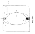
- FIG. 6 shows the use of a lightpipe in accordance with the invention having elliptical sidewalls and microstructure to improve collection efficiency of a speckle based optical navigation sensor.
- FIG. 7 shows a simplified view of a speckle based optical navigation system having improved collection efficiency in accordance with the invention.
- FIG. 2 a shows an embodiment in accordance with the invention.
- Lightpipe 210 is positioned between target surface 235 and photodetector array 220 .
- Lightpipe 210 is made from a transparent material such as, for example, acrylic with a refractive index in the range from about 1.5 to 1.6 or SiO 2 to enhance the refractive index contrast with the surrounding medium, typically air.
- Introduction of lightpipe 210 significantly improves the collection efficiency of speckle beams 265 .
- Photodetector array 220 is positioned directly beneath lightpipe 210 . Speckle beams 265 from target surface 235 strike the top of lightpipe 210 and are refracted into the interior.
- speckle beams 265 propagating away from photodetector array 220 are redirected to strike photodetector array 220 by total internal reflection within lightpipe 210 .
- Sides 202 and 203 of lightpipe 210 are typically absorptive to prevent reversal of the apparent motion of the speckle pattern as described below with reference to FIG. 4 .
- Use of lightpipe 210 allows photodetector array 220 with an area of 0.75 ⁇ 2 mm to collect about 11% of speckle beams 265 compared with larger photodetector array 120 that collects only about 1% of speckle beams 165 .
- FIG. 2 b shows an embodiment in accordance with the invention.
- Lightpipe 250 is similar to lightpipe 210 but top face 275 is inclined at suitable angle with respect to bottom face 265 in FIG. 2 b in order to increase the light gathering area available.
- speckle beams 265 that would not be incident on lightpipe 210 are captured by lightpipe 250 because of the larger surface area of top face 275 .
- FIG. 3 shows an embodiment in accordance with the invention using elliptical reflector 350 to improve the collection efficiency of speckle beams 365 .
- Sidewalls 351 and 352 of elliptical reflector 350 have an elliptical cross-section that is swept in one direction.
- an ellipse has the property that that any light ray passing through one focus of the ellipse is reflected towards the second focus of the ellipse.
- the locus of focal points forms two focal lines; one proximate to the bottom of elliptical sidewalls 351 and 352 and one proximate to top of elliptical sidewalls 351 and 352 in FIG. 3 .
- the locus of focal points is also known as the blur spot.
- speckle beams 365 striking elliptical sidewalls 351 or 352 are reflected to strike photodetector array 320 .
- Typical coatings for elliptical sidewalls are aluminum, silver and gold. Such metallic high reflectivity coatings typically contain a dielectric overcoat to prevent oxidation. High reflectivity dielectric coatings may also be used.
- the collection efficiency using reflector 350 is about 9% which is almost about an order of magnitude better than the conventional embodiment in FIG. 1 .
- the two remaining sidewalls (sidewalls 475 and 480 in FIG. 4 ) of reflector 310 are planar and typically are absorptive. Typically, sidewalls 475 and 480 may be made absorptive by application of a black wax or black tape. Black wax is typically a wax with carbon particulates in it. Alternatively, the two remaining sides of reflector 310 may be open. The reason for this is illustrated in FIG. 4 showing a view of reflector 310 . When speckle beams 365 (see FIG. 3 ) are reflected in a direction predominantly perpendicular to detector elements 410 of photodetector array 320 , the apparent motion of the speckle pattern is reversed.
- speckle pattern 430 The apparent motion of speckle pattern 430 is initially in the direction of sidewall 475 but upon reflection from sidewall 475 , the apparent motion of speckle pattern 430 is reversed and towards sidewall 480 .
- speckle beams 365 reflected in directions predominantly parallel to detector elements 410 of photodetector array 320 provide desirable signals for tracking the apparent motion of speckle patterns.
- Providing planar sidewalls located some distance from photodetector array 320 also reduces the amount of speckle beams 365 (see FIG. 3 ) reflected back to photodetector array 320 from the planar sidewalls.
- FIG. 5 shows lightpipe 500 having elliptical sidewalls 551 and 552 .
- FIG. 5 is similar to FIG. 2 a but has elliptically shaped sidewalls similar to FIG. 3 .
- lightpipe 500 is made from a transparent material such as, for example, acrylic with a refractive index in the range from about 1.5 to 1.6 or SiO 2 .
- Sidewalls 551 and 552 are elliptical and form the interface from the transparent material to air or another material having a different refractive index so that there is a refractive index change along elliptical sidewalls 551 and 552 .
- the planar sidewalls of lightpipe 500 are typically optically absorptive to prevent reversal of the apparent motion of the speckle pattern as described above with reference to FIG. 4 .
- Target surface 535 is typically positioned a small distance away from lightpipe 500 so that most of the speckle beams strike at or near the top focal line of elliptical side walls 551 and 552 in FIG. 5 .
- These speckle beams are then refracted into lightpipe 500 . Speckle beams not refracted towards photodetector array 520 undergo total internal reflection from elliptical sidewalls 551 and 552 and are reflected toward the bottom focal line or blur spot. This increases the collection efficiency on photodetector array 520 to about 11.5%.
- FIG. 6 shows lightpipe 600 having elliptical sidewalls 651 and 652 similar to lightpipe 500 in FIG. 5 but also having microstructure fabricated into lightpipe 600 to further enhance collection efficiency.
- the microstructure is a diffraction grating such as diffraction grating 680 .
- the collection efficiency on photodetector array 620 is improved to about 28%.
- the embodiment in accordance with the invention in FIG. 3 may include a diffraction grating at the top focal line of elliptical sidewalls 351 and 352 opposite photodetector array 320 .
- FIG. 7 shows a simplified view of using a lightpipe in the context of speckle based optical navigation sensor in accordance with the invention.
- Coherent light source 705 is positioned off center with respect to lens 710 so that target surface area 735 may be illuminated.
- lens 710 may be replaced by, for example, a grating without changing the basic operation.
- light beam 755 is directed at an angle towards surface 740 to illuminate target surface area 735 .
- Speckle pattern 780 is scattered into light collector 700 for collection at photodetector array 725 .
- Embodiments of light collector 700 includes any of the embodiments in accordance with the invention discussed herein such as lightpipe and reflector light collectors.
Landscapes
- Physics & Mathematics (AREA)
- General Physics & Mathematics (AREA)
- Spectroscopy & Molecular Physics (AREA)
- Length Measuring Devices By Optical Means (AREA)
Abstract
Description
sin θincident −n lightpipe sin θdiffraction =±mλ/Λ
where Λ is the grating periodicity, m is an integer typically set to 1, θincident is the angle of incidence onto
Claims (20)
Priority Applications (1)
| Application Number | Priority Date | Filing Date | Title |
|---|---|---|---|
| US10/632,619 US7041964B2 (en) | 2003-07-31 | 2003-07-31 | Method and apparatus for improved collection efficiency of speckle based navigation sensors using lightpipes and reflectors |
Applications Claiming Priority (1)
| Application Number | Priority Date | Filing Date | Title |
|---|---|---|---|
| US10/632,619 US7041964B2 (en) | 2003-07-31 | 2003-07-31 | Method and apparatus for improved collection efficiency of speckle based navigation sensors using lightpipes and reflectors |
Publications (2)
| Publication Number | Publication Date |
|---|---|
| US20050023449A1 US20050023449A1 (en) | 2005-02-03 |
| US7041964B2 true US7041964B2 (en) | 2006-05-09 |
Family
ID=34104425
Family Applications (1)
| Application Number | Title | Priority Date | Filing Date |
|---|---|---|---|
| US10/632,619 Expired - Lifetime US7041964B2 (en) | 2003-07-31 | 2003-07-31 | Method and apparatus for improved collection efficiency of speckle based navigation sensors using lightpipes and reflectors |
Country Status (1)
| Country | Link |
|---|---|
| US (1) | US7041964B2 (en) |
Families Citing this family (1)
| Publication number | Priority date | Publication date | Assignee | Title |
|---|---|---|---|---|
| JP5477551B2 (en) * | 2009-08-20 | 2014-04-23 | 株式会社リコー | Reflective optical sensor and image forming apparatus |
Citations (1)
| Publication number | Priority date | Publication date | Assignee | Title |
|---|---|---|---|---|
| US6628884B2 (en) * | 1999-12-30 | 2003-09-30 | Eastman Kodak Company | Digital film processing system using a light transfer device |
-
2003
- 2003-07-31 US US10/632,619 patent/US7041964B2/en not_active Expired - Lifetime
Patent Citations (1)
| Publication number | Priority date | Publication date | Assignee | Title |
|---|---|---|---|---|
| US6628884B2 (en) * | 1999-12-30 | 2003-09-30 | Eastman Kodak Company | Digital film processing system using a light transfer device |
Also Published As
| Publication number | Publication date |
|---|---|
| US20050023449A1 (en) | 2005-02-03 |
Similar Documents
| Publication | Publication Date | Title |
|---|---|---|
| US7205521B2 (en) | Speckle based sensor for three dimensional navigation | |
| US7161682B2 (en) | Method and device for optical navigation | |
| JP6158853B2 (en) | Apparatus, system and method for encoding the position of an object | |
| US4962311A (en) | Device for determining the direction of incident laser radiation | |
| JPH0573666A (en) | Optical device for fingerprint recognition | |
| CN101922919A (en) | A non-contact measurement method and measurement device for geometric parameters of optical parts | |
| CA2917985A1 (en) | Device for use in the detection of binding affinities | |
| US7041964B2 (en) | Method and apparatus for improved collection efficiency of speckle based navigation sensors using lightpipes and reflectors | |
| US8259068B2 (en) | Light beam shaping element for an optical navigation input device | |
| US6100519A (en) | Photo-detector based calculating means having a grating wheel with integrated lenses | |
| US20120162072A1 (en) | Optical Pointing Device | |
| KR101109148B1 (en) | Surface plasmon resonance sensor and sensing method using surface plasmon resonance | |
| US7612323B2 (en) | Optical element for condensing incident light | |
| KR0162331B1 (en) | Optical pickup | |
| JPH0882677A (en) | Reflection measuring apparatus | |
| CN1290339A (en) | Method and apparatus to determine fly height of recording head | |
| RU25947U1 (en) | RECEIVING OPTICAL SYSTEM OF PANORAMIC OPTICAL-ELECTRONIC INSTRUMENT (OPTIONS) | |
| JP3040131B2 (en) | Spherical surface scratch inspection device | |
| JP7694687B2 (en) | Receiving device, communication device, and communication system | |
| CN119414365B (en) | Scanning module and laser radar | |
| JPH04369464A (en) | Light scattering type particle detector | |
| EP4160195B1 (en) | Thin film characteristic measuring apparatus | |
| CN115015182B (en) | An integrated SPR sensor based on planar optical waveguide | |
| CN1146892C (en) | Light-spot measurement reduced optical recording medium | |
| CA2236772C (en) | Focusing-type calculating means |
Legal Events
| Date | Code | Title | Description |
|---|---|---|---|
| AS | Assignment |
Owner name: AGILENT TECHNOLOGIES, INC., COLORADO Free format text: ASSIGNMENT OF ASSIGNORS INTEREST;ASSIGNORS:GRUHLKE, RUSSELL E.;DLAZ, DENNIS C.;REEL/FRAME:014110/0685;SIGNING DATES FROM 20030731 TO 20030802 |
|
| AS | Assignment |
Owner name: AVAGO TECHNOLOGIES GENERAL IP PTE. LTD.,SINGAPORE Free format text: ASSIGNMENT OF ASSIGNORS INTEREST;ASSIGNOR:AGILENT TECHNOLOGIES, INC.;REEL/FRAME:017206/0666 Effective date: 20051201 Owner name: AVAGO TECHNOLOGIES GENERAL IP PTE. LTD., SINGAPORE Free format text: ASSIGNMENT OF ASSIGNORS INTEREST;ASSIGNOR:AGILENT TECHNOLOGIES, INC.;REEL/FRAME:017206/0666 Effective date: 20051201 |
|
| STCF | Information on status: patent grant |
Free format text: PATENTED CASE |
|
| AS | Assignment |
Owner name: AVAGO TECHNOLOGIES ECBU IP (SINGAPORE) PTE. LTD., SINGAPORE Free format text: ASSIGNMENT OF ASSIGNORS INTEREST;ASSIGNOR:AVAGO TECHNOLOGIES GENERAL IP (SINGAPORE) PTE. LTD.;REEL/FRAME:017675/0518 Effective date: 20060127 Owner name: AVAGO TECHNOLOGIES ECBU IP (SINGAPORE) PTE. LTD.,S Free format text: ASSIGNMENT OF ASSIGNORS INTEREST;ASSIGNOR:AVAGO TECHNOLOGIES GENERAL IP (SINGAPORE) PTE. LTD.;REEL/FRAME:017675/0518 Effective date: 20060127 Owner name: AVAGO TECHNOLOGIES ECBU IP (SINGAPORE) PTE. LTD., Free format text: ASSIGNMENT OF ASSIGNORS INTEREST;ASSIGNOR:AVAGO TECHNOLOGIES GENERAL IP (SINGAPORE) PTE. LTD.;REEL/FRAME:017675/0518 Effective date: 20060127 |
|
| FPAY | Fee payment |
Year of fee payment: 4 |
|
| CC | Certificate of correction | ||
| AS | Assignment |
Owner name: AVAGO TECHNOLOGIES GENERAL IP (SINGAPORE) PTE. LTD., SINGAPORE Free format text: MERGER;ASSIGNOR:AVAGO TECHNOLOGIES ECBU IP (SINGAPORE) PTE. LTD.;REEL/FRAME:030369/0528 Effective date: 20121030 Owner name: AVAGO TECHNOLOGIES GENERAL IP (SINGAPORE) PTE. LTD Free format text: MERGER;ASSIGNOR:AVAGO TECHNOLOGIES ECBU IP (SINGAPORE) PTE. LTD.;REEL/FRAME:030369/0528 Effective date: 20121030 |
|
| FPAY | Fee payment |
Year of fee payment: 8 |
|
| AS | Assignment |
Owner name: DEUTSCHE BANK AG NEW YORK BRANCH, AS COLLATERAL AGENT, NEW YORK Free format text: PATENT SECURITY AGREEMENT;ASSIGNOR:AVAGO TECHNOLOGIES GENERAL IP (SINGAPORE) PTE. LTD.;REEL/FRAME:032851/0001 Effective date: 20140506 Owner name: DEUTSCHE BANK AG NEW YORK BRANCH, AS COLLATERAL AG Free format text: PATENT SECURITY AGREEMENT;ASSIGNOR:AVAGO TECHNOLOGIES GENERAL IP (SINGAPORE) PTE. LTD.;REEL/FRAME:032851/0001 Effective date: 20140506 |
|
| AS | Assignment |
Owner name: AVAGO TECHNOLOGIES GENERAL IP (SINGAPORE) PTE. LTD., SINGAPORE Free format text: TERMINATION AND RELEASE OF SECURITY INTEREST IN PATENT RIGHTS (RELEASES RF 032851-0001);ASSIGNOR:DEUTSCHE BANK AG NEW YORK BRANCH, AS COLLATERAL AGENT;REEL/FRAME:037689/0001 Effective date: 20160201 Owner name: AVAGO TECHNOLOGIES GENERAL IP (SINGAPORE) PTE. LTD Free format text: TERMINATION AND RELEASE OF SECURITY INTEREST IN PATENT RIGHTS (RELEASES RF 032851-0001);ASSIGNOR:DEUTSCHE BANK AG NEW YORK BRANCH, AS COLLATERAL AGENT;REEL/FRAME:037689/0001 Effective date: 20160201 |
|
| AS | Assignment |
Owner name: BANK OF AMERICA, N.A., AS COLLATERAL AGENT, NORTH CAROLINA Free format text: PATENT SECURITY AGREEMENT;ASSIGNOR:AVAGO TECHNOLOGIES GENERAL IP (SINGAPORE) PTE. LTD.;REEL/FRAME:037808/0001 Effective date: 20160201 Owner name: BANK OF AMERICA, N.A., AS COLLATERAL AGENT, NORTH Free format text: PATENT SECURITY AGREEMENT;ASSIGNOR:AVAGO TECHNOLOGIES GENERAL IP (SINGAPORE) PTE. LTD.;REEL/FRAME:037808/0001 Effective date: 20160201 |
|
| AS | Assignment |
Owner name: AVAGO TECHNOLOGIES GENERAL IP (SINGAPORE) PTE. LTD., SINGAPORE Free format text: CORRECTIVE ASSIGNMENT TO CORRECT THE ASSIGNEE NAME PREVIOUSLY RECORDED AT REEL: 017206 FRAME: 0666. ASSIGNOR(S) HEREBY CONFIRMS THE ASSIGNMENT;ASSIGNOR:AGILENT TECHNOLOGIES, INC.;REEL/FRAME:038632/0662 Effective date: 20051201 Owner name: AVAGO TECHNOLOGIES GENERAL IP (SINGAPORE) PTE. LTD Free format text: CORRECTIVE ASSIGNMENT TO CORRECT THE ASSIGNEE NAME PREVIOUSLY RECORDED AT REEL: 017206 FRAME: 0666. ASSIGNOR(S) HEREBY CONFIRMS THE ASSIGNMENT;ASSIGNOR:AGILENT TECHNOLOGIES, INC.;REEL/FRAME:038632/0662 Effective date: 20051201 |
|
| AS | Assignment |
Owner name: PIXART IMAGING INC., TAIWAN Free format text: ASSIGNMENT OF ASSIGNORS INTEREST;ASSIGNOR:AVAGO TECHNOLOGIES GENERAL IP (SINGAPORE) PTE. LTD.;REEL/FRAME:039788/0572 Effective date: 20160805 |
|
| AS | Assignment |
Owner name: AVAGO TECHNOLOGIES GENERAL IP (SINGAPORE) PTE. LTD., SINGAPORE Free format text: TERMINATION AND RELEASE OF SECURITY INTEREST IN PATENTS;ASSIGNOR:BANK OF AMERICA, N.A., AS COLLATERAL AGENT;REEL/FRAME:039862/0129 Effective date: 20160826 Owner name: AVAGO TECHNOLOGIES GENERAL IP (SINGAPORE) PTE. LTD Free format text: TERMINATION AND RELEASE OF SECURITY INTEREST IN PATENTS;ASSIGNOR:BANK OF AMERICA, N.A., AS COLLATERAL AGENT;REEL/FRAME:039862/0129 Effective date: 20160826 |
|
| AS | Assignment |
Owner name: AVAGO TECHNOLOGIES GENERAL IP (SINGAPORE) PTE. LTD., SINGAPORE Free format text: TERMINATION AND RELEASE OF SECURITY INTEREST IN PATENTS;ASSIGNOR:BANK OF AMERICA, N.A., AS COLLATERAL AGENT;REEL/FRAME:041710/0001 Effective date: 20170119 Owner name: AVAGO TECHNOLOGIES GENERAL IP (SINGAPORE) PTE. LTD Free format text: TERMINATION AND RELEASE OF SECURITY INTEREST IN PATENTS;ASSIGNOR:BANK OF AMERICA, N.A., AS COLLATERAL AGENT;REEL/FRAME:041710/0001 Effective date: 20170119 |
|
| MAFP | Maintenance fee payment |
Free format text: PAYMENT OF MAINTENANCE FEE, 12TH YEAR, LARGE ENTITY (ORIGINAL EVENT CODE: M1553) Year of fee payment: 12 |