US7038204B2 - Method for reducing proximity effects in electron beam lithography - Google Patents
Method for reducing proximity effects in electron beam lithography Download PDFInfo
- Publication number
- US7038204B2 US7038204B2 US10/855,096 US85509604A US7038204B2 US 7038204 B2 US7038204 B2 US 7038204B2 US 85509604 A US85509604 A US 85509604A US 7038204 B2 US7038204 B2 US 7038204B2
- Authority
- US
- United States
- Prior art keywords
- resist
- electric field
- electrons
- strength
- pattern
- Prior art date
- Legal status (The legal status is an assumption and is not a legal conclusion. Google has not performed a legal analysis and makes no representation as to the accuracy of the status listed.)
- Expired - Fee Related, expires
Links
Images


Classifications
-
- H—ELECTRICITY
- H01—ELECTRIC ELEMENTS
- H01J—ELECTRIC DISCHARGE TUBES OR DISCHARGE LAMPS
- H01J37/00—Discharge tubes with provision for introducing objects or material to be exposed to the discharge, e.g. for the purpose of examination or processing thereof
- H01J37/30—Electron-beam or ion-beam tubes for localised treatment of objects
- H01J37/317—Electron-beam or ion-beam tubes for localised treatment of objects for changing properties of the objects or for applying thin layers thereon, e.g. for ion implantation
- H01J37/3174—Particle-beam lithography, e.g. electron beam lithography
-
- B—PERFORMING OPERATIONS; TRANSPORTING
- B82—NANOTECHNOLOGY
- B82Y—SPECIFIC USES OR APPLICATIONS OF NANOSTRUCTURES; MEASUREMENT OR ANALYSIS OF NANOSTRUCTURES; MANUFACTURE OR TREATMENT OF NANOSTRUCTURES
- B82Y10/00—Nanotechnology for information processing, storage or transmission, e.g. quantum computing or single electron logic
-
- B—PERFORMING OPERATIONS; TRANSPORTING
- B82—NANOTECHNOLOGY
- B82Y—SPECIFIC USES OR APPLICATIONS OF NANOSTRUCTURES; MEASUREMENT OR ANALYSIS OF NANOSTRUCTURES; MANUFACTURE OR TREATMENT OF NANOSTRUCTURES
- B82Y40/00—Manufacture or treatment of nanostructures
-
- G—PHYSICS
- G03—PHOTOGRAPHY; CINEMATOGRAPHY; ANALOGOUS TECHNIQUES USING WAVES OTHER THAN OPTICAL WAVES; ELECTROGRAPHY; HOLOGRAPHY
- G03F—PHOTOMECHANICAL PRODUCTION OF TEXTURED OR PATTERNED SURFACES, e.g. FOR PRINTING, FOR PROCESSING OF SEMICONDUCTOR DEVICES; MATERIALS THEREFOR; ORIGINALS THEREFOR; APPARATUS SPECIALLY ADAPTED THEREFOR
- G03F1/00—Originals for photomechanical production of textured or patterned surfaces, e.g., masks, photo-masks, reticles; Mask blanks or pellicles therefor; Containers specially adapted therefor; Preparation thereof
- G03F1/68—Preparation processes not covered by groups G03F1/20 - G03F1/50
- G03F1/76—Patterning of masks by imaging
- G03F1/78—Patterning of masks by imaging by charged particle beam [CPB], e.g. electron beam patterning of masks
-
- H—ELECTRICITY
- H01—ELECTRIC ELEMENTS
- H01J—ELECTRIC DISCHARGE TUBES OR DISCHARGE LAMPS
- H01J2237/00—Discharge tubes exposing object to beam, e.g. for analysis treatment, etching, imaging
- H01J2237/30—Electron or ion beam tubes for processing objects
- H01J2237/317—Processing objects on a microscale
- H01J2237/3175—Lithography
- H01J2237/31793—Problems associated with lithography
- H01J2237/31796—Problems associated with lithography affecting resists
Definitions
- the invention relates to electron beam lithography, and more particularly to a method of reducing proximity effects associated with electron beam scattering, in order to improve the resolution and fidelity of features or lines written into a resist material.
- Electron beam lithography (“e-beam” lithography) involves exposing a film of polymer resist, which resides on a substrate, to a beam of electrons, thereby breaking the molecular chains of the exposed polymer.
- the exposed portions of the polymer have increased solubility with respect to a solvent, so that by bringing the solvent into contact with the exposed portions, selective dissolution or etching of the resist takes place to produce empty spaces such as trenches or voids in the resist.
- metallic structures can be fabricated that are suitable for various microelectronic applications.
- Advanced photolithographic masks and test structures are generally fabricated using electron beam lithography.
- FIG. 1 shows an incident e-beam 20 that enters a resist 26 located over a substrate 32 .
- the incident beam 20 within the resist 26 experiences inelastic scattering events 36 (as well as elastic scattering events), which result in secondary electrons being created and the beam being deflected.
- FIG. 1 A second, more vexing form of scattering involving electrons is also illustrated in FIG. 1 .
- the beam 20 may undergo various elastic scattering events 40 , 42 , 44 (as well as inelastic scattering events), and recoil back through the substrate 32 at a large angle before returning to the resist 26 .
- These so-called “backscattered” electrons arise as follows. Once the electrons of the beam 20 enter the substrate 32 , they undergo a series of scattering events during which they lose energy before eventually coming to a stop. For the range of energies typically used in electron beam lithography systems, i.e., 20–100 keV, the total path length may be hundreds of microns.
- the electron scattering can be elastic, resulting in a change of direction, or it can be inelastic, resulting in both a change of direction and the creation of a secondary electron.
- the scattering angle is larger with elastic scattering than it is with inelastic scattering.
- the various energy loss processes experienced by an electron can be accurately described by a continuous energy loss mechanism (the so-called “continuous slow-down approximation”; see, for example, H. A. Bethe, Handbook of Physics, vol. 24, Springer, Berlin, 1933), which results in energy being deposited in the material through which the electron is moving.
- the resist 26 will be “exposed”—and thereby have energy deposited in it—over a cross sectional area many orders of magnitude greater than just the spot size of the electron beam 20 where it enters the resist 26 ; this is often referred to as the cause of proximity effects.
- the proximity effects must be corrected for by reducing the direct exposure, in order to maintain the degree of pattern fidelity (i.e., lack of deviation from the intended pattern) that is required for advanced prototyping and mask making.
- the distribution of energy deposited in the resist 26 as a function of distance from the incident beam spot can be simulated using Monte-Carlo methods.
- Exposure of the resist 26 to backscattered electrons ultimately limits the density at which small features can be written.
- the electron beam would be held long enough at a given dot position to achieve the desired exposure, and then moved on to the next dot position.
- Kyser and Viswanathan (supra)
- it is known that each time such a dot position is exposed, the resist surrounding the dot position may experience an exposure equal to about 10 ⁇ 4 of the total dose (i.e., the total net deposited energy) out to a distance of more than 5 microns from the intended exposure site; this may be viewed as a “blurring” of the feature.
- the present invention satisfies this need by significantly reducing the root cause of the problem, namely, the deposition of energy by electrons in the resist at positions away from the point of impact of the incident electron beam. This not only reduces the amount of extraneous exposure, but also the lateral extent over which it occurs, thereby significantly reducing the computation required for correction of the proximity effects in those cases where it is still required.
- electron-scattering induced proximity effects are reduced by applying an electric field in or near the region where the detrimental electron backscattering occurs.
- an electric field in or near the region where the detrimental electron backscattering occurs.
- One aspect of the invention is a method that includes directing a beam of electrons across a resist to form a pattern in the resist, in which at least some of the electrons enter a structure that is underneath the resist, and in which at least some electrons are backscattered by the structure.
- the method further includes employing an electric field in at least a portion of the structure to reduce the number of backscattered electrons entering the resist.
- the pattern may advantageously be a latent lithographic pattern, in which the electric field is used to reduce feature blur in the pattern by reducing proximity exposure of the resist.
- the pattern may include at least one feature having a characteristic dimension between 10 nm and 100 microns, 30 nm and 5 microns, between 30 nm and 1000 nm, or between 30 nm and 100 nm.
- the electric field may advantageously extend from a surface of the structure to a distance of between 0.5 and 20 microns into the structure. Also, the electric field may be advantageously applied to the structure beginning at a depth of between 5 nm and 500 nm below the upper surface of the structure.
- the electric field is preferably oriented substantially perpendicular to a layer in which the resist resides. Also, the electric field advantageously deflects backscattered electrons so that they do not enter the resist; the electric field may reduce the percentage of backscattered electrons entering the resist by at least 30%, 50%, or even 90%.
- the structure includes two conducting layers separated by an insulating layer, and an electric potential is applied across the two conducting layers.
- the insulating layer may become part of a desired patterned structure upon further processing; the insulating layer may be part of a bilayer resist structure that includes an imaging layer, in which a pattern is created by the electron beam in the imaging layer that is later transferred into the insulating layer.
- the structure may include a conductive or metal layer and a substrate material across which an electric potential is applied.
- a conductive film overlies the resist, and electric potential is applied between the conductive film and the structure, so that the electric field passes through the resist.
- Another aspect of the invention is a method that includes directing an electron beam, which propagates in a first direction, onto a resist to form a latent lithographic pattern in the resist, while forming an electric field in proximity with the resist to inhibit electrons, which propagate in another direction, from entering the resist.
- the electrons that propagate in said another direction may advantageously be electrons from the beam that have been backscattered from a structure that underlies the resist.
- Yet another aspect of the invention is a method that includes providing a layer of resist that is in contact with an underlying structure and applying an electric field to the structure. The method further includes writing a latent lithographic pattern into the resist with an electron beam, in which the strength and orientation of the electric field are selected to reduce backscattered electron flux entering the resist from the structure, thereby permitting an increase in the pattern's resolution.
- Still another aspect of the invention is a method of modeling electron flux in a lithographic system that includes resist over a structure.
- the method includes modeling the interaction of an e-beam with the resist, in which an electric field in the structure is employed to reduce the flux of electrons entering the resist from the structure.
- FIG. 1 illustrates how, in the prior art, electrons in an electron beam undergo inelastic and elastic scattering in a resist coated substrate, thereby leading to poor feature resolution;
- FIG. 2 which includes FIGS. 2A , 2 B, and 2 C, shows various structures in which an electric field is induced underneath a resist to reduce the flux of backscattered electrons entering the resist, and in which:
- FIG. 3 presents the results of simulations that show how applying an electric field underneath the resist of FIG. 2B reduces the blur of features written by the e-beam.
- FIGS. 4 , 5 , and 6 show various structures in which an electric field is induced underneath a resist to reduce the flux of backscattered electrons entering the resist, and in which:
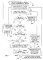
- FIG. 7 is a flow diagram outlining important steps of Monte Carlo simulation code used to model how electrons in an electron beam interact with a resist.
- Preferred implementations of the invention disclosed herein mitigate electron scattering effects that would otherwise make it difficult to achieve high resolution, well-defined features in resist material using electron beam lithography.
- the scattering of electrons by atoms can be modeled by considering that both elastic and inelastic scattering of electrons can occur, and that both kinds of scattering affect the mean free path ⁇ of electrons propagating through a material. If the total elastic cross section and the total inelastic cross section are denoted by ⁇ e and ⁇ in , respectively, then
- ⁇ - 1 ⁇ ⁇ i ⁇ N i ⁇ ( ⁇ i e + ⁇ i in ) ⁇ ( 1 ) in which the summation is over the different types of particles encountered by the electrons (with these different particle types having respective cross sections), and N i represents the number density of particles of type “i”.
- Modeling an electron's trajectory through a substance is most easily done by applying Monte Carlo statistical analysis, in view of equation (1) and accounting for energy losses arising from scattering. Essentially, the respective paths of a large number of electrons are generated using random numbers input into statistical models. This is a well known technique that is described in the literature and is accepted as an accurate physical description of the otherwise computational intractable problem of computing the energy deposited from the electron beam into the substrate.
- the specific code used herein has been exhaustively calibrated against experiment and has proven to be extremely accurate in determining the energy deposited by an energetic electron beam in a resist material overlying a variety of different substrate materials. Further details regarding one such Monte Carlo statistical approach that was used are given below.
- FIG. 2A shows a resist 50 overlying a metal or conductive layer 54 , which in turn overlies a substrate 58 that is preferably insulating.
- FIG. 2A shows a resist 50 overlying a metal or conductive layer 54 , which in turn overlies a substrate 58 that is preferably insulating.
- FIG. 2B shows the case in which a resist 60 overlies a metal or conductive layer 64 , which overlies a material 66 that is preferably insulating (e.g., oxide) and that is in contact with a non-insulating substrate 68 .
- FIG. 2C shows the case in which a resist 70 is in contact with a first non-insulating substrate material 78 a (e.g., silicon), which in turn overlies a material 76 that is preferably insulating and that is in contact with a second non-insulating substrate material 78 b.
- a first non-insulating substrate material 78 a e.g., silicon
- Electric fields may be applied through voltage sources 80 a , 80 b , and 80 c using simple connections, as shown in FIGS. 2A , 2 B, and 2 C, respectively. Even a small battery would suffice, since at most little current will flow; alternatively, the requisite electric potential could be supplied from a power supply.
- a voltage source is applied to a portion of the underlying structure on which the resist resides.
- an electric field is generated across the insulating substrate 58 by connecting leads to the conductive layer 54 and the underside of the substrate 58 , which would be made conductive for this purpose by, e.g., depositing a thin conductive layer (not shown) on the underside.
- an electric field is generated across the insulator 66 by connecting leads to the conductive layer 64 and the substrate 68 .
- an electric field is generated across the insulator 76 by applying the voltage source 80 c to the two non-insulating substrate materials 78 a and 78 b .
- electric field lines 82 a , 82 b , and 82 c are shown in FIGS. 2A , 2 B, and 2 C, respectively.
- the insulating materials 58 , 66 , and 76 may be replaced with materials that are at least partially non-insulating, provided that the voltage sources 80 a , 80 b , and 80 c can provide sufficient current to maintain the desired electric field strength.
- FIG. 3 One set of simulations is shown in FIG. 3 , for which a 30 kV input electron beam of 10 nm diameter is directed onto a 500 nm thick resist layer that in turn overlies a 1 ⁇ m thick layer of SiO 2 on silicon.
- the simulations here were made with the configuration of FIG. 2B in mind, but with the conductive layer 64 being neglected (which is equivalent to assuming that the conductive layer 64 is at most about 10 nm thick).
- This figure shows a family of line spread functions corresponding to different electric field strengths underneath the resist layer. Note that FIG.
- FIG. 3 is a log-log graph of energy absorbed per unit volume of resist per incident electron (plotted along the y-axis) versus lateral distance (plotted along the x-axis), i.e., the distance measured in a plane perpendicular to the direction of the input electron beam, in which “zero distance” is taken to be the center of the input electron beam.
- Each curve in the figure can be thought of as the effective beam profile to which the resist is exposed as a result of electron scattering in the substrate.
- the uppermost curve in FIG. 3 is the effective beam profile for the prior art situation, in which no electric field is introduced. For this curve, significant exposure to the resist is observed at many microns from the center of the input electron beam. For dense feature patterns, extensive correction of proximity effects would be required, since the 10 nm diameter electron beam will be sensed by the resist material out to a lateral distance (as measured away from the center of the input electron beam) of several microns.
- the other curves in FIG. 3 illustrate the effect of applying an electric field across the 1 ⁇ m SiO 2 layer. Even at 0.05 V/nm, it is clear that the dose to the resist is significantly reduced at lateral distances greater than 0.1 ⁇ m. Note that a relatively small potential, 50 V, is required to achieve this electric field across the 1 ⁇ m SiO 2 layer. The proximity exposure decreases further as the strength of the applied electric field is increased. However, an electric field of even modest strength provides substantial benefit and is expected to lead to a significant reduction in the amount of blur in the features written by the e-beam in the resist. Accordingly, by using an electric field in this way, the density of features that can be written into a resist can be substantially increased.
- An electron beam 90 (not shown in FIGS. 2A , 2 C, and 4 , 5 and 6 below) is directed onto the resist 60 , passes through the conductive layer 64 and the insulator 66 , and continues on into the substrate 68 .
- the electrons in the e-beam 90 may undergo scattering events similar to those illustrated in FIG. 1 .
- One or more scattering events 92 in the substrate 68 redirect electrons back into the insulator 66 where they encounter the applied electric field represented by the field lines 82 b . At this point, however, the electrons are deflected by the applied electric field.
- They may be deflected back into the substrate 68 ; they may give up their energy in the insulator 66 , as shown in FIG. 2B ; or they may reenter the conductive layer 64 or even the resist 60 , where they may damage the resist.
- the effect of the applied electric field is to mitigate the latter possibility, thereby improving the fidelity of the pattern written into the resist 60 by reducing proximity effects that otherwise lead to the blurring of features.
- the underlying structure is preferably insulating.
- the underlying structure is preferably insulating.
- this is not as restrictive as one might think.
- masks patterned by e-beam lithography are usually made of quartz or glass, which is electrically insulating.
- prototyping and test structures are often defined on structures that contain an insulating layer directly beneath or very close to the surface of the substrate material, as illustrated in FIGS. 2B and 2C , for example.
- a sacrificial insulating layer can be applied and removed after patterning, or it can be left as part of the substrate.
- the resist 70 would be coated onto the (cleaned) substrate material 78 a .
- the resist coated substrate material 78 a would then be subject to a pre-exposure bake and loaded into the electron beam lithography system (not shown).
- the potential would be applied to the substrate material 78 a , so that an electric field is generated across the insulating layer 76 .
- the electron beam would be swept across the resist coated sample as required to generate the energy deposition profile predetermined by the design and control software of the lithography system. Following exposure, the sample would be removed from the lithography system and then heated or otherwise treated as appropriate for the given resist 70 .
- the resist 70 would then be developed in the appropriate developer, resulting in either the removal of the exposed areas if a “positive” resist is used or the unexposed areas if a “negative” resist is used.
- the resulting pattern in the resist can then be used for a variety of pattern replication techniques, e.g., it can serve as an etch mask or be used for the lift-off of a deposited film.
- the electric field is preferably applied in the region just beneath the surface of the resist-coated workpiece, which is then penetrated by the incident energetic electrons in the electron beam.
- the maximum depth penetrated (Grin range) is dependent on the energy Ep of the incident electron beam and is proportional to Ep 1.75 . For 30 kV electrons, this range is about 15 ⁇ m in silicon; for 100 kV electrons, the Grün range is ⁇ 100 ⁇ m.
- the field is preferably applied as close to the surface of the workpiece as possible and over as large a depth into the workpiece as possible.
- applying a field of 0.1 V/nm over 1000 nm of a SiO 2 positioned directly underneath 500 nm of resist will reduce backscattered electrons by at least 90% at a lateral distance of 1000 nm away from a line source of 30 kV electrons.
- the electric field strength may advantageously be in the range of between 0.002 V/nm and 0.5 V/nm, and is more preferably in the range of between 0.0002 V/nm and 0.1 V/nm.
- the electric field strength may advantageously be in the range of between 0.01 and 0.5 V/nm, and is more preferably in the range of between 0.01 and 0.1 V/nm. While in the above example the percentage of backscattered electrons is reduced by at least 90%, the electric field strength may be selected so that this percentage is at least 50%, or even at least 30%.
- the characteristic dimension of features or lines that may be produced using the methods herein may be at least as small as 10–30 nm, for example.
- This characteristic dimension may be, for example, in the range of between 10 nm and 100 microns, is more preferably in the range of between 30 nm and 5 microns, is still more preferably in the range of between 30 nm and 1000 nm, and is most preferably in the range of between 30 nm and 100 nm.
- Electron beam lithography is generally used in semiconductor manufacturing for mask making and in direct write applications. In both cases, the workpieces may be readily adapted to include a region of electric field beneath the surface of the workpiece.
- the workpiece is generally electrically insulating, so that an electric field could be applied across the entire mask blank.
- a potential of tens of kV might be required.
- the magnitude of the potential can be reduced by orders of magnitude if the workpiece is modified so that the field is only applied over the top few microns of the mask blank.
- FIG. 4 shows a structure for forming such a mask.
- the structure includes an insulating layer such as a silicon dioxide layer 100 , which may range in thickness from 100 nm to 10 ⁇ m, with 1 ⁇ m being a preferred value.
- the silicon dioxide layer 100 is coated with a mask material 104 , e.g., a thin metallic layer such as 15 nm thick Cr.
- a conductive layer 108 On the backside of the layer 100 is a conductive layer 108 , which is advantageously transparent to the wavelength of light for which the mask will be used, e.g., 50–60 nm of ITO (indium tin oxide) is a good choice for work with ultraviolet light.
- ITO indium tin oxide
- a resist material 112 (e.g., 500 nm thick) overlies the mask material 104 , and the conductive layer 108 overlies a mask blank or substrate 116 , such as 6 mm thick fused silica.
- a potential 118 would then be applied between the conducting layers 104 and 108 (which are positioned on the top and backside of the silicon dioxide layer 100 , respectively) to produce, for example, an electric field of 0.1 V/nm (100 V/ ⁇ m).
- the patterning of the mask material 104 is then performed in the standard way by displacing the electron beam over the surface of the workpiece to define the desired pattern in the resist material 112 .
- the resist 112 is then developed and the pattern transferred by an etch process into the thin Cr layer 104 .
- the various layers of FIG. 4 may be deposited using standard chemical vapor deposition (CVD) or plasma enhanced chemical vapor deposition (PECVD) techniques. Note that the potential would be applied between the top Cr layer 104 and the buried conductive (ITO) layer 108 by making an appropriate contact to the buried conductive layer. This could be facilitated by simply masking the silicon dioxide layer 100 layer during the fabrication process to leave the conductive layer 108 exposed around the edge of the mask blank 116 .
- CVD chemical vapor deposition
- PECVD plasma enhanced chemical vapor deposition
- a substrate containing a buried insulating layer is commonly used in the microelectronics industry, e.g., the class of materials known as silicon on insulator (SOI), which is commonly used as a substrate in semiconductor manufacturing.
- FIG. 2C shows such an arrangement, in which the substrate material 78 a (e.g., silicon) overlies the insulator 76 , which in turn overlies the substrate material 78 b (which may include silicon).
- SOI a contact is made to the back of the wafer (corresponding in this example to the underside of the substrate material 78 b ) using any standard technique for making an electrical contact to silicon.
- the substrate material 78 b may be principally silicon but nevertheless conducting as a result of, for example, the implantation or diffusion of electrical dopants and/or the deposition of a thin conductive film such as nickel, molybdenum, aluminum, copper or tungsten on the backside of the substrate 78 b .
- Contact may need to be made to the top silicon layer (corresponding in this example to the substrate material 78 a ) around the edge of the wafer.
- a potential is then applied to generate an electric field greater than 0.01 V/nm for 30 kV incident electrons, with 0.1 V/nm being a more typically preferred value.
- FIG. 5 shows a single layer of resist material 130 .
- a conductive film 134 is applied over the resist material 130 .
- the film 134 may be used for charge deposition and can be a thin layer ( ⁇ 10 nm) of conductive polymer or metal, such as aluminum.
- An electric field is created by applying a potential 138 between the top resist layer 130 and a substrate 142 underlying the resist material 130 . Electron beam lithography would then be performed in the standard manner followed by resist development and pattern transfer.
- a relatively thin imaging resist layer 150 is separated from a thicker resist layer 154 by a thin (e.g., ⁇ 10 nm) conductive layer 158 made of polymer or metal, for example.
- the thicker resist layer 154 is advantageously insensitive to irradiation from an energetic electron beam, and could be applied directly to an underlying conductive workpiece by, for example, spin coating.
- a CVD process could be used to deposit a suitable insulating film 162 of silicon oxide or nitride onto a conductive substrate 166 .
- the thin conductive layer (polymer or metal) 158 would then be applied before the application of the thin imaging resist layer 150 .
- a thin imaging resist layer could be applied before applying a conductive film.
- a potential 170 could be applied between the thin conductive layer 158 and the conductive substrate 166 .
- the patterning of the workpiece would then be performed in the standard way by displacing the electron beam over the surface of the workpiece to define the desired pattern in the top imaging resist layer 150 .
- the resist would then be developed and the pattern transferred by an etch process into the underlying, thicker resist layer 154 .
- the layers 150 , 154 are patterned, they could then be used to transfer the pattern into the workpiece.
- the thicker layer 154 is preferably thin enough (e.g., a thickness of ⁇ 100 nm or less) to permit the end product to have reasonably good feature resolution.
- FIG. 7 shows a flow chart of a Monte Carlo model that was used to generate the results of FIG. 3 and the other results presented herein.
- the model generates a primary electron ( 200 ) that is part of an electron beam incident on a multi-layered structure, which typically would include at least a resist layer and a substrate. This electron is considered to impact the top surface of the structure at a single point in space.
- a random number is then generated ( 205 ) for the purpose of calculating the distance traveled by the electron until it undergoes a collision with material in the structure. This distance is calculated from the random number and the mean free path of the electron in the material of the top layer of the structure.
- modeling steps 215 and 220 represent an enhancement over the prior art.
- the energy lost by the electron is calculated by the continuous slow down approximation (see, for example, H. A. Bethe, supra), with this deposited energy being recorded as a function of position in the structure.
- the position of the electron is checked to see if it has crossed into the next layer of the structure ( 225 ). If the electron has crossed a boundary between two layers, the material properties are updated for that new layer ( 230 ), and the distance traveled by the electron is determined accordingly. Otherwise, the electron's trajectory is tracked along the trajectory segment that has been calculated ( 235 ). If the electron energy is less than an “electron stop energy” chosen to be about a few hundred eV ( 245 ), then the trajectory calculation is terminated ( 255 ), and a new primary electron is generated. This value of a few hundred eV is selected to accelerate the computation and has not been found to result in unacceptably large errors; as a theoretical matter, electron propagation is possible even for arbitrarily small electron energy.
- the nature of the next collision event is calculated by a random number ( 260 ), and expressions are called up or calculated for the elastic and inelastic cross section of an electron in the material in which the electron is located. If the collision is elastic ( 270 ), the new direction of the electron is calculated based on a further random number and expression for the elastic cross section ( 275 ). If the collision is inelastic ( 280 ), a discrete energy loss and a new electron direction are calculated by random numbers and expressions related to the inelastic cross section.
- This discrete energy loss is considered to generate a secondary electron that is tracked independently of the primary electrons ( 285 ), and the entire calculation procedure (steps 205 – 275 ) is repeated, except that secondary electrons do not create tertiary electrons through inelastic collisions (as called out in step 270 ).
- the inelastic energy loss is considered to be deposited into the material at the position of the inelastic collision.
- the energy of the electrons is reduced at each step by the amount deposited into the structure.
- the electrons are tracked until they reach some minimum energy (“electron stop energy”), which is typically on the order of 500 eV. At that point they are considered to move no further, and all their energy is considered to be deposited into the material at that position. Electrons can also leave the structure in which case they are no longer tracked. Electrons that leave back through the top of the substrate are called backscattered electrons. If the structure is thin, electrons can pass through the entire structure and are called transmitted electrons. After an electron has stopped, been backscattered or transmitted, a new primary electron is generated, and the Monte Carlo process of tracking the passage of an electron through the structure is repeated.
- the results of the code are used to generate profiles of energy deposited in the structure.
- the resist layer is usually the most important one, since this is the layer whose deposited energy profile determines the pattern exposed into the resist.
- FIG. 3 is one such example of energy deposition profiles.
- the model described herein has been validated in various ways, including comparing modeling results with experimental results and results from independently written Monte Carlo type simulation routines. The model's limitations become significant only at sub-10 nm dimensions with very well focused beams. At dimensions relevant for the work disclosed herein (>30 nm), the model's predictions are consistent with experimental results to within experimental error (typically a few %).
- media encoded with executable program code to effect any of the modeling methods described herein.
- This code contains executable instructions that may reside, for example, in the random access memory (RAM) of a processor, or on a hard drive or optical drive of a processor.
- the instructions may be stored on a magnetic or optical disk or diskette, a disk drive, magnetic tape, electronic read-only memory, or other appropriate data storage device.
- this program code may be read by a digital processing apparatus such as a processor or computer for performing any one or more of the modeling methods disclosed herein.
Landscapes
- Engineering & Computer Science (AREA)
- Chemical & Material Sciences (AREA)
- Nanotechnology (AREA)
- Physics & Mathematics (AREA)
- Crystallography & Structural Chemistry (AREA)
- General Physics & Mathematics (AREA)
- Manufacturing & Machinery (AREA)
- Condensed Matter Physics & Semiconductors (AREA)
- Analytical Chemistry (AREA)
- Plasma & Fusion (AREA)
- Mathematical Physics (AREA)
- Theoretical Computer Science (AREA)
- Electron Beam Exposure (AREA)
Abstract
Description
- in
FIG. 4 the electric potential is applied between a conductive mask material and a conductive layer; - in
FIG. 5 the electric potential is applied between a conductive film and a substrate; and - in
FIG. 6 the electric potential is applied between a thin conductive layer and a conducting substrate; and
in which the summation is over the different types of particles encountered by the electrons (with these different particle types having respective cross sections), and Ni represents the number density of particles of type “i”.
Claims (49)
Priority Applications (2)
| Application Number | Priority Date | Filing Date | Title |
|---|---|---|---|
| US10/855,096 US7038204B2 (en) | 2004-05-26 | 2004-05-26 | Method for reducing proximity effects in electron beam lithography |
| JP2005153656A JP4453978B2 (en) | 2004-05-26 | 2005-05-26 | Proximity effect reduction method for electron beam lithography |
Applications Claiming Priority (1)
| Application Number | Priority Date | Filing Date | Title |
|---|---|---|---|
| US10/855,096 US7038204B2 (en) | 2004-05-26 | 2004-05-26 | Method for reducing proximity effects in electron beam lithography |
Publications (2)
| Publication Number | Publication Date |
|---|---|
| US20050263722A1 US20050263722A1 (en) | 2005-12-01 |
| US7038204B2 true US7038204B2 (en) | 2006-05-02 |
Family
ID=35424170
Family Applications (1)
| Application Number | Title | Priority Date | Filing Date |
|---|---|---|---|
| US10/855,096 Expired - Fee Related US7038204B2 (en) | 2004-05-26 | 2004-05-26 | Method for reducing proximity effects in electron beam lithography |
Country Status (2)
| Country | Link |
|---|---|
| US (1) | US7038204B2 (en) |
| JP (1) | JP4453978B2 (en) |
Cited By (2)
| Publication number | Priority date | Publication date | Assignee | Title |
|---|---|---|---|---|
| US20060008178A1 (en) * | 2004-07-08 | 2006-01-12 | Seeger Adam A | Simulation of scanning beam images by combination of primitive features extracted from a surface model |
| US20080067421A1 (en) * | 2006-08-16 | 2008-03-20 | Kuei-Wen Cheng | Electron Beam Etching Apparatus and Method for the same |
Families Citing this family (6)
| Publication number | Priority date | Publication date | Assignee | Title |
|---|---|---|---|---|
| US20060183025A1 (en) * | 2005-02-14 | 2006-08-17 | Micron Technology, Inc. | Methods of forming mask patterns, methods of correcting feature dimension variation, microlithography methods, recording medium and electron beam exposure system |
| TWI284790B (en) * | 2005-07-19 | 2007-08-01 | Powerchip Semiconductor Corp | Calibration method for different types of exposure apparatus via using single mask and method for auto-feedback of the best focus |
| JP5063071B2 (en) * | 2006-02-14 | 2012-10-31 | 株式会社ニューフレアテクノロジー | Pattern creating method and charged particle beam drawing apparatus |
| US7827519B2 (en) * | 2006-12-29 | 2010-11-02 | Cadence Design Systems, Inc. | Method, system, and computer program product for preparing multiple layers of semiconductor substrates for electronic designs |
| US7962866B2 (en) | 2006-12-29 | 2011-06-14 | Cadence Design Systems, Inc. | Method, system, and computer program product for determining three-dimensional feature characteristics in electronic designs |
| US8832621B1 (en) | 2011-11-28 | 2014-09-09 | Cadence Design Systems, Inc. | Topology design using squish patterns |
Citations (18)
| Publication number | Priority date | Publication date | Assignee | Title |
|---|---|---|---|---|
| JPS55140229A (en) | 1979-04-20 | 1980-11-01 | Hitachi Ltd | Method for formation of fine pattern |
| GB1604004A (en) | 1977-10-11 | 1981-12-02 | Fujitsu Ltd | Method and apparatus for processing semi-conductor wafers |
| US4323638A (en) | 1980-08-18 | 1982-04-06 | Bell Telephone Laboratories, Incorporated | Reducing charging effects in charged-particle-beam lithography |
| US4350866A (en) | 1977-10-11 | 1982-09-21 | Fujitsu Limited | Discharge device and method for use in processing semiconductor devices |
| JPS57207338A (en) | 1981-06-16 | 1982-12-20 | Fujitsu Ltd | Method for treating resist film for electron beam |
| JPS58140120A (en) | 1982-02-16 | 1983-08-19 | Sanyo Electric Co Ltd | Pattern formation |
| JPS61206223A (en) | 1985-03-08 | 1986-09-12 | Fujitsu Ltd | Formation of pattern |
| JPS61208830A (en) | 1985-03-14 | 1986-09-17 | Toshiba Corp | Charged beam exposure method |
| JPS6425416A (en) | 1987-07-21 | 1989-01-27 | Matsushita Electric Industrial Co Ltd | Electron beam exposure method |
| JPH0191422A (en) | 1987-10-02 | 1989-04-11 | Matsushita Electric Ind Co Ltd | Formation of fine pattern |
| JPH01283825A (en) | 1988-05-10 | 1989-11-15 | Seiko Epson Corp | positive photoresist |
| JPH02192714A (en) | 1989-01-20 | 1990-07-30 | Dainippon Printing Co Ltd | Formation of resist pattern |
| US5112724A (en) * | 1989-11-30 | 1992-05-12 | Texas Instruments Incorporated | Lithographic method |
| JPH0829967A (en) | 1994-07-14 | 1996-02-02 | Hitachi Ltd | Pattern forming method and element forming method |
| US6482558B1 (en) | 2000-10-24 | 2002-11-19 | Advanced Micro Devices, Inc. | Conducting electron beam resist thin film layer for patterning of mask plates |
| US20020177083A1 (en) | 2001-05-25 | 2002-11-28 | Elizabeth Dobisz | Anti-charging layer for beam lithography and mask fabrication |
| US6512237B2 (en) | 1998-12-18 | 2003-01-28 | Kabushiki Kaisha Toshiba | Charged beam exposure method and charged beam exposure apparatus |
| US20030146382A1 (en) | 1998-04-20 | 2003-08-07 | Hitachi, Ltd. | Workpiece holder, semiconductor fabricating apparatus, semiconductor inspecting apparatus, circuit pattern inspecting apparatus, charged particle beam application apparatus, calibrating substrate, workpiece holding method, circuit pattern inspecting method, and charged particle beam application method |
Family Cites Families (3)
| Publication number | Priority date | Publication date | Assignee | Title |
|---|---|---|---|---|
| US146382A (en) * | 1874-01-13 | Improvement in burglar-proof safes | ||
| US177083A (en) * | 1876-05-09 | Improvement in combined kettles and cooking apparatus | ||
| US203311A (en) * | 1878-05-07 | Improvement in stalk-cutters |
-
2004
- 2004-05-26 US US10/855,096 patent/US7038204B2/en not_active Expired - Fee Related
-
2005
- 2005-05-26 JP JP2005153656A patent/JP4453978B2/en not_active Expired - Fee Related
Patent Citations (19)
| Publication number | Priority date | Publication date | Assignee | Title |
|---|---|---|---|---|
| GB1604004A (en) | 1977-10-11 | 1981-12-02 | Fujitsu Ltd | Method and apparatus for processing semi-conductor wafers |
| US4350866A (en) | 1977-10-11 | 1982-09-21 | Fujitsu Limited | Discharge device and method for use in processing semiconductor devices |
| JPS55140229A (en) | 1979-04-20 | 1980-11-01 | Hitachi Ltd | Method for formation of fine pattern |
| US4323638A (en) | 1980-08-18 | 1982-04-06 | Bell Telephone Laboratories, Incorporated | Reducing charging effects in charged-particle-beam lithography |
| JPS57207338A (en) | 1981-06-16 | 1982-12-20 | Fujitsu Ltd | Method for treating resist film for electron beam |
| JPS58140120A (en) | 1982-02-16 | 1983-08-19 | Sanyo Electric Co Ltd | Pattern formation |
| JPS61206223A (en) | 1985-03-08 | 1986-09-12 | Fujitsu Ltd | Formation of pattern |
| JPS61208830A (en) | 1985-03-14 | 1986-09-17 | Toshiba Corp | Charged beam exposure method |
| JPS6425416A (en) | 1987-07-21 | 1989-01-27 | Matsushita Electric Industrial Co Ltd | Electron beam exposure method |
| JPH0191422A (en) | 1987-10-02 | 1989-04-11 | Matsushita Electric Ind Co Ltd | Formation of fine pattern |
| JPH01283825A (en) | 1988-05-10 | 1989-11-15 | Seiko Epson Corp | positive photoresist |
| JPH02192714A (en) | 1989-01-20 | 1990-07-30 | Dainippon Printing Co Ltd | Formation of resist pattern |
| US5112724A (en) * | 1989-11-30 | 1992-05-12 | Texas Instruments Incorporated | Lithographic method |
| JPH0829967A (en) | 1994-07-14 | 1996-02-02 | Hitachi Ltd | Pattern forming method and element forming method |
| US20030146382A1 (en) | 1998-04-20 | 2003-08-07 | Hitachi, Ltd. | Workpiece holder, semiconductor fabricating apparatus, semiconductor inspecting apparatus, circuit pattern inspecting apparatus, charged particle beam application apparatus, calibrating substrate, workpiece holding method, circuit pattern inspecting method, and charged particle beam application method |
| US6512237B2 (en) | 1998-12-18 | 2003-01-28 | Kabushiki Kaisha Toshiba | Charged beam exposure method and charged beam exposure apparatus |
| US6482558B1 (en) | 2000-10-24 | 2002-11-19 | Advanced Micro Devices, Inc. | Conducting electron beam resist thin film layer for patterning of mask plates |
| US20020177083A1 (en) | 2001-05-25 | 2002-11-28 | Elizabeth Dobisz | Anti-charging layer for beam lithography and mask fabrication |
| US20030203311A1 (en) | 2001-05-25 | 2003-10-30 | Elizabeth Dobisz | Anti-charging layer for beam lithography and mask fabrication |
Non-Patent Citations (4)
| Title |
|---|
| C. R. K. Marrian et al., "Modelling of electron elastic and inelastic scattering", Journal Vac. Science Technology B., vol. 14, No. 6, Nov./Dec. 1996, pp. 3864-3869. |
| R. J. Hawryluk et al., "Energy dissipation in a thin polymer film by electron beam scattering*", Journal of Applied Physics, vol. 45, No. 6, Jun. 1974, pp. 2551-2566. |
| R. Shimizu et al., "Monte Carlo modelling of electron-solid interactions", Rep. Prog. Phys., 1992, pp. 487-531. |
| Z.-J. Ding et al., "A Monte Carlo Modeling of Electron Interaction with Solids Including Cascade Secondary Electron Production", Scanning, vol. 18, 1996, pp. 92-113. |
Cited By (2)
| Publication number | Priority date | Publication date | Assignee | Title |
|---|---|---|---|---|
| US20060008178A1 (en) * | 2004-07-08 | 2006-01-12 | Seeger Adam A | Simulation of scanning beam images by combination of primitive features extracted from a surface model |
| US20080067421A1 (en) * | 2006-08-16 | 2008-03-20 | Kuei-Wen Cheng | Electron Beam Etching Apparatus and Method for the same |
Also Published As
| Publication number | Publication date |
|---|---|
| US20050263722A1 (en) | 2005-12-01 |
| JP4453978B2 (en) | 2010-04-21 |
| JP2005340831A (en) | 2005-12-08 |
Similar Documents
| Publication | Publication Date | Title |
|---|---|---|
| TWI605302B (en) | Method for critical dimension consistency using charged particle beam lithography | |
| US8057970B2 (en) | Method and system for forming circular patterns on a surface | |
| US9341936B2 (en) | Method and system for forming a pattern on a reticle using charged particle beam lithography | |
| US10431422B2 (en) | Method and system for dimensional uniformity using charged particle beam lithography | |
| WO2010025060A2 (en) | Method for design and manufacture of a reticle using variable shaped beam lithography | |
| JPH0778737A (en) | Charged particle beam exposure method and charged particle beam exposure apparatus | |
| JP2010062562A (en) | Method for manufacturing semiconductor device on substrate, method for fracturing or mask data preparation for charged particle beam lithography, method and system for forming a plurality of circular patterns on surface, and system for fracturing or mask data preparation to be used in charged particle beam lithography | |
| JP4871536B2 (en) | Process for controlling proximity correction | |
| US7038204B2 (en) | Method for reducing proximity effects in electron beam lithography | |
| KR102201802B1 (en) | Method and system for dimensional uniformity using charged particle beam lithography | |
| Murata et al. | Monte Carlo methods and microlithography simulation for electron and X-ray beams | |
| US6972417B2 (en) | Apparatus and methods for patterning a reticle blank by electron-beam inscription with reduced exposure of the reticle blank by backscattered electrons | |
| TWI514437B (en) | Method and system for fracturing a pattern using charged particle beam lithography with multiple exposure passes | |
| CN104520769A (en) | Substrate for high-resolution electronic lithography and corresponding lithography method | |
| KR20020018280A (en) | Method of electron beam lithography by double exposure and fabrication method of photomask using the same | |
| Lu et al. | Proximity and heating effects during electron-beam patterning of ultraviolet lithography masks | |
| Choi et al. | Pattern placement error due to resist charging effect at 50kV e-beam writer: mechanism and its correction | |
| Wasson et al. | Writing, repairing, and inspecting of extreme ultraviolet lithography reticles considering the impact of the materials | |
| JP2781941B2 (en) | Electron beam writing method | |
| US12248248B2 (en) | Electron beam lithography with a bilayer resist | |
| Rhee et al. | Proximity effect reduction in x‐ray mask making using thin silicon dioxide layers | |
| Choi et al. | Degradation of pattern quality due to strong electron scattering in EUV mask | |
| Mladenov et al. | Computer simulation of electron and ion beam lithography of nanostructures | |
| Vutova et al. | Computer simulation of micro-and nano-structures at electron and ion lithography | |
| Chen et al. | Impact of proximity model inaccuracy on patterning in electron beam lithography |
Legal Events
| Date | Code | Title | Description |
|---|---|---|---|
| AS | Assignment |
Owner name: INTERNATIONAL BUSINESS MACHINES CORPORATION, NEW Y Free format text: ASSIGNMENT OF ASSIGNORS INTEREST;ASSIGNORS:MARRIAN, CHRISTIE RODERICK KINGSLEY;RETTNER, CHARLES THOMAS;REEL/FRAME:015432/0321 Effective date: 20040526 |
|
| FEPP | Fee payment procedure |
Free format text: PAYOR NUMBER ASSIGNED (ORIGINAL EVENT CODE: ASPN); ENTITY STATUS OF PATENT OWNER: LARGE ENTITY |
|
| FPAY | Fee payment |
Year of fee payment: 4 |
|
| REMI | Maintenance fee reminder mailed | ||
| LAPS | Lapse for failure to pay maintenance fees | ||
| STCH | Information on status: patent discontinuation |
Free format text: PATENT EXPIRED DUE TO NONPAYMENT OF MAINTENANCE FEES UNDER 37 CFR 1.362 |
|
| STCH | Information on status: patent discontinuation |
Free format text: PATENT EXPIRED DUE TO NONPAYMENT OF MAINTENANCE FEES UNDER 37 CFR 1.362 |
|
| FP | Lapsed due to failure to pay maintenance fee |
Effective date: 20140502 |
|
| AS | Assignment |
Owner name: GLOBALFOUNDRIES U.S. 2 LLC, NEW YORK Free format text: ASSIGNMENT OF ASSIGNORS INTEREST;ASSIGNOR:INTERNATIONAL BUSINESS MACHINES CORPORATION;REEL/FRAME:036550/0001 Effective date: 20150629 |
|
| AS | Assignment |
Owner name: GLOBALFOUNDRIES INC., CAYMAN ISLANDS Free format text: ASSIGNMENT OF ASSIGNORS INTEREST;ASSIGNORS:GLOBALFOUNDRIES U.S. 2 LLC;GLOBALFOUNDRIES U.S. INC.;REEL/FRAME:036779/0001 Effective date: 20150910 |