US7023070B2 - Semiconductor device - Google Patents
Semiconductor device Download PDFInfo
- Publication number
- US7023070B2 US7023070B2 US10/748,255 US74825503A US7023070B2 US 7023070 B2 US7023070 B2 US 7023070B2 US 74825503 A US74825503 A US 74825503A US 7023070 B2 US7023070 B2 US 7023070B2
- Authority
- US
- United States
- Prior art keywords
- terminal
- chip
- fuse
- film
- semiconductor device
- Prior art date
- Legal status (The legal status is an assumption and is not a legal conclusion. Google has not performed a legal analysis and makes no representation as to the accuracy of the status listed.)
- Expired - Lifetime, expires
Links
Images


Classifications
-
- H—ELECTRICITY
- H10—SEMICONDUCTOR DEVICES; ELECTRIC SOLID-STATE DEVICES NOT OTHERWISE PROVIDED FOR
- H10W—GENERIC PACKAGES, INTERCONNECTIONS, CONNECTORS OR OTHER CONSTRUCTIONAL DETAILS OF DEVICES COVERED BY CLASS H10
- H10W42/00—Arrangements for protection of devices
-
- H—ELECTRICITY
- H10—SEMICONDUCTOR DEVICES; ELECTRIC SOLID-STATE DEVICES NOT OTHERWISE PROVIDED FOR
- H10W—GENERIC PACKAGES, INTERCONNECTIONS, CONNECTORS OR OTHER CONSTRUCTIONAL DETAILS OF DEVICES COVERED BY CLASS H10
- H10W42/00—Arrangements for protection of devices
- H10W42/60—Arrangements for protection of devices protecting against electrostatic charges or discharges, e.g. Faraday shields
-
- H—ELECTRICITY
- H10—SEMICONDUCTOR DEVICES; ELECTRIC SOLID-STATE DEVICES NOT OTHERWISE PROVIDED FOR
- H10W—GENERIC PACKAGES, INTERCONNECTIONS, CONNECTORS OR OTHER CONSTRUCTIONAL DETAILS OF DEVICES COVERED BY CLASS H10
- H10W42/00—Arrangements for protection of devices
- H10W42/80—Arrangements for protection of devices protecting against overcurrent or overload, e.g. fuses or shunts
-
- H—ELECTRICITY
- H10—SEMICONDUCTOR DEVICES; ELECTRIC SOLID-STATE DEVICES NOT OTHERWISE PROVIDED FOR
- H10W—GENERIC PACKAGES, INTERCONNECTIONS, CONNECTORS OR OTHER CONSTRUCTIONAL DETAILS OF DEVICES COVERED BY CLASS H10
- H10W72/00—Interconnections or connectors in packages
-
- H—ELECTRICITY
- H10—SEMICONDUCTOR DEVICES; ELECTRIC SOLID-STATE DEVICES NOT OTHERWISE PROVIDED FOR
- H10D—INORGANIC ELECTRIC SEMICONDUCTOR DEVICES
- H10D89/00—Aspects of integrated devices not covered by groups H10D84/00 - H10D88/00
- H10D89/60—Integrated devices comprising arrangements for electrical or thermal protection, e.g. protection circuits against electrostatic discharge [ESD]
- H10D89/601—Integrated devices comprising arrangements for electrical or thermal protection, e.g. protection circuits against electrostatic discharge [ESD] for devices having insulated gate electrodes, e.g. for IGFETs or IGBTs
- H10D89/611—Integrated devices comprising arrangements for electrical or thermal protection, e.g. protection circuits against electrostatic discharge [ESD] for devices having insulated gate electrodes, e.g. for IGFETs or IGBTs using diodes as protective elements
-
- H—ELECTRICITY
- H10—SEMICONDUCTOR DEVICES; ELECTRIC SOLID-STATE DEVICES NOT OTHERWISE PROVIDED FOR
- H10W—GENERIC PACKAGES, INTERCONNECTIONS, CONNECTORS OR OTHER CONSTRUCTIONAL DETAILS OF DEVICES COVERED BY CLASS H10
- H10W20/00—Interconnections in chips, wafers or substrates
- H10W20/40—Interconnections external to wafers or substrates, e.g. back-end-of-line [BEOL] metallisations or vias connecting to gate electrodes
- H10W20/49—Adaptable interconnections, e.g. fuses or antifuses
- H10W20/493—Fuses, i.e. interconnections changeable from conductive to non-conductive
-
- H—ELECTRICITY
- H10—SEMICONDUCTOR DEVICES; ELECTRIC SOLID-STATE DEVICES NOT OTHERWISE PROVIDED FOR
- H10W—GENERIC PACKAGES, INTERCONNECTIONS, CONNECTORS OR OTHER CONSTRUCTIONAL DETAILS OF DEVICES COVERED BY CLASS H10
- H10W72/00—Interconnections or connectors in packages
- H10W72/01—Manufacture or treatment
- H10W72/012—Manufacture or treatment of bump connectors, dummy bumps or thermal bumps
- H10W72/01251—Changing the shapes of bumps
- H10W72/01255—Changing the shapes of bumps by using masks
-
- H—ELECTRICITY
- H10—SEMICONDUCTOR DEVICES; ELECTRIC SOLID-STATE DEVICES NOT OTHERWISE PROVIDED FOR
- H10W—GENERIC PACKAGES, INTERCONNECTIONS, CONNECTORS OR OTHER CONSTRUCTIONAL DETAILS OF DEVICES COVERED BY CLASS H10
- H10W72/00—Interconnections or connectors in packages
- H10W72/071—Connecting or disconnecting
- H10W72/072—Connecting or disconnecting of bump connectors
- H10W72/07251—Connecting or disconnecting of bump connectors characterised by changes in properties of the bump connectors during connecting
- H10W72/07252—Connecting or disconnecting of bump connectors characterised by changes in properties of the bump connectors during connecting changes in structures or sizes
-
- H—ELECTRICITY
- H10—SEMICONDUCTOR DEVICES; ELECTRIC SOLID-STATE DEVICES NOT OTHERWISE PROVIDED FOR
- H10W—GENERIC PACKAGES, INTERCONNECTIONS, CONNECTORS OR OTHER CONSTRUCTIONAL DETAILS OF DEVICES COVERED BY CLASS H10
- H10W72/00—Interconnections or connectors in packages
- H10W72/20—Bump connectors, e.g. solder bumps or copper pillars; Dummy bumps; Thermal bumps
- H10W72/221—Structures or relative sizes
- H10W72/227—Multiple bumps having different sizes
-
- H—ELECTRICITY
- H10—SEMICONDUCTOR DEVICES; ELECTRIC SOLID-STATE DEVICES NOT OTHERWISE PROVIDED FOR
- H10W—GENERIC PACKAGES, INTERCONNECTIONS, CONNECTORS OR OTHER CONSTRUCTIONAL DETAILS OF DEVICES COVERED BY CLASS H10
- H10W72/00—Interconnections or connectors in packages
- H10W72/20—Bump connectors, e.g. solder bumps or copper pillars; Dummy bumps; Thermal bumps
- H10W72/251—Materials
- H10W72/252—Materials comprising solid metals or solid metalloids, e.g. PbSn, Ag or Cu
-
- H—ELECTRICITY
- H10—SEMICONDUCTOR DEVICES; ELECTRIC SOLID-STATE DEVICES NOT OTHERWISE PROVIDED FOR
- H10W—GENERIC PACKAGES, INTERCONNECTIONS, CONNECTORS OR OTHER CONSTRUCTIONAL DETAILS OF DEVICES COVERED BY CLASS H10
- H10W72/00—Interconnections or connectors in packages
- H10W72/90—Bond pads, in general
- H10W72/921—Structures or relative sizes of bond pads
- H10W72/923—Bond pads having multiple stacked layers
-
- H—ELECTRICITY
- H10—SEMICONDUCTOR DEVICES; ELECTRIC SOLID-STATE DEVICES NOT OTHERWISE PROVIDED FOR
- H10W—GENERIC PACKAGES, INTERCONNECTIONS, CONNECTORS OR OTHER CONSTRUCTIONAL DETAILS OF DEVICES COVERED BY CLASS H10
- H10W72/00—Interconnections or connectors in packages
- H10W72/90—Bond pads, in general
- H10W72/941—Dispositions of bond pads
- H10W72/9415—Dispositions of bond pads relative to the surface, e.g. recessed, protruding
-
- H—ELECTRICITY
- H10—SEMICONDUCTOR DEVICES; ELECTRIC SOLID-STATE DEVICES NOT OTHERWISE PROVIDED FOR
- H10W—GENERIC PACKAGES, INTERCONNECTIONS, CONNECTORS OR OTHER CONSTRUCTIONAL DETAILS OF DEVICES COVERED BY CLASS H10
- H10W72/00—Interconnections or connectors in packages
- H10W72/90—Bond pads, in general
- H10W72/941—Dispositions of bond pads
- H10W72/944—Dispositions of multiple bond pads
- H10W72/9445—Top-view layouts, e.g. mirror arrays
-
- H—ELECTRICITY
- H10—SEMICONDUCTOR DEVICES; ELECTRIC SOLID-STATE DEVICES NOT OTHERWISE PROVIDED FOR
- H10W—GENERIC PACKAGES, INTERCONNECTIONS, CONNECTORS OR OTHER CONSTRUCTIONAL DETAILS OF DEVICES COVERED BY CLASS H10
- H10W72/00—Interconnections or connectors in packages
- H10W72/90—Bond pads, in general
- H10W72/951—Materials of bond pads
- H10W72/952—Materials of bond pads comprising metals or metalloids, e.g. PbSn, Ag or Cu
Definitions
- the present invention relates to a semiconductor device, and more particularly to an external connection terminal for preventing electrostatic discharge damage.
- COG Chip On Glass
- a COG package gold bumps or solder bumps for packaging on a substrate are formed directly on the semiconductor device chip (hereafter called a “device chip”), and the bumps on the device chip are bonded with a metal wiring printed on the glass or ceramic substrate to be connected with external equipment.
- the packaging area for the substrate is the same size as the device chip, extremely high density packaging is possible.
- the voltage supplied from an external power supply cannot be used for operation of the semiconductor integrated circuit as is, but is used for internal operation after performing voltage adjustment.
- Voltage adjustment is performed by amplifying the reference voltage generated in the semiconductor integrated circuit by an operational amplifier (hereinafter called OP-amp) using the forward voltage of the diode. This voltage adjustment is performed to prevent abnormal functioning of the semiconductor integrated circuit which occurs when the supply voltage from the external power supply is unstable.
- Transistors constituting the OP-amp may have some dispersion of threshold voltage depending on the wafer or the chip. If threshold voltage changes, the amplification characteristics of the OP-amp also changes. When the output voltage of the OP-amp deviates from a desired value, the resistance value of the feedback resistance of the OP-amp is adjusted by blowing out a specific fuse, so that the output voltage becomes a predetermined value.
- FIG. 9 (A) shows an example of a general amplification circuit using an OP-amp.
- the internally generated reference voltage (hereafter called “reference voltage”) V 0 generated in the semiconductor integrated circuit is amplified by the OP-amp 200 , and is output as the reference voltage for device driving (hereafter also called “output voltage”) V 0 ′, which is used for driving the semiconductor integrated circuit, for example.
- the output voltage V 0 ′ of the OP-amp 200 is determined by the resistance value Ri of the resistance element 202 and the resistance value Rf on the feedback resistance 204 .
- the resistance element 202 is comprised of a fixed resistance element of which the resistance value does not change, and the feedback resistance 204 is comprised of a variable resistance element. If the output voltage V 0 ′ of the OP-amp deviates from a desired value, the output voltage V 0 ′ is adjusted by changing the resistance value Rf of the feedback resistance 204 .
- FIG. 9 (B) shows a circuit for resistance value adjustment of the feedback resistance 204 .
- the circuit for resistance value adjustment where PMOS is integrated, is connected to each of the plurality of resistance elements in parallel.
- This circuit for resistance value adjustment is connected with a reference voltage (VDD) via the inverter and the pull-up resistance elements 210 a – 210 c , and is also connected to the ground (GND) potential via the fuses 206 a – 206 c .
- the fuses 206 a – 206 c have protective resistance elements 208 a – 208 c respectively, for protecting the circuit for resistance value adjustment when fuses are blown out.
- FIG. 10 shows a schematic of a general COG package.
- the device chip 230 comprises fuse terminals and chip terminals which have a protective circuit.
- bumps 232 of the chip terminals are arranged in a line along the edge, and a plurality of bumps 234 of the fuse terminals, which are lined up in a line, are disposed in the inner area of the bumps 232 of the chip terminals.
- FIG. 11 shows an example of the protective circuit used for the chip terminal.
- the protective circuit is disposed between the chip terminal 212 and the internal circuit 213 .
- a protective diode 214 connected to the reference voltage (VDD) and a protective diode 216 connected to the ground potential (GND) are disposed.
- the resistance element 218 is connected to the internal circuit 213 via the inverter 220 .
- This protective circuit protects the internal circuit 213 from electrostatic discharge damage by discharging an electrostatic surge which enters the chip terminal to VDD via the protective diode 214 or to GND via the protective diode 216 .
- a fuse terminal for connecting with external equipment is disposed also in a circuit which has a fuse.
- the fuse terminal is not led out as an external terminal to be connected with the external power supply, but is sealed in the resin. Therefore the fuse terminal does not have the protective circuit which the chip terminal has, since the fuse terminal is not exposed to static electricity.
- the heights of the bumps of the device chip and the external substrate to be connected are formed to be high in one and low in the other. Also the heights of the adjacent bumps on the device chip and the external substrate are formed to be different, so the heights of the bonding faces of the adjacent bumps are different, and contact between the bump electrodes is prevented.
- the fuse terminal In a conventional resin sealing type package, the fuse terminal is not led outside, so it is not exposed to electrostatic discharge damage during packaging, and does not require the protective circuit.
- the COG package bumps for connection are formed for the fuse terminal as well as the other chip terminals, so the fuse terminal is led out as a terminal to be connected to the outside. Therefore in the device chip having a fuse, electrostatic discharge damage by a charged external substrate tends to occur when it is connected with the external substrate.
- FIG. 12 shows a schematic of the electrostatic discharge phenomena in the packaging step of the COG package.
- the device chip 244 is already connected to the external substrate 240 .
- the device chip 230 comprising a circuit, which has the fuse shown in FIG. 10 .
- the external substrate 240 is made of glass or ceramic, so it is very easily charged.
- electrostatic discharge occurs in the fuse terminal 234 or the chip terminal 232 . If discharge occurs to the chip terminal 232 , electrostatic discharge damage does not occur since the chip terminal 232 has a protective circuit. If the electrostatic discharge 246 occurs to the fuse terminal 234 , however, electrostatic discharge damage occurs. In other words, the fuse in the circuit of the semiconductor integrated circuit is blown out, and the resistance value, which has been adjusted to a desired resistance value, changes.
- a protective circuit similar to that of the chip circuit is included in the fuse terminal, the occupied area of the chip increases. This increases the chip size, which also increases chip cost. Also a general resin sealing type chip does not have a protective circuit in the fuse terminal, so it cannot be used for a COG type chip as is. Therefore it is necessary to develop a new device chip where a protective circuit is disposed in a fuse terminal.
- the semiconductor device comprises fuse terminals provided on a chip substrate surface and a discharge contribution terminal which is provided at the upper side on the chip substrate surface, and of which the height from the chip substrate surface to the top face is higher than the height of the top face of the fuse terminals.
- the chip substrate surface refers to the surface of the substrate where a device chip is provided, and includes the surface of the isolation film if the latter surface appears at the former surface.
- the top face refers to the surface of the formed bumps.
- the height from the chip substrate surface to the top face of the electrode terminal refers to the height up to the highest position of the top face of the electrode terminal if the top face is not flat.
- the fuse terminal is an electrode terminal to be connected to a circuit which has a fuse (e.g. fuse for changing the resistance value of the variable resistance element).
- the top face of the discharge contribution terminal is formed to be higher than the top face of the fuse terminal, so when the device chip is mounted on a charged external substrate, the discharge contribution terminal contacts the terminal of the external substrate before the fuse terminal, and static electricity is discharged.
- the fuse terminal contacts the terminal of the external substrate, static electricity has already been discharged, so the discharge of static electricity does not occur to the fuse terminal. Therefore electrostatic discharge damage of a semiconductor integrated circuit which has a fuse can be prevented.
- the height from the substrate surface to the top face of the discharge contribution terminal is formed to be higher than the height from the substrate surface to the top face of the fuse terminal, so the fuse terminal does not need a new protective circuit, and the area occupied in the chip does not increase.
- the fuse terminal is formed by directly layering a plurality of conductive layers sequentially and forming a bump on the top conductive layer.
- the discharged contribution terminal is formed by layering a plurality of conductive layers sequentially with inter-layer insulation film intervened, and forming a bump on the top conductive layer.
- the number of layers of the conductive layers in the fuse terminal and the number of layers of the conductive layers in the discharge contribution terminal are the same, and the conductive layers in the sample place in the fuse terminal and the discharge contribution terminal are formed in the same way with the same material.
- the conductive layers of the fuse terminal and the discharge contribution terminal are formed with the same material in the same way, except that the conductive layers of the fuse terminal are directly layered, so the height from the chip substrate surface to the top face of the discharge contribution terminal can be easily formed to be higher than the height from the chip substrate surface to the top face of the fuse terminal. Also since the general manufacturing steps are integrated with the manufacturing method of the semiconductor device, it is unnecessary to add a special step, and the present manufacturing method can be applied to a wide range of semiconductor integrated circuits.
- FIG. 1 is a diagram depicting the semiconductor device of the first embodiment according to the present invention.
- FIGS. 2 (A) and 2 (B) are diagrams depicting the structure of the semiconductor device of the first embodiment according to the present invention.
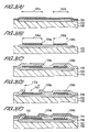
- FIGS. 3 (A)– 3 (E) are cross-sectional views depicting the manufacturing steps of the first embodiment according to the present invention.
- FIGS. 4 (A)– 4 (D) are cross-sectional views depicting the manufacturing steps of the first embodiment according to the present invention.
- FIGS. 5 (A)– 5 (D) are cross-sectional views depicting the manufacturing steps of the first embodiment according to the present invention.
- FIG. 6 is a diagram depicting the semiconductor device of the second embodiment according to the present invention.
- FIGS. 7 (A) and 7 (B) are diagrams depicting the structure of the semiconductor device of the second embodiment according to the present invention.
- FIG. 8 is a diagram depicting a variant form of the semiconductor device of the second embodiment of the present invention.
- FIGS. 9 (A) and 9 (B) are diagrams depicting an example of an amplification circuit which has a fuse
- FIG. 10 is a diagram depicting a general COG package
- FIG. 11 is a circuit diagram depicting a general protective circuit
- FIG. 12 is a schematic depicting the electrostatic discharge phenomena in the COG packaging step.
- a silicon substrate is used for the chip substrate
- the discharge contribution terminal is formed as the chip terminal
- FIG. 1 is a plan view of the device chip 10 of the first embodiment, which is viewed from the top.
- bumps 132 a of the fuse terminals and bumps 132 b of the chip terminals are disposed on the top surface of the device chip 10 .
- the bumps 132 a of the fuse terminals are arranged in a line at the inner side of the device chip surface, and the bumps 132 b of the chip terminals are arranged in a line at the outer side of the surface, along the edge of the device chip surface.
- the bump 132 a of the fuse terminal is indicated by a double line square
- the bump 132 b of the chip terminal is indicated by a single line square.
- FIG. 2 (A) shows the layout of each layer film formation area and the opening area in the area A in FIG. 1 when the semiconductor device of the first embodiment is viewed from the upper side of the device. Only the range where one fuse terminal and one chip terminal are adjacent to each other is extracted and shown in the drawing of FIGS. 2 (A) and 2 (B).
- the polysilicon formation area 106 a is set, and the first metal formation area 116 a is set inside the polysilicon formation area 106 a .
- the second opening area 122 a is set inside the first metal formation area 116 a
- the first opening area 112 a is set inside the second opening area 122 a .
- the second metal formation area 126 a is set inside the first opening area 112 a
- the protective film opening area 130 a is set inside the second metal formation area 126 a.
- the first metal film is etched at the same time when the second metal film is etched, and is formed to be the same shape in the later mentioned manufacturing steps of this semiconductor device.
- the polysilicon film 104 a plays the role of an etching stopper.
- the entire bottom face of the second metal film 124 a is connected to the first metal film 114 a ′ without forming an area where the second interlayer insulating film or interlayer dielectric 118 remains in the lower layer of the second metal film 124 a
- the entire bottom face of the first metal film 114 a ′ is connected to the polysilicon film 104 a without forming an area where the first inter-layer insulation film 108 remains in the lower layer of the first metal film 114 a′.
- the polysilicon formation area 106 b , the first metal formation area 116 b and the second metal formation area 126 b are set as the same area, and inside thereof, the protective film opening area 130 b is set.
- the polysilicon formation area 106 b , the first metal formation area 116 b and the second metal formation area 126 b are simply layered so as to be insulated via the first interlayer insulating film or interlayer dielectric 108 or the second interlayer insulating film 118 , therefore these formation areas are the same size, but need not be.
- FIG. 2 (B) is a cross-sectional view of FIG. 2 (A) taken along the broken line X–X′.
- the field oxide film 102 is formed as the isolation area.
- the fuse terminal 103 a and the chip terminal 103 b are formed respectively.
- the polysilicon film 104 b , the first interlayer insulating film 108 , the first metal film 114 b , the second interlayer insulating film 118 , the second metal film 124 b and the protective film 128 are sequentially layered on the field oxide film 102 .
- the protective film 128 the protective film opening section 129 b is formed therethrough at the protective film opening area 130 b inside the second metal formation area 126 b .
- the bump 132 b is formed in the area which includes the protective film opening area 130 b on the second metal film 124 b .
- the chip terminal 103 b is comprised of the second metal film 124 b and the bump 132 b.
- the polysilicon film 104 a , the first interlayer insulating film 108 , the first metal film 114 a ′, the second interlayer insulating film 118 , the second metal film 124 a and the protective film 128 are sequentially layered on the field oxide film 102 , just like the chip terminal formation area 101 b .
- the first opening area 112 a is opened, and the polysilicon film 104 a and the first metal film 114 a ′ are directly connected.
- the second opening area 122 a is opened, and the first metal film 114 a ′ and the second metal film 124 a are directly connected.
- the protective film 128 the protective film opening 129 a is formed therethrough at the protective film opening area 130 a inside the second metal formation area 126 a .
- the bump 132 a is formed in the area which includes the protective film opening area 130 a on the second metal film 124 a .
- the fuse terminal 103 a is comprised of the polysilicon film 104 a , the first metal film 114 a ′, the second metal film 124 a and the bump 132 a.
- the mid-portions of the bumps 132 a and 132 b are omitted in FIG. 2 (B), since the film thickness thereof is much thicker than that of other films.
- the above mentioned polysilicon films 104 a and 104 b , the first metal films 114 a ′ and 114 b , and the second metal films 124 a and 124 b are all conductive films (also called conductive layers), and are formed by being isolated from a part of the respective interconnecting layer or from the interconnecting layer when the interconnecting layer is formed.
- the polysilicon film 104 a , the first metal film 114 a ′, the second metal film 124 a and the bump 132 a constitute the fuse terminal
- the second metal film 124 b and the bump 132 b constitute the discharge contribution terminal which also functions as the chip terminal.
- the above mentioned configuration of the fuse terminal and the discharge contribution terminal is set in this way for explanation, and the conductive layers to be set as the fuse terminal and the discharge contribution terminal are not limited to the above description.
- the fuse terminal 103 a and the chip terminal 103 b are electrically connected to the power supply wiring of the device chip by one of the above mentioned conductive layers.
- layered films which have a same name are formed simultaneously in the fuse terminal formation area 101 a and the chip terminal formation area 101 b , so they are formed to be the same film thickness.
- the film thickness of the respective layered films are, polysilicon film: h 1 , first inter-layer insulation film: h 2 , first metal film: h 3 , second inter-layer insulation film: h 4 , second metal film: h 5 , protective film: h 6 and bump: h 7 .
- the chip substrate surface 136 becomes the reference to compare the height of the top face of each terminal.
- the surface of the field oxide film 102 where each terminal is formed is used as the chip substrate surface 136 to be the reference.
- the respective film thickness is indicated by the arrow marks.
- the height Hf of the fuse terminal 103 a is the sum of h 1 , h 3 , h 5 , h 6 and h 7
- the height Hc of the chip terminal 103 b is the sum of h 1 , h 2 , h 3 , h 4 , h 5 , h 6 and h 7 .
- the height Hf of the fuse terminal does not include the film thickness h 2 of the first interlayer insulating film and the film thickness h 4 of the second interlayer insulating film
- the height Hc of the chip terminal is higher for the amount of the sum of the film thickness h 2 of the first interlayer insulating film and the film thickness h 4 of the second interlayer insulating film.
- the COG type device chip 10 is approached to the external substrate (e.g. glass or ceramic substrate), which is easily charged, to be connected to external equipment, the chip terminal, which is formed to be higher than the fuse terminal, contacts the external substrate first.
- the static electricity charged on the external substrate is discharged via the protective circuit of the chip terminal. Therefore the discharge of static electricity does not occur to the fuse terminal, and electrostatic discharge damage of the fuse circuit can be prevented.
- Field oxide film 102 is formed on the silicon substrate 100 .
- This field oxide film 102 is formed by a known thermal oxidation method.
- the polysilicon film 104 for the interconnecting is formed ( FIG. 3 (A)).
- This polysilicon film 104 is patterned by a known photolithography etching technology.
- the polysilicon film 104 a is formed at the polysilicon formation area 106 a inside the fuse terminal formation area 101 a
- the polysilicon film 104 b is formed at the polysilicon formation area 106 b inside the chip terminal formation area 101 b ( FIG. 3 (B)).
- the first interlayer insulating film 108 is formed with oxide film (film thickness 0.6 ⁇ m) by means of a CVD (Chemical Vapor Deposition) method, for example ( FIG. 3 (C)).
- CVD Chemical Vapor Deposition
- the first opening 110 is formed.
- the first opening 110 is formed at the first opening area 112 a of the first interlayer insulating film 108 by means of a known photolithography etching technology ( FIG. 3 (D)).
- This opening 110 is set to be an area smaller than the first metal formation area 116 a and the second opening area 122 a.
- the first metal film 114 for the interconnection is formed with aluminum (Al) (film thickness 0.5 ⁇ m) by means of a sputtering technique, for example ( FIG. 3 (E)).
- the first metal film 114 is patterned by a known photolithography etching technology. At the first metal formation area 116 a in the fuse terminal formation area, the first metal film 114 a is formed, and at the first metal formation area 116 b in the chip terminal formation area, the first metal 114 b is formed ( FIG. 4 (A)).
- the second interlayer insulating film 118 is formed with oxide film (film thickness 0.6 ⁇ m) by means of a CVD (Chemical Vapor Deposition) method, for example ( FIG. 4 (B)).
- CVD Chemical Vapor Deposition
- the second opening 120 is formed at the second opening area 122 a of the second interlayer insulating film 118 ( FIG. 4 (C)).
- the second metal film 124 for the interconnection is formed with aluminum (Al) (film thickness 1 ⁇ m) by means of a sputtering, for example ( FIG. 4 (D)).
- the second metal film 124 is patterned by a known photolithography etching technology. At the second metal formation area 126 a in the fuse terminal formation area, the second metal film 124 a is formed, and the second metal 124 b is formed at the second metal formation area 126 b in the chip terminal formation area. At this etching process, the first metal film 114 a in the fuse terminal formation area is also etched to obtain the first metal film 114 a ′, the size of which is the same as the size of the second metal film 124 a ( FIG. 5 (A)). If wet etching using HF (hydrofluoric acid) is used, the first metal film under the second interlayer insulating film 118 is etched.
- HF hydrofluoric acid
- the protective film 128 is formed with oxide film (film thickness 2 ⁇ m) by means of a CVD method ( FIG. 5 (B)).
- the protective film openings 129 a and 129 b are formed at the protective film opening areas 130 a and 130 b , respectively, by means of a photolithography etching technology ( FIG. 5 (C)).
- the metal film is formed at the bump formation areas 134 a and 134 b (not illustrated).
- This metal film is formed to improve the adhesion of bumps which are formed by a plating method.
- an alloy of titanium (Ti) and a high melting point metal e.g. tungsten (W), palladium (Pd) are used.
- the bump formation areas 134 a and 134 b are set to be areas which are larger than the protective film opening areas 130 a and 130 b.
- the bumps 132 a and 132 b are formed on the metal film using gold (Au) or solder (film thickness 50 ⁇ m) ( FIG. 5 (D)).
- Au gold
- solder film thickness 50 ⁇ m
- the semiconductor device of the first embodiment of the present invention is obtained.
- the device chip 10 where the height from the substrate surface to the top face of the chip terminal is higher than the height from the substrate surface to the top face of the fuse terminal, is formed.
- the shapes of the second metal film 124 a and the first metal film 114 a ′ are easily formed to be the same because the first metal 114 a for the fuse terminal and the second metal film 124 is etched during the one and same etching process.
- the chip terminal contacts the external substrate before the fuse terminal does so when the device chip is connected with the external equipment, since the height from the substrate surface to the top face of the chip terminal is higher than the height from the substrate surface to the top face of the fuse terminal. Therefore, the static electricity charged on the external substrate is absorbed by the protective circuit in the chip terminal.
- the in-flow of the electrostatic surge ends when the potential of the external equipment and the semiconductor chip become the same, that is, when the amount of electric charges to be charged in the electrostatic capacity (about several pF to several tens of pF) is supplied from the equipment side, so the time required for discharge is several tens of picoseconds to at the most several nanoseconds.
- the height Hf from the substrate surface to the top face of the fuse terminal becomes lower by connecting the polysilicon film, first metal film and second metal film directly without intervening the first interlayer insulating film and the second interlayer insulating film.
- the height Hc from the substrate surface to the top face of the chip terminal is formed higher than the height Hf of the surface of the fuse terminal, so an increase of the new area occupied in the chip is not required. Therefore compared with the case when a new protective circuit for a fuse terminal is formed, no major design change is required, and the same degree of integration is maintained.
- FIG. 6 is a drawing schematically depicting the device chip 140 of the second embodiment viewed from the upper side of the device chip.
- bumps 132 b of the chip terminals are formed on the surface of the device chip 140 along the edge, and the bumps 132 a of the fuse terminals are formed at the inner side of the area where bumps 132 b of the chip terminals are formed.
- the bumps 132 c of the dummy terminal are formed around the fuse terminals as a discharge contribution terminal.
- the bumps 132 c of the dummy terminal for fuse protection are formed so as to surround the bumps 132 a of the fuse terminals like a frame.
- FIG. 7 (A) is an enlarged view of the area where the bumps 132 a of the fuse terminals and the bumps 132 c of the dummy terminal are formed as shown in FIG. 6 . Surrounding the bumps 132 a of the plurality of fuse terminals lined up in a line, like a frame, the bumps 132 c of the dummy terminal are formed.
- FIG. 7 (B) is a cross-sectional view of FIG. 7 (A) taken along the broken line Y–Y′.
- the fuse terminal 103 a has the same layered structure as that of the first embodiment.
- the polysilicon film 104 a , the first metal film 114 a ′ and the second metal film 124 a are sequentially layered on the field oxide film 102 , and the bumps 132 a are formed in the area including the opening formed through the protective film 128 formed on the second metal film 124 a .
- the dummy terminal 103 c is formed surrounding the fuse terminals 103 a arranged in a line, like a frame, when the layer structure shown in FIG.
- the polysilicon film 104 c , the first interlayer insulating film 108 , the first metal film 114 c , the second interlayer insulating film 118 , and the second metal film 124 c are sequentially layered on the field oxide film 102 , and the bumps 132 c are formed in the area including the opening formed on the second metal film 124 c .
- the surface of the bumps 132 c is the top face 138 c , and the height is compared at the highest position of the top face.
- the first interlayer insulating film 108 and the second interlayer insulating film 118 are not layered, just like the first embodiment. Therefore the height of the dummy terminal 103 c from the chip substrate surface 136 to the top face 138 c is higher than the height of the fuse terminal 103 a from the chip substrate surface 136 to the top face 138 a for the amount of the thickness of the two interlayer insulating films.
- the discharge contribution terminal is a chip terminal, so the discharge contribution terminal is electrically connected to the power supply line of the device chip by one conductive layer of the polysilicon film 104 b , the first metal film 114 b and the second metal film 124 b .
- the discharge contribution terminal is a dummy terminal, so it is not electrically connected to the power supply line of the device chip.
- FIG. 8 is a variant form of the second embodiment, where the dummy terminal is electrically connected to the power supply wiring 150 for supplying the reference voltage of the device chip via the protective element 148 .
- the dummy terminal is electrically connected to the power supply wiring 150 of the device chip via the protective element 148 by the first metal film 114 c or the second metal film 124 c .
- the static electricity is discharged to the power supply wiring via the protective element 148 for certain, which makes the external equipment and the substrate the same potential, so the fuse terminals can be protected from electrostatic discharge damage with further certainty.
- the protective element 148 is made of a diode as an example, but the protective element generally used, such as another element like a transistor, may be used.
- the number of layers of the metal films is three, a third opening section similar to the first and second opening sections is formed in the third interlayer insulating film (insulation film formed between the second metal film and the third metal film) of the fuse terminal formation area, and the third metal film and the second metal film are directly connected, then the film thickness of the third interlayer insulating film layered this time is added to the difference of height of the top face between the fuse terminal and the chip terminal. Therefore if the fuse terminals are formed such that the metal films of the fuse terminal are directly connected, the difference of height of the top face between the fuse terminal and the chip terminal increases as the number of layers of the metal films increases, and the static electricity is discharged to the chip terminal with further certainty.
- Each interlayer insulating film may be formed by CVD and then planarized by CMP (Chemical Mechanical Polishing).
- CMP Chemical Mechanical Polishing
- the number of layers of the metal films for multi-layer type interconnection is two, so the step difference of layered films is not very big, and planarization by CMP is hardly necessary.
- planarization by CMP is executed after each interlayer insulating film is formed, so as to smooth the step difference.
- the present invention can also be applied to this CVD technology.
- the film thickness of the interlayer insulating film to be formed by CVD is set to 2–3 times the film thickness of the interlayer insulating film to remain after CMP, considering the film thickness to be decreased by CMP.
- the top face of the discharge contribution terminal is formed to be higher than the top face of the fuse terminal, so the discharge contribution terminal contacts first before the fuse terminals, and static electricity is discharged when the device chip is mounted to the charged external substrate.
- the fuse terminals contact the terminals of the external substrate, static electricity has already been discharged, so an electrostatic discharge does not occur to the fuse terminals. Therefore electrostatic discharge damage of the semiconductor integrated circuit which has fuses can be prevented.
- the height of the discharge contribution terminal from the substrate surface to the top face is simply formed to be higher than the height of the fuse terminal from the substrate surface to the top face, it is unnecessary to form a new protective circuit for the fuse terminals, and the area occupied in the chip does not increase.
- the films of the fuse terminal are deposited with the same material in the same way as the discharge contribution terminal, except the conductive layers of the fuse terminals are directly layered, so the height of the discharge contribution terminal from the chip substrate surface to the top face can be easily formed to be higher than the height of the fuse terminal from the chip substrate to the top face. Also general manufacturing steps are integrated, so it is unnecessary to add a special step, and this method can be applied to semiconductor integrated circuits in a wide range.
Landscapes
- Semiconductor Integrated Circuits (AREA)
- Design And Manufacture Of Integrated Circuits (AREA)
Abstract
Description
Claims (8)
Applications Claiming Priority (2)
| Application Number | Priority Date | Filing Date | Title |
|---|---|---|---|
| JP160232/2003 | 2003-06-05 | ||
| JP2003160232A JP3850389B2 (en) | 2003-06-05 | 2003-06-05 | Semiconductor device and manufacturing method thereof |
Publications (2)
| Publication Number | Publication Date |
|---|---|
| US20040245599A1 US20040245599A1 (en) | 2004-12-09 |
| US7023070B2 true US7023070B2 (en) | 2006-04-04 |
Family
ID=33487478
Family Applications (1)
| Application Number | Title | Priority Date | Filing Date |
|---|---|---|---|
| US10/748,255 Expired - Lifetime US7023070B2 (en) | 2003-06-05 | 2003-12-31 | Semiconductor device |
Country Status (2)
| Country | Link |
|---|---|
| US (1) | US7023070B2 (en) |
| JP (1) | JP3850389B2 (en) |
Cited By (2)
| Publication number | Priority date | Publication date | Assignee | Title |
|---|---|---|---|---|
| US20090275191A1 (en) * | 2006-09-18 | 2009-11-05 | Jonas R Weiss | Method and apparatus for electrostatic discharge protection using a temporary conductive coating |
| US20120112313A1 (en) * | 2009-07-22 | 2012-05-10 | Murata Manufacturing Co., Ltd. | Anti-Fuse Element |
Families Citing this family (2)
| Publication number | Priority date | Publication date | Assignee | Title |
|---|---|---|---|---|
| JP4852835B2 (en) * | 2004-09-02 | 2012-01-11 | ソニー株式会社 | Grating-light modulator assembly |
| JP6355481B2 (en) * | 2014-08-25 | 2018-07-11 | ルネサスエレクトロニクス株式会社 | Semiconductor device |
Citations (3)
| Publication number | Priority date | Publication date | Assignee | Title |
|---|---|---|---|---|
| JPH05218130A (en) | 1992-01-31 | 1993-08-27 | Nec Kansai Ltd | TAB type semiconductor device and its manufacturing apparatus |
| JPH05343407A (en) | 1992-06-05 | 1993-12-24 | Fujitsu Ltd | Bump electrode for board connection |
| US20020014680A1 (en) * | 2000-07-28 | 2002-02-07 | Mitsubishi Denki Kabushiki Kaisha | Semiconductor device and method of manufacturing the same |
-
2003
- 2003-06-05 JP JP2003160232A patent/JP3850389B2/en not_active Expired - Fee Related
- 2003-12-31 US US10/748,255 patent/US7023070B2/en not_active Expired - Lifetime
Patent Citations (3)
| Publication number | Priority date | Publication date | Assignee | Title |
|---|---|---|---|---|
| JPH05218130A (en) | 1992-01-31 | 1993-08-27 | Nec Kansai Ltd | TAB type semiconductor device and its manufacturing apparatus |
| JPH05343407A (en) | 1992-06-05 | 1993-12-24 | Fujitsu Ltd | Bump electrode for board connection |
| US20020014680A1 (en) * | 2000-07-28 | 2002-02-07 | Mitsubishi Denki Kabushiki Kaisha | Semiconductor device and method of manufacturing the same |
Cited By (4)
| Publication number | Priority date | Publication date | Assignee | Title |
|---|---|---|---|---|
| US20090275191A1 (en) * | 2006-09-18 | 2009-11-05 | Jonas R Weiss | Method and apparatus for electrostatic discharge protection using a temporary conductive coating |
| US7629202B2 (en) * | 2006-09-18 | 2009-12-08 | International Business Machines Corporation | Method and apparatus for electrostatic discharge protection using a temporary conductive coating |
| US20120112313A1 (en) * | 2009-07-22 | 2012-05-10 | Murata Manufacturing Co., Ltd. | Anti-Fuse Element |
| US8664744B2 (en) * | 2009-07-22 | 2014-03-04 | Murata Manufacturing Co., Ltd. | Anti-fuse element without defective opens |
Also Published As
| Publication number | Publication date |
|---|---|
| US20040245599A1 (en) | 2004-12-09 |
| JP3850389B2 (en) | 2006-11-29 |
| JP2004363341A (en) | 2004-12-24 |
Similar Documents
| Publication | Publication Date | Title |
|---|---|---|
| US6649997B2 (en) | Semiconductor device having fuses or anti-fuses | |
| US7242093B2 (en) | Semiconductor device | |
| US8872303B2 (en) | Chip pad resistant to antenna effect and method | |
| KR100804596B1 (en) | Semiconductor device | |
| US7148575B2 (en) | Semiconductor device having bonding pad above low-k dielectric film | |
| US4737830A (en) | Integrated circuit structure having compensating means for self-inductance effects | |
| US7498674B2 (en) | Semiconductor module having a coupling substrate, and methods for its production | |
| JP2002110799A (en) | Semiconductor device and manufacturing method thereof | |
| CN101521169A (en) | Semiconductor device and a method of manufacturing the same | |
| US7723837B2 (en) | Semiconductor device | |
| US7146722B2 (en) | Method of forming a bond pad structure | |
| KR100476938B1 (en) | Method of forming fuse integrated with dual damascene process | |
| JP3701877B2 (en) | Integrated circuit having a capacitor | |
| EP0510900A2 (en) | Wetting-based breakable links | |
| US6710448B2 (en) | Bonding pad structure | |
| US7023070B2 (en) | Semiconductor device | |
| US8659118B2 (en) | Semiconductor device comprising a fuse structure and a method for manufacturing such semiconductor device | |
| US12317518B2 (en) | Isolation device with safety fuse | |
| CN1979860A (en) | Semiconductor device and method of manufacturing the same | |
| JP2005011833A (en) | Semiconductor device and its manufacturing method |
Legal Events
| Date | Code | Title | Description |
|---|---|---|---|
| AS | Assignment |
Owner name: OKI ELECTRIC INDUSTRY CO., LTD., JAPAN Free format text: ASSIGNMENT OF ASSIGNORS INTEREST;ASSIGNOR:KATO, KATSUHIRO;REEL/FRAME:014860/0676 Effective date: 20031118 |
|
| FEPP | Fee payment procedure |
Free format text: PAYOR NUMBER ASSIGNED (ORIGINAL EVENT CODE: ASPN); ENTITY STATUS OF PATENT OWNER: LARGE ENTITY |
|
| STCF | Information on status: patent grant |
Free format text: PATENTED CASE |
|
| AS | Assignment |
Owner name: OKI SEMICONDUCTOR CO., LTD., JAPAN Free format text: CHANGE OF NAME;ASSIGNOR:OKI ELECTRIC INDUSTRY CO., LTD.;REEL/FRAME:022052/0797 Effective date: 20081001 Owner name: OKI SEMICONDUCTOR CO., LTD.,JAPAN Free format text: CHANGE OF NAME;ASSIGNOR:OKI ELECTRIC INDUSTRY CO., LTD.;REEL/FRAME:022052/0797 Effective date: 20081001 |
|
| FPAY | Fee payment |
Year of fee payment: 4 |
|
| FPAY | Fee payment |
Year of fee payment: 8 |
|
| AS | Assignment |
Owner name: LAPIS SEMICONDUCTOR CO., LTD., JAPAN Free format text: CHANGE OF NAME;ASSIGNOR:OKI SEMICONDUCTOR CO., LTD;REEL/FRAME:032495/0483 Effective date: 20111003 |
|
| MAFP | Maintenance fee payment |
Free format text: PAYMENT OF MAINTENANCE FEE, 12TH YEAR, LARGE ENTITY (ORIGINAL EVENT CODE: M1553) Year of fee payment: 12 |