US7009459B2 - Piezoelectric oscillator having a non-inductive load with a collector-emitter capacitor - Google Patents
Piezoelectric oscillator having a non-inductive load with a collector-emitter capacitor Download PDFInfo
- Publication number
- US7009459B2 US7009459B2 US10/676,400 US67640003A US7009459B2 US 7009459 B2 US7009459 B2 US 7009459B2 US 67640003 A US67640003 A US 67640003A US 7009459 B2 US7009459 B2 US 7009459B2
- Authority
- US
- United States
- Prior art keywords
- emitter
- capacitor
- collector
- oscillation
- circuit
- Prior art date
- Legal status (The legal status is an assumption and is not a legal conclusion. Google has not performed a legal analysis and makes no representation as to the accuracy of the status listed.)
- Expired - Fee Related, expires
Links
- 239000003990 capacitor Substances 0.000 title claims abstract description 70
- 230000001939 inductive effect Effects 0.000 title claims description 7
- 230000010355 oscillation Effects 0.000 claims abstract description 126
- 238000006243 chemical reaction Methods 0.000 description 13
- 230000003247 decreasing effect Effects 0.000 description 9
- 230000001629 suppression Effects 0.000 description 8
- 230000007423 decrease Effects 0.000 description 5
- 230000014509 gene expression Effects 0.000 description 5
- 238000000034 method Methods 0.000 description 4
- 230000005540 biological transmission Effects 0.000 description 3
- 238000004364 calculation method Methods 0.000 description 3
- 239000000470 constituent Substances 0.000 description 3
- 239000013078 crystal Substances 0.000 description 3
- 230000000694 effects Effects 0.000 description 3
- XUIMIQQOPSSXEZ-UHFFFAOYSA-N Silicon Chemical compound [Si] XUIMIQQOPSSXEZ-UHFFFAOYSA-N 0.000 description 2
- 238000002474 experimental method Methods 0.000 description 2
- 229910052710 silicon Inorganic materials 0.000 description 2
- 239000010703 silicon Substances 0.000 description 2
- 238000004088 simulation Methods 0.000 description 2
- 230000032683 aging Effects 0.000 description 1
- 238000004891 communication Methods 0.000 description 1
- 238000005259 measurement Methods 0.000 description 1
- 238000010295 mobile communication Methods 0.000 description 1
Images


Classifications
-
- H—ELECTRICITY
- H03—ELECTRONIC CIRCUITRY
- H03B—GENERATION OF OSCILLATIONS, DIRECTLY OR BY FREQUENCY-CHANGING, BY CIRCUITS EMPLOYING ACTIVE ELEMENTS WHICH OPERATE IN A NON-SWITCHING MANNER; GENERATION OF NOISE BY SUCH CIRCUITS
- H03B5/00—Generation of oscillations using amplifier with regenerative feedback from output to input
- H03B5/30—Generation of oscillations using amplifier with regenerative feedback from output to input with frequency-determining element being electromechanical resonator
- H03B5/32—Generation of oscillations using amplifier with regenerative feedback from output to input with frequency-determining element being electromechanical resonator being a piezoelectric resonator
- H03B5/36—Generation of oscillations using amplifier with regenerative feedback from output to input with frequency-determining element being electromechanical resonator being a piezoelectric resonator active element in amplifier being semiconductor device
- H03B5/366—Generation of oscillations using amplifier with regenerative feedback from output to input with frequency-determining element being electromechanical resonator being a piezoelectric resonator active element in amplifier being semiconductor device and comprising means for varying the frequency by a variable voltage or current
Definitions
- the present invention relates to a piezoelectric oscillator, and relates, in particular, to a method of suppressing a current of a piezoelectric element.
- a piezoelectric oscillator such as a crystal vibrator used as a frequency control device in these apparatuses is also required to have a smaller size and higher stability.
- the piezoelectric oscillator has a configuration of a combined oscillation circuit including a frequency adjusting circuit and a frequency temperature compensation circuit, to work for a piezoelectric vibrator such as a crystal vibrator.
- the piezoelectric vibrator is an electromechanical vibrator. As smaller amount of current flows to the piezoelectric vibrator (hereinafter referred to as a vibrator current), the piezoelectric vibrator has higher reliability in aging.
- FIG. 18 illustrates one example of a Colpitts oscillation circuit according to a conventional silicon transistor.
- a piezoelectric oscillation circuit has the following configuration. A series circuit composed of a capacitor Cb and a capacitor Ce as a part of a load capacitance is inserted and connected between a base of an oscillation transistor TR 11 and the ground. A connection midpoint of the series circuit and an emitter of the oscillation transistor TR 11 are connected together, and an emitter resistor Re is also connected to the connection midpoint.
- a base bias circuit composed of a resistor RB 11 and a resistor RB 12 is connected to the base of the oscillation transistor TR 11 .
- a series circuit of a piezoelectric vibrator Xtal and a capacitor C 11 is inserted and connected between the base of the oscillation transistor TR 11 and the ground. Further, a collector of the oscillation transistor TR 11 and a power supply voltage Vcc line are connected together.
- FIG. 19 illustrates one example of the Colpitts oscillation circuit according to the conventional silicon transistor connected in cascade.
- the configuration of the circuit in FIG. 19 is different from that shown in FIG. 18 in that a transistor TR 12 of which base is connected to the ground is connected in cascade to the TR 11 .
- FIG. 21 illustrates an equivalent circuit when the circuits shown in FIG. 18 and FIG. 19 are in a steady oscillation.
- FIG. 22 illustrates an equivalent circuit in a state that the parallel connection is converted to a series connection. The vibrator current is calculated with reference to this equivalent circuit, based on the following conditions.
- the emitter output of the oscillation during the normal time is set as the constant voltage supply Ve, and the resistance Re and the capacitor Ce of the emitter circuit are set as the internal impedance of the power supply.
- the impedance is set to 0.
- FIG. 23 illustrates a result of obtaining by simulation the vibrator current
- the abscissa represents the capacitance Cb between the base and the emitter, and the ordinate represents the vibrator current ix.
- the simulation is carried out based on the following conditions.
- the abscissa represents the capacitance Cb between the base and the emitter, and the ordinate represents the vibrator current ix. From this result, it is clear that the capacitance Cb between the base and the emitter increases in the range from 0 pF to about 100 pF. In proportion to this increase, the vibrator current ix increases. When the Cb is in a higher range from 100 pF to the above, the vibrator current ix becomes substantially constant. The result of the experiment indicates that the vibrator current ix shows a maximum value of 6500 ⁇ A.
- the vibrator current increases along the increase in the capacitance between the base and the emitter, and there is a limit to the suppression of the vibrator current. Further, according to the method using the AGC circuit, the circuit becomes complex. Consequently, the circuit cannot be provided in a smaller size, which leads to cost increase.
- the present invention has been made in the light of the above problems. It is an object of the present invention to provide a piezoelectric oscillator that can easily suppress the vibrator current in a simple circuit configuration.
- a piezoelectric oscillator comprising a piezoelectric vibrator that has a piezoelectric element which is excited in a predetermined frequency, an oscillation amplifier transistor that excites the piezoelectric element by flowing a current to the piezoelectric element, a combined capacitor that is connected between a base of the oscillation amplifier transistor and the ground and that forms a part of a load capacitance, and an emitter resistor that is inserted between an emitter of the oscillation amplifier transistor and the ground, wherein a non-inductive load is connected to a collector of the oscillation amplifier transistor, and a capacitor is inserted between the collector and the emitter of the oscillation amplifier transistor.
- the inductive load is connected to the collector of the oscillation transistor of the conventional Colpitts oscillation circuit, and the collector and the emitter are connected with a capacitor.
- the vibrator current can be decreased rapidly. This can be done because the phase of the emitter output and the phase of the collector output of the oscillation transistor are basically shifted by 180 degrees. As both signals are inverted, the output can be suppressed by connecting the inverted output with a capacitor Cce.
- the output can be suppressed by connecting the collector and the emitter of the oscillation transistor with a capacitor. Therefore, the vibrator current can be decreased, and the negative resistance can be increased.
- the combined capacitor is composed of a capacitor that is connected between the base and the emitter of the oscillation amplifier transistor and a capacitor that is connected between the emitter and the ground, and the base of the oscillation amplifier transistor is biased at a predetermined potential.
- the oscillation circuit according to this aspect of the invention is basically a Colpitts circuit.
- a capacitor is connected between the base and the emitter of the oscillation amplifier transistor as a basic configuration of the circuit, and another capacitor is connected between the emitter and the ground, thereby to provide a bias circuit.
- a piezoelectric vibrator and a frequency adjusting capacitor are connected in series between the base of the oscillation amplifier transistor and the ground.
- the basic oscillation circuit is a Colpitts oscillator
- the circuit configuration is simple, and a stable oscillation can be achieved.
- a piezoelectric oscillator comprising a piezoelectric vibrator that has a piezoelectric element which is excited in a predetermined frequency, an oscillation amplifier transistor that continuously excites the piezoelectric element by flowing a current to the piezoelectric element, a combined capacitor that is connected between a base of the oscillation amplifier transistor and the ground and that forms a part of a load capacitance, and an emitter resistor that is inserted between an emitter of the oscillation amplifier transistor and the ground, wherein a second transistor is connected in cascade to the collector of the oscillation amplifier transistor, a non-inductive load is connected to a collector of the second transistor connected in cascade, and a capacitor is inserted between the collector of the second transistor and the emitter of the oscillation amplifier transistor.
- a first stage i.e., the second transistor in the present invention
- a second stage i.e., the oscillation amplifier transistor in the present invention
- High-frequency characteristics of the grounded-emitter circuit are degraded in the feedback of the capacitance between the collector and the base. Therefore, by connecting the transistors in cascade, the load of the grounded-emitter circuit becomes a negative load as the load is an input resistance of the grounded-base circuit. Therefore, there is an effect of decreasing the capacitance between the collector and the base.
- the total gain is equivalent to that of the grounded-emitter circuit.
- the bandwidth can be secured up to the cut-off frequency of the grounded-base circuit. Therefore, an oscillator having excellent high-frequency characteristics can be obtained.
- a base side of the second transistor is grounded via a capacitor.
- the second transistor is the grounded-emitter circuit. Therefore, the non-inductive load is connected to the collector of this circuit, and the base is grounded via the capacitance. Therefore, by connecting the grounded-emitter circuit in series with the grounded-base circuit, the cascade connection can be completed.
- this transistor by connecting the base of the second transistor to the ground via the capacitor, this transistor can be made as the grounded-emitter circuit. Therefore, a cascade circuit can be configured together with a transmission transistor.
- the combined capacitor is connected between the base and the emitter of the oscillation amplifier transistor and between the emitter and the ground respectively, and the bases of the oscillation amplifier transistor and the second transistor are biased at a predetermined potential respectively.
- the oscillation circuit according to this aspect of the invention is basically a Colpitts circuit.
- a capacitor is connected between the base and the emitter of the oscillation amplifier transistor as a basic configuration of the circuit, and another capacitor is connected between the emitter and the ground. Further, a grounded-emitter circuit is connected to the collector of the oscillation amplifier transistor. The bases of these transistors are biased at a predetermined potential respectively.
- a piezoelectric vibrator and a frequency adjusting capacitor are connected in series between the base of the oscillation amplifier transistor and the ground.
- the bases of the oscillation amplifier transistor and the second transistor are biased at a predetermined potential respectively. Therefore, an oscillator having little waveform distortion can be obtained.
- the value of the capacitance inserted between the collector and the emitter is at or above the value of the capacitance inserted between the emitter of the oscillation amplifier transistor and the ground.
- a relation between the capacitance and the impedance is that when the capacitance increases in a predetermined frequency, the impedance decreases, and when the capacitance decreases, the impedance increases. Therefore, the capacitance of the capacitor inserted between the collector and the emitter is set equal to or higher than the capacitance of the capacitor inserted between the emitter and the ground. With this arrangement, a signal is suppressed based on a phase-inverted output while arranging the impedance.
- the capacitance of the capacitor inserted between the collector and the emitter is set approximately equal to or higher than the capacitance of the capacitor inserted between the emitter of the oscillation amplifier transistor and the ground.
- a collector output voltage and an emitter output voltage of the oscillation amplifier transistor are suppressed, and as a result, a current of the piezoelectric element is also suppressed at the same time.
- the phase of the emitter output and the phase of the collector output of the oscillation transistor are basically shifted by 180 degrees.
- the collector output voltage and the emitter output voltage are cancelled each other and are suppressed.
- a current that flows to the base is also suppressed.
- a current that flows to the piezoelectric element which is connected between the base and the ground is inevitably suppressed.
- the vibrator current can be decreased while securely carrying out oscillation.
- FIG. 2 illustrates one example of a Colpitts oscillation circuit according to the second embodiment of the present invention
- FIG. 3 illustrates an equivalent circuit when the Colpitts oscillation circuit is in a steady oscillation according to the first embodiment of the present invention
- FIG. 4 illustrates a parallel-to-series conversion equivalent circuit when the Colpitts oscillation circuit is in a steady oscillation according to the present invention
- FIG. 5 illustrates a conversion expression of the parallel-to-series conversion circuit of the Colpitts oscillation circuit according to the present invention
- FIG. 6 illustrates an equivalent circuit when a collector power supply v 3 of a parallel-to-series conversion equivalent circuit is short-circuited during a steady oscillation according to the present invention
- FIG. 7 illustrates an equivalent circuit when an emitter power supply v 2 of a parallel-to-series conversion equivalent circuit is short-circuited during a steady oscillation according to the present invention
- FIG. 8 is a graph showing a result of calculation based on Exps. (4), (6), and (7);
- FIG. 9 is a graph showing a result of measurement by determining a constant of each part according to the first embodiment of the present invention.
- FIG. 10 is a graph showing changes in a collector output voltage and an emitter output voltage respectively versus a capacitance Cce between a collector and an emitter according to the present invention
- FIG. 12 illustrates negative resistance characteristics versus a change in frequency when the capacitance Cce between a collector and an emitter is used as a parameter according to the present invention
- FIG. 13 illustrates negative resistance characteristics versus a change in frequency when the capacitance Cce between a collector and an emitter is used as a parameter according to the present invention
- FIG. 14 illustrates a result of measuring a vibrator current according to the present invention
- FIG. 15 illustrates a result of measuring Cbe and Ceg at a maximum negative resistance of 10 MHz
- FIG. 16 illustrates a result of measuring a negative resistance when transistors are connected in cascade according to the present invention
- FIG. 17 illustrates a result of measuring a vibrator current and an oscillation circuit current according to the present invention
- FIG. 19 illustrates the conventional Colpitts oscillation circuit connected in cascade
- FIG. 20 illustrates the conventional Colpitts oscillation circuit added with an AGC circuit
- FIG. 21 illustrates an equivalent circuit when the conventional Colpitts oscillation circuit is in a steady oscillation
- FIG. 22 illustrates a parallel-to-series conversion equivalent circuit of the conventional Colpitts oscillation circuit
- FIG. 23 illustrates a result of calculating a vibrator current when the conventional Colpitts oscillation circuit is in a steady oscillation
- FIG. 24 illustrates a result of experiment of a vibrator current when the conventional Colpitts oscillation circuit is in a steady oscillation.
- FIG. 1 illustrates one example of a Colpitts oscillation circuit according to the first embodiment of the present invention.
- a piezoelectric oscillation circuit has a series circuit composed of a capacitor Cbe and the capacitor Ce as a part of a load capacitance inserted and connected between a base of an oscillation transistor TR 1 and the ground, and has a connection midpoint A of the series circuit and an emitter of the oscillation transistor TR 1 connected together, and, further, has the emitter resistor Re inserted and connected between the connection midpoint A and the ground.
- a base bias circuit composed of a resistor RB 1 and a resistor RB 2 is connected to a base of the oscillation transistor TR 1 , a series circuit of the piezoelectric element Xtal and a capacitor C 1 is inserted and connected between the base of the oscillation transistor TR 1 and the ground, and further, a resistor Rc is connected between a collector of the oscillation transistor TR 1 and the power supply voltage Vcc line, and a capacitor Cce is connected between the collector and the emitter of the oscillation transistor TR 1 .
- FIG. 2 illustrates one example of a Colpitts oscillation circuit according to the second embodiment of the present invention. Constituent elements that are the same as those shown in FIG. 1 are assigned with the same reference symbols, and a redundant explanation will be omitted.
- FIG. 2 is different from FIG. 1 in that a transistor TR 2 of which base is grounded is connected in cascade to the transistor TR 1 , and that a capacitor Cce is inserted and connected between a collector of the transistor TR 2 and the emitter of the transistor TR 1 .
- the transistor TR 1 is a grounded-emitter circuit
- the transistor TR 2 is a grounded-base circuit. High-frequency characteristics of the grounded-emitter circuit are degraded in the feedback of the capacitance between the collector and the base.
- the load of the grounded-emitter circuit becomes a negative load as the load is an input resistance of the grounded-base circuit. Therefore, there is an effect of decreasing the capacitance between the collector and the base. Consequently, the total gain is equivalent to that of the grounded-emitter circuit, and the bandwidth can be secured up to the cut-off frequency of the grounded-base circuit, therefore, an oscillator with excellent high-frequency characteristics can be configured.
- a most important characteristic of the present invention is that the capacitor Cce is inserted and connected between the collector and the emitter of the oscillation transistor TR 1 (i.e., between the collector of the transistor TR 2 and the emitter of the transistor TR 1 , in the case of the cascade connection).
- the phase of the emitter output and the phase of the collector output of the oscillation transistor TR 1 are basically shifted by 180 degrees. Therefore, by connecting both output ends to the capacitor Cce, a negative feedback circuit is configured.
- the output can be suppressed, the vibrator current can be decreased rapidly.
- this effect is obtained remarkably when the capacitance of the capacitor Cce is equal to or higher than the capacitance of the capacitor Ce (i.e., Cce ⁇ Ce).
- This suppression phenomenon is not attributable to a reduction in the gain due to the suppression of the collector current or the base current of the transistor shown in FIG. 20 . Therefore, the negative resistance tends to increase.
- FIG. 1 The circuit shown in FIG. 1 is expressed as an equivalent circuit, and the vibrator current is analyzed.
- FIG. 3 illustrates an equivalent circuit when the Colpitts oscillation circuit is in a steady oscillation according to the first embodiment shown in FIG. 1 .
- FIG. 4 illustrates a parallel-to-series conversion equivalent circuit when the Colpitts oscillation circuit is in the steady oscillation.
- FIG. 5 illustrates a conversion expression of the parallel-to-series conversion circuit. First, expressions of z1, z2, and z3 shown in FIG. 4 are obtained respectively.
- r 1 ′ is obtained by adding the series capacitance c 1 of the oscillator to the series resistance r 1 after the parallel-to-series conversion.
- c 1 ′ is obtained by connecting the frequency adjusting capacitor c 0 to the series capacitance c 1 after the series conversion.
- ⁇ z1 r1 ′ + 1 / j ⁇ ⁇ ⁇ ⁇ ⁇ c ′ ⁇ 1
- ⁇ z2 r2 + 1 / j ⁇ ⁇ ⁇ ⁇ ⁇ c2
- z3 r3 + / j ⁇ ⁇ ⁇ ⁇ ⁇ c3
- ⁇ r1 ′ r1 + c1
- ⁇ 1 / c1 ′ 1 / c1 + 1 / c0
- FIG. 6 illustrates an equivalent circuit when the collector power supply v 3 shown in FIG. 4 , is 0V.
- Exp. (3) expresses I′ based on Exp. (2).
- Exp. (4) expresses the effective current.
- i 1 ′ v 2 / p 2 +q 2 ⁇ pr 3 + q/ ⁇ c 3 + j ( qr 3 ⁇ p/ ⁇ c 3 ) ⁇ (3)
- v 2 / p 2 +q 2 ⁇ ( pr 3 + q/ ⁇ c 3 ) 2 +( qr 3 ⁇ p/ ⁇ c 3 ) 2 ⁇ 1/2 (4)
- FIG. 7 illustrates an equivalent circuit when the emitter power supply v 2 is 0V.
- v 3 / p 2 +q 2 ⁇ ( pr 2 + q/ ⁇ c 2 ) 2 +( qr 2 ⁇ p/ ⁇ c 2 ) 2 ⁇ 1/2 (6)
- the effective current of the vibrator current i can be obtained as a combined current in the Exps. (4) and (6).
- FIG. 8 is a graph showing a result of calculation based on the Exps. (4), (6), and (7).
- the abscissa represents capacitance of the capacitor c 3
- the ordinate represents vibrator current.
- a characteristic curve 50 expresses a vibrator current i 1 ′ of the emitter power supply.
- a characteristic curve 52 expresses a vibrator current i 1 ′′ of the collector power supply.
- a characteristic curve 51 expresses a vibrator current i of a combination of both currents.
- R ⁇ 330Q
- C ⁇ +Cb 42 pF
- Re 1 k ⁇
- Ce 75 pF
- R 3 30 ⁇
- C 0 20 pF
- Freq 10 MHz. From the above, it is clear that when the capacitance of the capacitor c 3 exceeds 10 pF, the combined vibrator current i decreases rapidly.
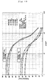
- FIG. 9 is a graph showing a result of measuring a vibrator current following the capacitance Cce when constants of each circuit constituent element according to the first embodiment shown in FIG. 1 are set as follows.
- Rc 330 ⁇ , and Cce and Cbe are variable.
- the capacitance Cbe between the base and the emitter is 20 pF, 43 pF, and 68 pF.
- the abscissa represents the capacitance Cce between the collector and the emitter, and the ordinate represents vibrator current. From FIG. 9 , it is clear that when the capacitance Cce between the collector and the emitter becomes 30 pF or above, the vibrator current decreases rapidly, and the vibrator current becomes smaller when the capacitance Cbe between the base and the emitter is smaller.
- FIG. 10 is a graph showing changes in the collector output voltage Vc and the emitter output voltage Ve respectively versus the capacitance Cce between the collector and the emitter when the capacitance Cbe between the base and the emitter is used as a parameter (20 pF, 68 pF, and 100 pF).
- the collector output voltage Vc and the emitter output voltage Ve are suppressed rapidly. Following this, the vibrator current is also suppressed rapidly.
- FIG. 11 is a graph showing changes in the vibrator current and the oscillation circuit current respectively versus the capacitance Cce between the collector and the emitter when the capacitance Cbe between the base and the emitter is used as a parameter of 20 pF and 68 pF according to the first embodiment shown in FIG. 1 . From FIG. 11 , it is clear that the oscillation circuit current changes little versus the suppression of the vibrator current. It is understood from this that the vibrator current is not suppressed because of the reduction in the gain due to the suppression of the base current and the collector current of the transistor TR 1 .
- FIG. 12 and FIG. 13 illustrate results of measuring negative resistance characteristics versus a change in frequency when the capacitance Cce between the collector and the emitter is used as a parameter (0 pF, 15 pF, and 51 pF) according to the first embodiment shown in FIG. 1 .
- the capacitance Cbe between the base and the emitter is 20 pF.
- the capacitance Cbe between the base and the emitter is 43 pF.
- FIG. 14 illustrates a relationship between the vibrator current and the capacitance Cbe between the base and the emitter and the capacitance Cce between the collector and the emitter respectively, when the negative resistance is at a maximum value in the oscillation frequency 10 MHz.
- a solid line 61 represents vibrator current characteristics according to the present invention.
- FIG. 15 illustrates a relationship between the capacitance Cbe between the base and the emitter and a capacitance Ceg between the emitter and the ground when the negative resistance is at a maximum value in the oscillation frequency 10 MHz, where the capacitance Cce between the collector and the emitter is used as a parameter (0 pF, 20 pF, 51 pF, and 100 pF).
- a solid line 63 represents characteristics according to the present invention.
- FIG. 16 illustrates negative resistance characteristics when transistors shown in FIG. 2 are connected in cascade. As is clear from FIG. 16 , when the capacitance Cce between the collector and the emitter is set to a suitable value in the cascade connection, the negative resistance increases like that in FIGS. 12 and 13 .
- FIG. 17 illustrates changes in the vibrator current and the oscillation circuit current versus the capacitance Cce between the collector and the emitter, when the capacitance Cbe between the base and the emitter is 20 pF in the cascade connection shown in FIG. 2 .
- the vibrator current is 170 ⁇ A
- the circuit current is 1.5 mA.
- the circuit current is 2.3 mA (maximum).
- FIG. 17 indicates that when a suitable value is selected for Cce, the vibrator current can be suppressed. This suppression is not attributable to the suppression of the circuit current.
- the collector and the emitter of the oscillation transistor are connected with a capacitor.
- the output is suppressed by a signal of a negative phase, and the base current is suppressed at the same time.
- the vibrator current can be decreased, and the negative resistance can be increased.
- the basic oscillation circuit is a Colpitts oscillator. Therefore, the circuit configuration is simple, and a stable oscillation can be achieved.
- the total gain is equivalent to that of the grounded-emitter circuit.
- the bandwidth can be secured up to the cut-off frequency of the grounded-base circuit. Therefore, an oscillator having excellent high-frequency characteristics can be obtained.
- this transistor by connecting the base of the second transistor to the ground via the capacitor, this transistor can be made as the grounded-emitter circuit. Therefore, a cascade circuit can be configured together with a transmission transistor.
- the bases of the oscillation amplifier transistor and the second transistor are biased at a predetermined potential respectively. Therefore, an oscillator having little waveform distortion can be obtained.
- the vibrator current can be decreased while securely carrying out oscillation.
Landscapes
- Oscillators With Electromechanical Resonators (AREA)
Abstract
Description
z=
|ix|=Ve/Z=Ve/[(r 1+r 2)2+{1/ω·(1/
where
- Z represents an impedance between the voltage supply Vcc end of the crystal oscillator and the ground,
- r1 and r2 represent resistors based on the parallel-to-series conversion shown in
FIG. 22 , - c1 and c2 represent capacitors based on the parallel-to-series conversion shown in
FIG. 22 , - Rπ represents an input resistance of the transistor in a parallel equivalent circuit shown in
FIG. 21 , - Cπ represents a junction capacitance of the transistor in the parallel equivalent circuit shown in
FIG. 21 , - Re represents emitter additional resistance of the transistor in the parallel equivalent circuit shown in
FIG. 21 , - Ce represents an emitter additional capacitor of the transistor in the parallel equivalent circuit shown in
FIG. 21 , - ω represents an angular frequency (=2πf)
- Ve represents a steady emitter output voltage,
- ix represents a vibrator current, and
- |ix| represents an effective value of the vibrator current.
i 1′=
|i 1′|=
i 1″=v 3/p 2 +q 2 {pr 2+q/ωc 3+j(
|i 1″|=v 3/p 2 +q 2×{(pr 2+q/ωc 2)2+(
|i|=|i 1′|+|
Claims (5)
Priority Applications (1)
| Application Number | Priority Date | Filing Date | Title |
|---|---|---|---|
| US10/676,400 US7009459B2 (en) | 2003-10-01 | 2003-10-01 | Piezoelectric oscillator having a non-inductive load with a collector-emitter capacitor |
Applications Claiming Priority (1)
| Application Number | Priority Date | Filing Date | Title |
|---|---|---|---|
| US10/676,400 US7009459B2 (en) | 2003-10-01 | 2003-10-01 | Piezoelectric oscillator having a non-inductive load with a collector-emitter capacitor |
Publications (2)
| Publication Number | Publication Date |
|---|---|
| US20050073372A1 US20050073372A1 (en) | 2005-04-07 |
| US7009459B2 true US7009459B2 (en) | 2006-03-07 |
Family
ID=34393578
Family Applications (1)
| Application Number | Title | Priority Date | Filing Date |
|---|---|---|---|
| US10/676,400 Expired - Fee Related US7009459B2 (en) | 2003-10-01 | 2003-10-01 | Piezoelectric oscillator having a non-inductive load with a collector-emitter capacitor |
Country Status (1)
| Country | Link |
|---|---|
| US (1) | US7009459B2 (en) |
Cited By (3)
| Publication number | Priority date | Publication date | Assignee | Title |
|---|---|---|---|---|
| US20060061427A1 (en) * | 2003-01-10 | 2006-03-23 | Toyo Communication Equipment Co., Ltd. | Piezoelectric oscillator |
| US20060208817A1 (en) * | 2005-03-15 | 2006-09-21 | Epson Toyocom Corporation | Piezoelectric oscillator |
| US20060270376A1 (en) * | 2001-10-22 | 2006-11-30 | Fujitsu Limited | Mixer circuit, receiver circuit, and frequency comparison circuit |
Families Citing this family (1)
| Publication number | Priority date | Publication date | Assignee | Title |
|---|---|---|---|---|
| JP2014175679A (en) * | 2013-03-06 | 2014-09-22 | Nippon Dempa Kogyo Co Ltd | Oscillator circuit |
Citations (5)
| Publication number | Priority date | Publication date | Assignee | Title |
|---|---|---|---|---|
| US4193046A (en) * | 1977-11-08 | 1980-03-11 | Kinsekisha Laboratory, Ltd. | Piezo-electric oscillators with automatic gain control |
| US5523722A (en) * | 1993-10-06 | 1996-06-04 | Kabushiki Kaisha Tokai Rika Denki Seisakusho | Saw oscillator with antenna |
| US5789990A (en) * | 1996-02-14 | 1998-08-04 | Rf Monolithics, Inc. | Feedback oscillator circuit using a saw resonator filter |
| US5920234A (en) * | 1995-05-24 | 1999-07-06 | Ut Automotive Dearborn, Inc. | Buffered oscillator transmitter arrangement for power specific applications having parasitic impedances |
| US20010043125A1 (en) * | 2000-05-16 | 2001-11-22 | Murata Manufacturing Co., Ltd. | Oscillator |
-
2003
- 2003-10-01 US US10/676,400 patent/US7009459B2/en not_active Expired - Fee Related
Patent Citations (5)
| Publication number | Priority date | Publication date | Assignee | Title |
|---|---|---|---|---|
| US4193046A (en) * | 1977-11-08 | 1980-03-11 | Kinsekisha Laboratory, Ltd. | Piezo-electric oscillators with automatic gain control |
| US5523722A (en) * | 1993-10-06 | 1996-06-04 | Kabushiki Kaisha Tokai Rika Denki Seisakusho | Saw oscillator with antenna |
| US5920234A (en) * | 1995-05-24 | 1999-07-06 | Ut Automotive Dearborn, Inc. | Buffered oscillator transmitter arrangement for power specific applications having parasitic impedances |
| US5789990A (en) * | 1996-02-14 | 1998-08-04 | Rf Monolithics, Inc. | Feedback oscillator circuit using a saw resonator filter |
| US20010043125A1 (en) * | 2000-05-16 | 2001-11-22 | Murata Manufacturing Co., Ltd. | Oscillator |
Cited By (4)
| Publication number | Priority date | Publication date | Assignee | Title |
|---|---|---|---|---|
| US20060270376A1 (en) * | 2001-10-22 | 2006-11-30 | Fujitsu Limited | Mixer circuit, receiver circuit, and frequency comparison circuit |
| US20060061427A1 (en) * | 2003-01-10 | 2006-03-23 | Toyo Communication Equipment Co., Ltd. | Piezoelectric oscillator |
| US7205856B2 (en) * | 2003-01-10 | 2007-04-17 | Toyo Communication Equipment Co., Ltd. | Piezoelectric oscillator |
| US20060208817A1 (en) * | 2005-03-15 | 2006-09-21 | Epson Toyocom Corporation | Piezoelectric oscillator |
Also Published As
| Publication number | Publication date |
|---|---|
| US20050073372A1 (en) | 2005-04-07 |
Similar Documents
| Publication | Publication Date | Title |
|---|---|---|
| JP2003078348A (en) | Voltage controlled oscillator and communication apparatus employing the same | |
| EP0767532B1 (en) | Oscillation circuit and oscillation method | |
| US6995623B2 (en) | Piezoelectric oscillator | |
| US6411170B2 (en) | Oscillation circuit | |
| US7009459B2 (en) | Piezoelectric oscillator having a non-inductive load with a collector-emitter capacitor | |
| EP1777808A1 (en) | High frequency Colpitts oscillation circuit | |
| US6043720A (en) | Oscillator frequency drift compensated by varying different biassing parameters | |
| US20040189412A1 (en) | Temperature compensated piezoelectric oscillator and electronic device using the same | |
| JP2643180B2 (en) | Monolithic integrated circuit | |
| US7109814B2 (en) | Piezoelectric oscillator | |
| US20040104783A1 (en) | High-frequency piezoelectric oscillator | |
| JP4066751B2 (en) | Piezoelectric oscillator | |
| US7205856B2 (en) | Piezoelectric oscillator | |
| JP3949482B2 (en) | Oscillator with temperature compensation function | |
| JPH09162641A (en) | Voltage control oscillator | |
| JP2001077626A (en) | Oscillator with buffer circuit | |
| JP2004104609A (en) | Temperature compensation type piezoelectric oscillator | |
| JP3387278B2 (en) | Temperature compensated piezoelectric oscillator | |
| JPH066594Y2 (en) | Overtone crystal oscillator circuit | |
| JPS6213841B2 (en) | ||
| JP2004266820A (en) | Piezoelectric oscillation circuit | |
| JPH0964641A (en) | Temperature compensated crystal oscillation device | |
| JP4190874B2 (en) | Piezoelectric oscillation circuit | |
| JPS6165607A (en) | Crystal oscillation circuit | |
| JPH06350336A (en) | Oscillator |
Legal Events
| Date | Code | Title | Description |
|---|---|---|---|
| AS | Assignment |
Owner name: TOYO COMMUNICATION EQUIPMENT CO., LTD., JAPAN Free format text: ASSIGNMENT OF ASSIGNORS INTEREST;ASSIGNORS:SATOH, TOMIO;MATSUOKA, JUN;OHSHIMA, TSUYOSHI;REEL/FRAME:015010/0916 Effective date: 20031215 |
|
| AS | Assignment |
Owner name: EPSON TOYOCOM CORPORATION, JAPAN Free format text: CHANGE OF NAME;ASSIGNOR:TOYO COMMUNICATION EQUIPMENT CO., LTD.;REEL/FRAME:020174/0556 Effective date: 20051003 |
|
| AS | Assignment |
Owner name: EPSON TOYOCOM CORPORATION, JAPAN Free format text: CHANGE OF ADDRESS;ASSIGNOR:EPSON TOYOCOM CORPORATION;REEL/FRAME:020431/0246 Effective date: 20060718 |
|
| FPAY | Fee payment |
Year of fee payment: 4 |
|
| FEPP | Fee payment procedure |
Free format text: PAYOR NUMBER ASSIGNED (ORIGINAL EVENT CODE: ASPN); ENTITY STATUS OF PATENT OWNER: LARGE ENTITY |
|
| AS | Assignment |
Owner name: SEIKO EPSON CORPORATION, JAPAN Free format text: ASSIGNMENT OF ASSIGNORS INTEREST;ASSIGNOR:EPSON TOYOCOM CORPORATION;REEL/FRAME:026717/0436 Effective date: 20110725 |
|
| FPAY | Fee payment |
Year of fee payment: 8 |
|
| FEPP | Fee payment procedure |
Free format text: MAINTENANCE FEE REMINDER MAILED (ORIGINAL EVENT CODE: REM.) |
|
| LAPS | Lapse for failure to pay maintenance fees |
Free format text: PATENT EXPIRED FOR FAILURE TO PAY MAINTENANCE FEES (ORIGINAL EVENT CODE: EXP.) |
|
| STCH | Information on status: patent discontinuation |
Free format text: PATENT EXPIRED DUE TO NONPAYMENT OF MAINTENANCE FEES UNDER 37 CFR 1.362 |
|
| FP | Lapsed due to failure to pay maintenance fee |
Effective date: 20180307 |