US6924171B2 - Bilayer wafer-level underfill - Google Patents
Bilayer wafer-level underfill Download PDFInfo
- Publication number
- US6924171B2 US6924171B2 US09/782,494 US78249401A US6924171B2 US 6924171 B2 US6924171 B2 US 6924171B2 US 78249401 A US78249401 A US 78249401A US 6924171 B2 US6924171 B2 US 6924171B2
- Authority
- US
- United States
- Prior art keywords
- polymeric material
- conductive bump
- forming
- wafer
- polymeric
- Prior art date
- Legal status (The legal status is an assumption and is not a legal conclusion. Google has not performed a legal analysis and makes no representation as to the accuracy of the status listed.)
- Expired - Lifetime
Links
Images


Classifications
-
- H—ELECTRICITY
- H10—SEMICONDUCTOR DEVICES; ELECTRIC SOLID-STATE DEVICES NOT OTHERWISE PROVIDED FOR
- H10W—GENERIC PACKAGES, INTERCONNECTIONS, CONNECTORS OR OTHER CONSTRUCTIONAL DETAILS OF DEVICES COVERED BY CLASS H10
- H10W72/00—Interconnections or connectors in packages
- H10W72/01—Manufacture or treatment
- H10W72/0198—Manufacture or treatment batch processes
-
- H—ELECTRICITY
- H10—SEMICONDUCTOR DEVICES; ELECTRIC SOLID-STATE DEVICES NOT OTHERWISE PROVIDED FOR
- H10W—GENERIC PACKAGES, INTERCONNECTIONS, CONNECTORS OR OTHER CONSTRUCTIONAL DETAILS OF DEVICES COVERED BY CLASS H10
- H10W74/00—Encapsulations, e.g. protective coatings
- H10W74/01—Manufacture or treatment
- H10W74/012—Manufacture or treatment of encapsulations on active surfaces of flip-chip devices, e.g. forming underfills
-
- H—ELECTRICITY
- H10—SEMICONDUCTOR DEVICES; ELECTRIC SOLID-STATE DEVICES NOT OTHERWISE PROVIDED FOR
- H10W—GENERIC PACKAGES, INTERCONNECTIONS, CONNECTORS OR OTHER CONSTRUCTIONAL DETAILS OF DEVICES COVERED BY CLASS H10
- H10W74/00—Encapsulations, e.g. protective coatings
- H10W74/10—Encapsulations, e.g. protective coatings characterised by their shape or disposition
- H10W74/15—Encapsulations, e.g. protective coatings characterised by their shape or disposition on active surfaces of flip-chip devices, e.g. underfills
-
- H—ELECTRICITY
- H10—SEMICONDUCTOR DEVICES; ELECTRIC SOLID-STATE DEVICES NOT OTHERWISE PROVIDED FOR
- H10W—GENERIC PACKAGES, INTERCONNECTIONS, CONNECTORS OR OTHER CONSTRUCTIONAL DETAILS OF DEVICES COVERED BY CLASS H10
- H10W74/00—Encapsulations, e.g. protective coatings
- H10W74/40—Encapsulations, e.g. protective coatings characterised by their materials
- H10W74/47—Encapsulations, e.g. protective coatings characterised by their materials comprising organic materials, e.g. plastics or resins
- H10W74/473—Encapsulations, e.g. protective coatings characterised by their materials comprising organic materials, e.g. plastics or resins containing a filler
-
- H—ELECTRICITY
- H10—SEMICONDUCTOR DEVICES; ELECTRIC SOLID-STATE DEVICES NOT OTHERWISE PROVIDED FOR
- H10W—GENERIC PACKAGES, INTERCONNECTIONS, CONNECTORS OR OTHER CONSTRUCTIONAL DETAILS OF DEVICES COVERED BY CLASS H10
- H10W72/00—Interconnections or connectors in packages
- H10W72/01—Manufacture or treatment
- H10W72/012—Manufacture or treatment of bump connectors, dummy bumps or thermal bumps
- H10W72/01251—Changing the shapes of bumps
- H10W72/01255—Changing the shapes of bumps by using masks
-
- H—ELECTRICITY
- H10—SEMICONDUCTOR DEVICES; ELECTRIC SOLID-STATE DEVICES NOT OTHERWISE PROVIDED FOR
- H10W—GENERIC PACKAGES, INTERCONNECTIONS, CONNECTORS OR OTHER CONSTRUCTIONAL DETAILS OF DEVICES COVERED BY CLASS H10
- H10W72/00—Interconnections or connectors in packages
- H10W72/01—Manufacture or treatment
- H10W72/013—Manufacture or treatment of die-attach connectors
- H10W72/01331—Manufacture or treatment of die-attach connectors using blanket deposition
-
- H—ELECTRICITY
- H10—SEMICONDUCTOR DEVICES; ELECTRIC SOLID-STATE DEVICES NOT OTHERWISE PROVIDED FOR
- H10W—GENERIC PACKAGES, INTERCONNECTIONS, CONNECTORS OR OTHER CONSTRUCTIONAL DETAILS OF DEVICES COVERED BY CLASS H10
- H10W72/00—Interconnections or connectors in packages
- H10W72/071—Connecting or disconnecting
- H10W72/073—Connecting or disconnecting of die-attach connectors
-
- H—ELECTRICITY
- H10—SEMICONDUCTOR DEVICES; ELECTRIC SOLID-STATE DEVICES NOT OTHERWISE PROVIDED FOR
- H10W—GENERIC PACKAGES, INTERCONNECTIONS, CONNECTORS OR OTHER CONSTRUCTIONAL DETAILS OF DEVICES COVERED BY CLASS H10
- H10W72/00—Interconnections or connectors in packages
- H10W72/20—Bump connectors, e.g. solder bumps or copper pillars; Dummy bumps; Thermal bumps
- H10W72/251—Materials
- H10W72/252—Materials comprising solid metals or solid metalloids, e.g. PbSn, Ag or Cu
-
- H—ELECTRICITY
- H10—SEMICONDUCTOR DEVICES; ELECTRIC SOLID-STATE DEVICES NOT OTHERWISE PROVIDED FOR
- H10W—GENERIC PACKAGES, INTERCONNECTIONS, CONNECTORS OR OTHER CONSTRUCTIONAL DETAILS OF DEVICES COVERED BY CLASS H10
- H10W72/00—Interconnections or connectors in packages
- H10W72/30—Die-attach connectors
- H10W72/351—Materials of die-attach connectors
- H10W72/352—Materials of die-attach connectors comprising metals or metalloids, e.g. solders
-
- H—ELECTRICITY
- H10—SEMICONDUCTOR DEVICES; ELECTRIC SOLID-STATE DEVICES NOT OTHERWISE PROVIDED FOR
- H10W—GENERIC PACKAGES, INTERCONNECTIONS, CONNECTORS OR OTHER CONSTRUCTIONAL DETAILS OF DEVICES COVERED BY CLASS H10
- H10W72/00—Interconnections or connectors in packages
- H10W72/30—Die-attach connectors
- H10W72/351—Materials of die-attach connectors
- H10W72/353—Materials of die-attach connectors not comprising solid metals or solid metalloids, e.g. ceramics
- H10W72/354—Materials of die-attach connectors not comprising solid metals or solid metalloids, e.g. ceramics comprising polymers
-
- H—ELECTRICITY
- H10—SEMICONDUCTOR DEVICES; ELECTRIC SOLID-STATE DEVICES NOT OTHERWISE PROVIDED FOR
- H10W—GENERIC PACKAGES, INTERCONNECTIONS, CONNECTORS OR OTHER CONSTRUCTIONAL DETAILS OF DEVICES COVERED BY CLASS H10
- H10W72/00—Interconnections or connectors in packages
- H10W72/851—Dispositions of multiple connectors or interconnections
- H10W72/853—On the same surface
- H10W72/856—Bump connectors and die-attach connectors
-
- H—ELECTRICITY
- H10—SEMICONDUCTOR DEVICES; ELECTRIC SOLID-STATE DEVICES NOT OTHERWISE PROVIDED FOR
- H10W—GENERIC PACKAGES, INTERCONNECTIONS, CONNECTORS OR OTHER CONSTRUCTIONAL DETAILS OF DEVICES COVERED BY CLASS H10
- H10W72/00—Interconnections or connectors in packages
- H10W72/90—Bond pads, in general
- H10W72/941—Dispositions of bond pads
- H10W72/9415—Dispositions of bond pads relative to the surface, e.g. recessed, protruding
-
- H—ELECTRICITY
- H10—SEMICONDUCTOR DEVICES; ELECTRIC SOLID-STATE DEVICES NOT OTHERWISE PROVIDED FOR
- H10W—GENERIC PACKAGES, INTERCONNECTIONS, CONNECTORS OR OTHER CONSTRUCTIONAL DETAILS OF DEVICES COVERED BY CLASS H10
- H10W90/00—Package configurations
- H10W90/701—Package configurations characterised by the relative positions of pads or connectors relative to package parts
- H10W90/721—Package configurations characterised by the relative positions of pads or connectors relative to package parts of bump connectors
- H10W90/724—Package configurations characterised by the relative positions of pads or connectors relative to package parts of bump connectors between a chip and a stacked insulating package substrate, interposer or RDL
Definitions
- the present invention relates to microelectronic packaging, and more particularly to a microelectronic interconnect structure and to a method of fabricating the same.
- the inventive method which utilizes a bilayer polymeric underfill eliminates separate underfill steps that are typically required in prior art methods of fabricating microelectronic interconnect structures.
- Flip chip technology has grown rapidly in recent years as a means of decreasing the chip footprint while simultaneously increasing the number of possible I/O's. This is because flip chip technology takes advantage of the chip area for I/O's instead of just the chip periphery as does wire bonding.
- Various methods exist for solder bumping wafers such as evaporation, plating, solder paste screening and more recently, injection molding solder, i.e., IMS.
- the wafers are typically thereafter diced into separate chips.
- direct chip attach i.e., DCA
- silicon chips are bonded directly to a laminate substrate. Since there is significant mismatch of CTE (coefficient of thermal expansion) between silicon and laminate materials, these chips are thereafter underfilled; Underfilling greatly increases the fatigue life of the solder bumps.
- underfilling is associated with several manufacturing problems.
- the process is somewhat slow. This is due to the typical dispensing method of applying the liquid underfill along at least two sides of the chip and letting capillary action pull the liquid completely under the chip.
- incomplete underfills may occur. Since it is difficult to determine underfill uniformity, this could lead to excess mechanical stresses on affected bumps. This, in turn, leads to shortened fatigue life for the affected chip.
- many flip chip packages are 100% inspected by scanning acoustic microscopy, an expensive process.
- underfilling is a packaging-processing step which must be done on each flip chip. Ideally, this step should be done on the wafer to accelerate the path from wafer to packaged chip.
- the underfill if the underfill is applied to a wafer already populated with solder bumps, the filler particles in the underfill will impede good wetting of the solder to the chip carrier pads. Without filler, the underfill cannot perform its function of reinforcing the solder joints because unfilled polymeric materials commonly have coefficients of thermal expansion much higher than that of solder.
- solder bumps cannot be applied after the underfill is applied because then the B-staged underfill will be subjected to solder reflow temperatures during which it will liquefy and cure further.
- One object of the present invention is to provide a method of fabricating a microelectronic interconnect structure that addresses the limitations of flip chip packaging with underfill applied at the package level.
- a further object of the present invention is to provide a method of fabricating a microelectronic interconnect structure that is simple and easy to implement in current packaging technology.
- a yet further object of the present invention is to provide a method of fabricating a microelectronic interconnect structure that avoids the processing problems associated with single-layer wafer-level underfills.
- one method of the present invention comprises the steps of:
- a second method is also provided wherein the initial semiconductor wafer includes conductive bump material previously formed thereon.
- the second method of the present invention comprises the steps of:
- microelectronic interconnect structure which is fabricated using the above-mentioned processing steps.
- inventive microelectronic interconnect structure comprises:
- FIGS. 1A-H are cross-sectional views illustrating the inventive microelectronic interconnect structure through various processing steps of the present invention.
- FIGS. 2A-D are cross-sectional views illustrating the inventive microelectronic interconnect structure through alternative processing steps of the present invention.
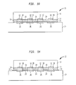
- FIG. 1A illustrates an initial structure that can be employed in the present invention.
- the initial structure shown in FIG. 1A comprises semiconductor wafer 10 having interconnect pads 12 formed on predetermined portions of the wafer.
- the structure shown in FIG. 1A is comprised of conventional materials well known to those skilled in the art and conventional processing steps are used in fabricating the same.
- semiconductor wafer 10 is comprised of a semiconducting material including, but not limited to: Si, Ge, SiGe, GaAs, InAs, InP and all other II/V compound semiconductors.
- the wafer may also be composed of a layered semiconductor such as Si/SiGe, Si/Si or silicon-on-insulators (SOIs).
- SOIs silicon-on-insulators
- the wafer includes various semiconductor devices (not shown in the drawings) that are formed within or on the wafer.
- Illustrative examples of some types of devices that may be present include, but are not limited to: transistors, capacitors, memory cells, drivers, I/O circuitry, charge pumps and other like devices.
- the wafer may include any combination of the aforementioned devices.
- the wafer is fabricated using conventional processes well known to those skilled in the art which may vary depending on the types of devices present therein. For example, conventional complementary metal oxide semiconductor (CMOS) processing steps may be used in forming the transistors and back-end-of-the-line (BEOL) processes may be used in forming the interconnect pads on the surface of the wafer. Although not depicted in the drawings, the wafer contains the appropriate ball-limiting metallurgy (BLM) covering the pads which will receive the conductive bump material.
- CMOS complementary metal oxide semiconductor
- BEOL back-end-of-the-line
- the wafer contains the appropriate ball-limiting metallurgy (BLM) covering the pads which will receive the conductive bump material.
- BBM ball-limiting metallurgy
- FIG. 1B shows a structure after application of first polymeric material 14 to the wafer front side containing the interconnect pads.
- the first polymeric material is formed using conventional deposition processes well known to those skilled in the art including: spin coating, dip coating, brushing, chemical vapor deposition (CVD), plasma-assisted CVD, sputtering, chemical solution deposition and other like deposition processes. Of these various deposition processes, it is preferred to form the first polymeric layer by spin coating.
- the first polymeric material may be hot baked and cured using conventional conditions prior to proceeding to the next step of the present invention. Alternatively, the first polymeric material may be patterned before the final cure utilizing conventional processes well known in the art.
- the first polymeric material employed in the present invention is composed of a dielectric passivating material such as polyimides, polyamides, Si-containing polymers, parylene polymers, polybenzocyclobutane, epoxies and other like dielectric passivating materials.
- a dielectric passivating material such as polyimides, polyamides, Si-containing polymers, parylene polymers, polybenzocyclobutane, epoxies and other like dielectric passivating materials.
- first polymeric material 14 be composed of polyimides or an epoxy.
- the thickness of the first polymeric material may vary, however, it should be thicker than the current passivation layers that are employed in the prior art. Typically, the first polymeric material has a final thickness of from about 25 to about 100 microns.
- the first polymeric material may optionally include an inorganic filler therein which substantially reduces the thermal coefficient of expansion of the material.
- inorganic fillers that may be present in the first polymeric material include: silica, fumed silica, alumina, titanium dioxide, glass fibers and other like inorganic fillers. Mixtures of these inorganic fillers are also contemplated herein.
- the inorganic fillers are typically present in said first polymeric material in an amount of from about 10 to about 80 wt. %, with an amount of from about 50 to about 70 wt. % being more highly preferred.
- the structure shown in FIG. 1B is subjected to any conventional patterning process such as laser etching or lithography and etching which forms openings 16 in the structure that expose pads 12 .
- the patterned structure is shown, for example, in FIG. 1 C.
- the lithography step employed in forming the structure illustrated in FIG. 1C includes application of a photoresist, exposing the photoresist to a pattern of radiation and developing the pattern using a conventional resist developer.
- the etching step which forms the openings in the first polymeric material that expose the underlying interconnect pads includes dry etching processes such as laser ablation, reactive-ion etching (RIE), plasma etching, and ion beam etching as well as wet etching using a chemical etchant that has a high selectivity to the polymeric material.
- dry etching processes such as laser ablation, reactive-ion etching (RIE), plasma etching, and ion beam etching as well as wet etching using a chemical etchant that has a high selectivity to the polymeric material.
- FIG. 1D shows a structure wherein conductive bump material 18 is formed on exposed surfaces of pads 12 using said patterned first polymeric material as a mask.
- the conductive bump material that is employed in the present invention includes conventional conductive materials which are capable of forming a bond to the underlying pads.
- conductive bump materials include, but are not limited to: Sn—Ag, Sn—Ag—Cu, and other lead-free solders such as Sn—Ag—Bi and conventional solders such as Sn—Pb, and other like materials.
- a highly preferred conductive bump material employed in the present invention is Sn—Pb solder.
- the conductive bump material may be applied in the openings using conventional techniques that are well known to those skilled in the art.
- an injection molded solder (IMS) process which scans a head containing molten solder over the wafer and fills the cavities, may be employed in the present invention. After filling the openings with solder, the wafer is cooled and the solder solidifies.
- the first polymeric material also serves as the major portion of the underfill as will be seen in the drawings to follow.
- the present invention also contemplates the use of evaporation, plating and paste screening as means for forming conductive bump material 18 on pads 12 .
- a thin layer of second polymeric material 20 is applied uniformly over the wafer including first polymeric material 14 and conductive bumps 18 , See FIG. 1 E.
- the second polymeric material which includes a flux material and an adhesive, is applied using one of the above mentioned deposition processes that are used in forming the first polymeric material. For example, a spin coating or similar process may be used.
- the thickness of the second polymeric material may vary, the second polymeric material should have a thickness that is less than the first polymeric material. Typically, in the present invention, the second polymeric material has a thickness of from about 1 to about 10 micron.
- thermoplastics thermosets such as epoxies and polyimides
- other adhesives epoxies
- the structure is partially cured so as to harden the second polymeric material.
- This curing step may be carried out using conditions that are capable of hardening the second polymeric material into a partially cured state (B-stage).
- FIG. 1F shows diced chip 22 containing in effect everything required to bond and underfill it to an external substrate such as a laminate substrate.
- FIG. 1G shows the flipped chip being aligned and placed on external substrate 24 .
- External substrate 24 which includes receiving pads 26 is composed of a conventional substrate such as a laminate substrate, a chip carrier, a printed circuit card or board. As shown, the conductive bump filled openings align to the receiving pads on the external substrate.
- the diced chip is bonded to the external substrate using any well known bonding process which is capable of heating the conductive bump material to its reflow temperature.
- bonding occurs at a temperature of from about 180° to about 260° C. for a time period of from about 1 to about 10 minutes.
- this heating step serves the following two functions: First, it activates the fluxing agent in the second polymeric material thus allowing the conductive bump material to penetrate through it and wet (metallurgically bond) to the pad on the external substrate. Secondly, it activates the adhesive in the second polymeric material which mechanically bonds the chip to the external substrate. Since the second polymeric layer is thin (typically below 10 microns) compared to the first polymeric material which serves as the conductive bump mask, there is very little conductive bump volume needed to penetrate through it. Also, during this heating step, the second polymeric material thins still further as it bonds to the external substrate. Thus most of the conductive bump volume stays within the openings and is surrounded by the walls of each opening. The net result is the same as for conventional underfills, i.e., solder joints are completely surrounded and reinforced by the underfill.
- FIG. 1H shows the inventive interconnect structure of the present invention.
- the inventive structure comprises chip 22 bonded to external substrate 24 through conductive bump material 18 .
- the conductive bump material is surrounded by a bilayer that comprises first polymeric material 14 and second polymeric material 20 .
- FIGS. 2A-D show semiconductor wafer 10 having conductive bump material 18 formed on predetermined portions of the wafer that include interconnect pads. The interconnect pads are not shown in these drawings, but nevertheless are present on the surface of wafer 10 .
- FIG. 2B shows a structure which includes first polymeric material 14 formed on the bumped wafer. Note that the thickness of the first polymeric material, in this embodiment, should be sufficient to at least cover every bump present on the wafer.
- the first polymeric material is then thinned by utilizing a conventional polishing process such as chemical-mechanical polishing (CMP) or etching to expose a top surface of every bump, See FIG. 2C.
- CMP chemical-mechanical polishing
- a thin layer of second polymeric material 20 is then applied on the thinned structure of FIG. 2C to cover every bump; See FIG. 2D , and partially cured.
- the wafer is ready for dicing into chips which can be flip chip bonded to the external substrate.
- the structure shown in FIG. 2D is then subjected to the processes that are described above in forming the structures shown in FIGS. 1F-H .
Landscapes
- Wire Bonding (AREA)
Abstract
Description
- (a) forming a first polymeric material on a surface of a semiconductor wafer having interconnect pads disposed thereon;
- (b) patterning said first polymeric material to provide openings that expose said interconnect pads;
- (c) forming conductive bump material in said openings;
- (d) forming a second polymeric material over said first polymeric material and said conductive bump material;
- (e) dicing said semiconductor wafer into individual chips; and
- (f) bonding at least one of said individual chips to an external substrate, wherein during said bonding said conductive bump material penetrates said second polymeric material and contacts a surface of said external substrate.
- (a) forming a first polymeric material on a surface of a semiconductor wafer having conductive bump material disposed on portions thereof;
- (b) removing a portion of said first polymeric material so as to expose top surfaces of said conductive bump material;
- (c) forming a second polymeric material on said first polymeric material and said exposed top surfaces of said conductive bump material;
- (d) dicing said semiconductor wafer into individual chips; and
- (e) bonding at least one of said individual chips to an external substrate, wherein during said bonding said conductive bump material penetrates said second polymeric material and contacts a surface of said external substrate.
- a semiconductor chip having a surface wherein conductive bump material is disposed on portions thereof;
- a bilayer comprising a first polymeric material and a second polymeric material abutting said conductive bump material; and
- an external substrate bonded to said semiconductor chip by said conductive bump material.
Claims (22)
Priority Applications (1)
| Application Number | Priority Date | Filing Date | Title |
|---|---|---|---|
| US09/782,494 US6924171B2 (en) | 2001-02-13 | 2001-02-13 | Bilayer wafer-level underfill |
Applications Claiming Priority (1)
| Application Number | Priority Date | Filing Date | Title |
|---|---|---|---|
| US09/782,494 US6924171B2 (en) | 2001-02-13 | 2001-02-13 | Bilayer wafer-level underfill |
Publications (2)
| Publication Number | Publication Date |
|---|---|
| US20020109228A1 US20020109228A1 (en) | 2002-08-15 |
| US6924171B2 true US6924171B2 (en) | 2005-08-02 |
Family
ID=25126221
Family Applications (1)
| Application Number | Title | Priority Date | Filing Date |
|---|---|---|---|
| US09/782,494 Expired - Lifetime US6924171B2 (en) | 2001-02-13 | 2001-02-13 | Bilayer wafer-level underfill |
Country Status (1)
| Country | Link |
|---|---|
| US (1) | US6924171B2 (en) |
Cited By (29)
| Publication number | Priority date | Publication date | Assignee | Title |
|---|---|---|---|---|
| US20040219716A1 (en) * | 2002-11-13 | 2004-11-04 | Tessera, Inc. | Microelectronic assemblies having low profile connections |
| US20060003569A1 (en) * | 2002-07-08 | 2006-01-05 | Farnworth Warren M | Semiconductor devices with permanent polymer stencil and method for manufacturing the same |
| US20060046346A1 (en) * | 2004-09-01 | 2006-03-02 | Benson Peter A | Methods for packaging microfeature devices and microfeature devices formed by such methods |
| US20060068521A1 (en) * | 2004-09-29 | 2006-03-30 | Song-Hua Shi | Method of fabricating microelectronic package using no-flow underfill technology and microelectronic package formed according to the method |
| US20060097377A1 (en) * | 2004-11-09 | 2006-05-11 | Han-Shin Youn | Flip chip bonding structure using non-conductive adhesive and related fabrication method |
| US20060186518A1 (en) * | 2005-02-23 | 2006-08-24 | Kevin Wu | Module card structure |
| US20060211171A1 (en) * | 2005-03-18 | 2006-09-21 | Tummala Rao O | Underfill on substrate process and ultra-fine pitch, low standoff chip-to-package interconnections produced thereby |
| US20060289966A1 (en) * | 2005-06-22 | 2006-12-28 | Dani Ashay A | Silicon wafer with non-soluble protective coating |
| US20060289607A1 (en) * | 2005-06-28 | 2006-12-28 | Buchwalter Stephen L | Composite solder transfer moldplate structure and method of making same |
| US20070063325A1 (en) * | 2005-09-22 | 2007-03-22 | Chun-Hung Lin | Chip package structure and bumping process |
| US20070066048A1 (en) * | 2004-09-01 | 2007-03-22 | Benson Peter A | Method for creating electrically conductive elements for semiconductor device structures using laser ablation processes and methods of fabricating semiconductor device assemblies |
| US20080039608A1 (en) * | 2006-08-11 | 2008-02-14 | General Electric Company | Oxetane composition, associated method and article |
| US20080039542A1 (en) * | 2006-08-11 | 2008-02-14 | General Electric Company | Composition and associated method |
| US20080039560A1 (en) * | 2006-08-11 | 2008-02-14 | General Electric Company | Syneretic composition, associated method and article |
| US20080121845A1 (en) * | 2006-08-11 | 2008-05-29 | General Electric Company | Oxetane composition, associated method and article |
| US20080315424A1 (en) * | 2001-03-30 | 2008-12-25 | Megica Corporation | Structure and manufactruing method of chip scale package |
| US20090102070A1 (en) * | 2007-10-22 | 2009-04-23 | International Business Machines Corporation | Alignment Marks on the Edge of Wafers and Methods for Same |
| US20090108472A1 (en) * | 2007-10-29 | 2009-04-30 | International Business Machines Corporation | Wafer-level underfill process using over-bump-applied resin |
| US20090169886A1 (en) * | 2007-12-31 | 2009-07-02 | International Business Machines Corporation | Negative coefficient thermal expansion engineered particles for composite fabrication |
| US20090251698A1 (en) * | 2008-04-02 | 2009-10-08 | Claudius Feger | Method and system for collecting alignment data from coated chips or wafers |
| EP2141738A2 (en) | 2008-07-01 | 2010-01-06 | International Business Machines Corporation | Chip-level underfill process and structures |
| US20100129961A1 (en) * | 2008-11-25 | 2010-05-27 | International Business Machines Corporation | Multi chip stacking with reliable joining |
| US20110229822A1 (en) * | 2008-11-25 | 2011-09-22 | Stapleton Russell A | Methods for protecting a die surface with photocurable materials |
| US20130256857A1 (en) * | 2012-03-27 | 2013-10-03 | Infineon Technologies Ag | Semiconductor Packages and Methods of Formation Thereof |
| CN104008983A (en) * | 2014-05-04 | 2014-08-27 | 清华大学 | Metal protruding point manufacturing method |
| US9093448B2 (en) | 2008-11-25 | 2015-07-28 | Lord Corporation | Methods for protecting a die surface with photocurable materials |
| US9461007B2 (en) | 2014-07-11 | 2016-10-04 | Samsung Electronics Co., Ltd. | Wafer-to-wafer bonding structure |
| US9929080B2 (en) * | 2004-11-15 | 2018-03-27 | Intel Corporation | Forming a stress compensation layer and structures formed thereby |
| CN110544639A (en) * | 2019-08-23 | 2019-12-06 | 深圳宏芯宇电子股份有限公司 | Integrated circuit crystal grain mounting method and semiconductor device |
Families Citing this family (22)
| Publication number | Priority date | Publication date | Assignee | Title |
|---|---|---|---|---|
| US6352881B1 (en) * | 1999-07-22 | 2002-03-05 | National Semiconductor Corporation | Method and apparatus for forming an underfill adhesive layer |
| US6710454B1 (en) * | 2000-02-16 | 2004-03-23 | Micron Technology, Inc. | Adhesive layer for an electronic apparatus having multiple semiconductor devices |
| JP2002299378A (en) * | 2001-03-30 | 2002-10-11 | Lintec Corp | Adhesive sheet with conductor, semiconductor device manufacturing method and semiconductor device |
| US6660560B2 (en) * | 2001-09-10 | 2003-12-09 | Delphi Technologies, Inc. | No-flow underfill material and underfill method for flip chip devices |
| US7423337B1 (en) | 2002-08-19 | 2008-09-09 | National Semiconductor Corporation | Integrated circuit device package having a support coating for improved reliability during temperature cycling |
| TWI244129B (en) * | 2002-10-25 | 2005-11-21 | Via Tech Inc | Bonding column process |
| US7301222B1 (en) | 2003-02-12 | 2007-11-27 | National Semiconductor Corporation | Apparatus for forming a pre-applied underfill adhesive layer for semiconductor wafer level chip-scale packages |
| US6946384B2 (en) * | 2003-06-06 | 2005-09-20 | Intel Corporation | Stacked device underfill and a method of fabrication |
| US7320928B2 (en) * | 2003-06-20 | 2008-01-22 | Intel Corporation | Method of forming a stacked device filler |
| US20050212105A1 (en) * | 2004-03-23 | 2005-09-29 | Walk Michael J | Integrated circuit die and substrate coupling |
| US7282375B1 (en) | 2004-04-14 | 2007-10-16 | National Semiconductor Corporation | Wafer level package design that facilitates trimming and testing |
| TWI230989B (en) * | 2004-05-05 | 2005-04-11 | Megic Corp | Chip bonding method |
| US7067350B1 (en) * | 2005-01-31 | 2006-06-27 | Taiwan Semiconductor Manufacturing Company, Ltd. | Method of manufacturing a semiconductor device using electrical contacts formed in an isolation layer |
| US7410090B2 (en) * | 2006-04-21 | 2008-08-12 | International Business Machines Corporation | Conductive bonding material fill techniques |
| US7573138B2 (en) * | 2006-11-30 | 2009-08-11 | Taiwan Semiconductor Manufacturing Co., Ltd. | Stress decoupling structures for flip-chip assembly |
| US9314864B2 (en) | 2007-07-09 | 2016-04-19 | International Business Machines Corporation | C4NP compliant solder fill head seals |
| JP5004351B2 (en) * | 2007-11-30 | 2012-08-22 | 信越化学工業株式会社 | Manufacturing method of semiconductor device |
| US7931187B2 (en) * | 2008-11-12 | 2011-04-26 | International Business Machines Corporation | Injection molded solder method for forming solder bumps on substrates |
| US20110115099A1 (en) * | 2009-05-14 | 2011-05-19 | Vertical Circuits, Inc. | Flip-chip underfill |
| KR101677739B1 (en) | 2010-09-29 | 2016-11-21 | 삼성전자주식회사 | package for semiconductor device and manufacturing method of the same |
| JP2012124244A (en) * | 2010-12-07 | 2012-06-28 | Sony Chemical & Information Device Corp | Mounting method of semiconductor element and mounting body |
| EP3433876B1 (en) * | 2016-03-24 | 2023-09-13 | Siltectra GmbH | A splitting method |
Citations (17)
| Publication number | Priority date | Publication date | Assignee | Title |
|---|---|---|---|---|
| US3943623A (en) * | 1974-08-23 | 1976-03-16 | Nitto Electric Industrial Co., Ltd. | Hollow cavity package electronic unit |
| US4681654A (en) * | 1986-05-21 | 1987-07-21 | International Business Machines Corporation | Flexible film semiconductor chip carrier |
| US5153986A (en) * | 1991-07-17 | 1992-10-13 | International Business Machines | Method for fabricating metal core layers for a multi-layer circuit board |
| US5319244A (en) * | 1991-12-13 | 1994-06-07 | International Business Machines Corporation | Triazine thin film adhesives |
| US5895229A (en) * | 1997-05-19 | 1999-04-20 | Motorola, Inc. | Microelectronic package including a polymer encapsulated die, and method for forming same |
| US5909634A (en) * | 1996-12-20 | 1999-06-01 | Texas Instruments | Method and apparatus for forming solder on a substrate |
| US5930598A (en) * | 1996-05-01 | 1999-07-27 | Motorola, Inc. | Microelectronic assembly including a decomposable encapsulant, and method for forming and reworking same |
| US5975408A (en) * | 1997-10-23 | 1999-11-02 | Lucent Technologies Inc. | Solder bonding of electrical components |
| US6228678B1 (en) * | 1998-04-27 | 2001-05-08 | Fry's Metals, Inc. | Flip chip with integrated mask and underfill |
| US6346296B1 (en) * | 1999-09-14 | 2002-02-12 | Alliedsignal Inc. | Highly stable packaging substrates |
| US6372544B1 (en) * | 2000-06-23 | 2002-04-16 | Advanced Micro Devices, Inc. | Method to reduce occurrences of fillet cracking in flip-chip underfill |
| US6410415B1 (en) * | 1999-03-23 | 2002-06-25 | Polymer Flip Chip Corporation | Flip chip mounting technique |
| US20020105092A1 (en) * | 2001-02-02 | 2002-08-08 | Coyle Anthony L. | Flip chip semiconductor device in a molded chip scale package (CSP) and method of assembly |
| US6506681B2 (en) * | 2000-12-06 | 2003-01-14 | Micron Technology, Inc. | Thin flip—chip method |
| US20030199160A1 (en) * | 1996-05-21 | 2003-10-23 | Farnworth Warren M | Use of palladium in IC manufacturing with conductive polymer bump |
| US6656750B1 (en) * | 1999-04-29 | 2003-12-02 | International Business Machines Corporation | Method for testing chips on flat solder bumps |
| US6774493B2 (en) * | 1997-07-21 | 2004-08-10 | M. A. Capote | Semiconductor flip-chip package and method for the fabrication thereof |
-
2001
- 2001-02-13 US US09/782,494 patent/US6924171B2/en not_active Expired - Lifetime
Patent Citations (17)
| Publication number | Priority date | Publication date | Assignee | Title |
|---|---|---|---|---|
| US3943623A (en) * | 1974-08-23 | 1976-03-16 | Nitto Electric Industrial Co., Ltd. | Hollow cavity package electronic unit |
| US4681654A (en) * | 1986-05-21 | 1987-07-21 | International Business Machines Corporation | Flexible film semiconductor chip carrier |
| US5153986A (en) * | 1991-07-17 | 1992-10-13 | International Business Machines | Method for fabricating metal core layers for a multi-layer circuit board |
| US5319244A (en) * | 1991-12-13 | 1994-06-07 | International Business Machines Corporation | Triazine thin film adhesives |
| US5930598A (en) * | 1996-05-01 | 1999-07-27 | Motorola, Inc. | Microelectronic assembly including a decomposable encapsulant, and method for forming and reworking same |
| US20030199160A1 (en) * | 1996-05-21 | 2003-10-23 | Farnworth Warren M | Use of palladium in IC manufacturing with conductive polymer bump |
| US5909634A (en) * | 1996-12-20 | 1999-06-01 | Texas Instruments | Method and apparatus for forming solder on a substrate |
| US5895229A (en) * | 1997-05-19 | 1999-04-20 | Motorola, Inc. | Microelectronic package including a polymer encapsulated die, and method for forming same |
| US6774493B2 (en) * | 1997-07-21 | 2004-08-10 | M. A. Capote | Semiconductor flip-chip package and method for the fabrication thereof |
| US5975408A (en) * | 1997-10-23 | 1999-11-02 | Lucent Technologies Inc. | Solder bonding of electrical components |
| US6228678B1 (en) * | 1998-04-27 | 2001-05-08 | Fry's Metals, Inc. | Flip chip with integrated mask and underfill |
| US6410415B1 (en) * | 1999-03-23 | 2002-06-25 | Polymer Flip Chip Corporation | Flip chip mounting technique |
| US6656750B1 (en) * | 1999-04-29 | 2003-12-02 | International Business Machines Corporation | Method for testing chips on flat solder bumps |
| US6346296B1 (en) * | 1999-09-14 | 2002-02-12 | Alliedsignal Inc. | Highly stable packaging substrates |
| US6372544B1 (en) * | 2000-06-23 | 2002-04-16 | Advanced Micro Devices, Inc. | Method to reduce occurrences of fillet cracking in flip-chip underfill |
| US6506681B2 (en) * | 2000-12-06 | 2003-01-14 | Micron Technology, Inc. | Thin flip—chip method |
| US20020105092A1 (en) * | 2001-02-02 | 2002-08-08 | Coyle Anthony L. | Flip chip semiconductor device in a molded chip scale package (CSP) and method of assembly |
Cited By (51)
| Publication number | Priority date | Publication date | Assignee | Title |
|---|---|---|---|---|
| US9018774B2 (en) | 2001-03-30 | 2015-04-28 | Qualcomm Incorporated | Chip package |
| US8426982B2 (en) | 2001-03-30 | 2013-04-23 | Megica Corporation | Structure and manufacturing method of chip scale package |
| US20080315424A1 (en) * | 2001-03-30 | 2008-12-25 | Megica Corporation | Structure and manufactruing method of chip scale package |
| US8748227B2 (en) * | 2001-03-30 | 2014-06-10 | Megit Acquisition Corp. | Method of fabricating chip package |
| US8912666B2 (en) | 2001-03-30 | 2014-12-16 | Qualcomm Incorporated | Structure and manufacturing method of chip scale package |
| US20060003569A1 (en) * | 2002-07-08 | 2006-01-05 | Farnworth Warren M | Semiconductor devices with permanent polymer stencil and method for manufacturing the same |
| US7589010B2 (en) * | 2002-07-08 | 2009-09-15 | Micron Technology, Inc. | Semiconductor devices with permanent polymer stencil and method for manufacturing the same |
| US7098074B2 (en) * | 2002-11-13 | 2006-08-29 | Tessera, Inc. | Microelectronic assemblies having low profile connections |
| US20060275951A1 (en) * | 2002-11-13 | 2006-12-07 | Tessera, Inc. | Microelectronic assemblies having low profile connections |
| US20040219716A1 (en) * | 2002-11-13 | 2004-11-04 | Tessera, Inc. | Microelectronic assemblies having low profile connections |
| US20060205116A1 (en) * | 2004-09-01 | 2006-09-14 | Micron Technology, Inc. | Methods for packaging microfeature devices and microfeature devices formed by such methods |
| US20060046346A1 (en) * | 2004-09-01 | 2006-03-02 | Benson Peter A | Methods for packaging microfeature devices and microfeature devices formed by such methods |
| US7157310B2 (en) * | 2004-09-01 | 2007-01-02 | Micron Technology, Inc. | Methods for packaging microfeature devices and microfeature devices formed by such methods |
| US7629250B2 (en) | 2004-09-01 | 2009-12-08 | Micron Technology, Inc. | Method for creating electrically conductive elements for semiconductor device structures using laser ablation processes and methods of fabricating semiconductor device assemblies |
| US20070066048A1 (en) * | 2004-09-01 | 2007-03-22 | Benson Peter A | Method for creating electrically conductive elements for semiconductor device structures using laser ablation processes and methods of fabricating semiconductor device assemblies |
| US7579684B2 (en) | 2004-09-01 | 2009-08-25 | Micron Technology, Inc. | Methods for packing microfeature devices and microfeature devices formed by such methods |
| US20060068521A1 (en) * | 2004-09-29 | 2006-03-30 | Song-Hua Shi | Method of fabricating microelectronic package using no-flow underfill technology and microelectronic package formed according to the method |
| US20060097377A1 (en) * | 2004-11-09 | 2006-05-11 | Han-Shin Youn | Flip chip bonding structure using non-conductive adhesive and related fabrication method |
| US9929080B2 (en) * | 2004-11-15 | 2018-03-27 | Intel Corporation | Forming a stress compensation layer and structures formed thereby |
| US20180182697A1 (en) * | 2004-11-15 | 2018-06-28 | Intel Corporation | Forming a stress compensation layer and structures formed thereby |
| US20060186518A1 (en) * | 2005-02-23 | 2006-08-24 | Kevin Wu | Module card structure |
| US7233060B2 (en) * | 2005-02-23 | 2007-06-19 | Kingpak Technology Inc. | Module card structure |
| US20060211171A1 (en) * | 2005-03-18 | 2006-09-21 | Tummala Rao O | Underfill on substrate process and ultra-fine pitch, low standoff chip-to-package interconnections produced thereby |
| US20060289966A1 (en) * | 2005-06-22 | 2006-12-28 | Dani Ashay A | Silicon wafer with non-soluble protective coating |
| US20060289607A1 (en) * | 2005-06-28 | 2006-12-28 | Buchwalter Stephen L | Composite solder transfer moldplate structure and method of making same |
| US20070063325A1 (en) * | 2005-09-22 | 2007-03-22 | Chun-Hung Lin | Chip package structure and bumping process |
| US20080039608A1 (en) * | 2006-08-11 | 2008-02-14 | General Electric Company | Oxetane composition, associated method and article |
| US20080039542A1 (en) * | 2006-08-11 | 2008-02-14 | General Electric Company | Composition and associated method |
| US20080039560A1 (en) * | 2006-08-11 | 2008-02-14 | General Electric Company | Syneretic composition, associated method and article |
| US20080121845A1 (en) * | 2006-08-11 | 2008-05-29 | General Electric Company | Oxetane composition, associated method and article |
| US20090102070A1 (en) * | 2007-10-22 | 2009-04-23 | International Business Machines Corporation | Alignment Marks on the Edge of Wafers and Methods for Same |
| US20090108472A1 (en) * | 2007-10-29 | 2009-04-30 | International Business Machines Corporation | Wafer-level underfill process using over-bump-applied resin |
| US20090169886A1 (en) * | 2007-12-31 | 2009-07-02 | International Business Machines Corporation | Negative coefficient thermal expansion engineered particles for composite fabrication |
| US8624152B2 (en) | 2007-12-31 | 2014-01-07 | International Business Machines Corporation | Negative coefficient thermal expansion engineered particles for composite fabrication |
| US8138448B2 (en) * | 2007-12-31 | 2012-03-20 | International Business Machines Corporation | Negative coefficient thermal expansion engineered particles for composite fabrication |
| US7773220B2 (en) | 2008-04-02 | 2010-08-10 | International Business Machines Corporation | Method and system for collecting alignment data from coated chips or wafers |
| US20090251698A1 (en) * | 2008-04-02 | 2009-10-08 | Claudius Feger | Method and system for collecting alignment data from coated chips or wafers |
| US20100003786A1 (en) * | 2008-07-01 | 2010-01-07 | International Business Machines Corporation | Chip-level underfill process and structures thereof |
| EP2141738A2 (en) | 2008-07-01 | 2010-01-06 | International Business Machines Corporation | Chip-level underfill process and structures |
| US7951648B2 (en) | 2008-07-01 | 2011-05-31 | International Business Machines Corporation | Chip-level underfill method of manufacture |
| US20100129961A1 (en) * | 2008-11-25 | 2010-05-27 | International Business Machines Corporation | Multi chip stacking with reliable joining |
| US9093448B2 (en) | 2008-11-25 | 2015-07-28 | Lord Corporation | Methods for protecting a die surface with photocurable materials |
| US20110229822A1 (en) * | 2008-11-25 | 2011-09-22 | Stapleton Russell A | Methods for protecting a die surface with photocurable materials |
| US8568961B2 (en) | 2008-11-25 | 2013-10-29 | Lord Corporation | Methods for protecting a die surface with photocurable materials |
| US8866274B2 (en) * | 2012-03-27 | 2014-10-21 | Infineon Technologies Ag | Semiconductor packages and methods of formation thereof |
| US20130256857A1 (en) * | 2012-03-27 | 2013-10-03 | Infineon Technologies Ag | Semiconductor Packages and Methods of Formation Thereof |
| CN104008983A (en) * | 2014-05-04 | 2014-08-27 | 清华大学 | Metal protruding point manufacturing method |
| CN104008983B (en) * | 2014-05-04 | 2016-10-12 | 清华大学 | A kind of metal salient point manufacture method |
| US9461007B2 (en) | 2014-07-11 | 2016-10-04 | Samsung Electronics Co., Ltd. | Wafer-to-wafer bonding structure |
| CN110544639A (en) * | 2019-08-23 | 2019-12-06 | 深圳宏芯宇电子股份有限公司 | Integrated circuit crystal grain mounting method and semiconductor device |
| CN110544639B (en) * | 2019-08-23 | 2021-04-30 | 深圳宏芯宇电子股份有限公司 | Integrated circuit crystal grain mounting method and semiconductor device |
Also Published As
| Publication number | Publication date |
|---|---|
| US20020109228A1 (en) | 2002-08-15 |
Similar Documents
| Publication | Publication Date | Title |
|---|---|---|
| US6924171B2 (en) | Bilayer wafer-level underfill | |
| US6294405B1 (en) | Method of forming semiconductor device having a sub-chip-scale package structure | |
| JP5007127B2 (en) | Integrated circuit device manufacturing method and manufacturing apparatus using self-organizing function | |
| US5909057A (en) | Integrated heat spreader/stiffener with apertures for semiconductor package | |
| US6166434A (en) | Die clip assembly for semiconductor package | |
| US20090115042A1 (en) | Semiconductor device having three-dimensional stacked structure and method of fabricating the same | |
| US20040198022A1 (en) | Method for forming a wafer level chip scale package, and package formed thereby | |
| JP3450236B2 (en) | Semiconductor device and manufacturing method thereof | |
| US11508671B2 (en) | Semiconductor package and manufacturing method thereof | |
| US7094628B2 (en) | Underfill compounds including electrically charged filler elements, microelectronic devices having underfill compounds including electrically charged filler elements, and methods of underfilling microelectronic devices | |
| US6861285B2 (en) | Flip chip underfill process | |
| US6773958B1 (en) | Integrated assembly-underfill flip chip process | |
| US6002171A (en) | Integrated heat spreader/stiffener assembly and method of assembly for semiconductor package | |
| US20060278991A1 (en) | Stack circuit member and method | |
| JPH1154556A (en) | Semiconductor device and manufacturing method thereof | |
| US7951648B2 (en) | Chip-level underfill method of manufacture | |
| JP3621182B2 (en) | Manufacturing method of chip size package | |
| US20060121646A1 (en) | Wafer-level underfill process making use of sacrificial contact pad protective material | |
| US6916687B2 (en) | Bump process for flip chip package | |
| US6690090B2 (en) | Semiconductor device having reliable coupling with mounting substrate | |
| US6978540B2 (en) | Method for pre-applied thermoplastic reinforcement of electronic components | |
| US20040238925A1 (en) | Pre-applied thermoplastic reinforcement for electronic components | |
| TWI916600B (en) | Manufacturing method of semiconductor device and semiconductor device | |
| CN120914108B (en) | Bridging packaging method and packaging structure | |
| US20040232530A1 (en) | Pre-applied thermoplastic reinforcement for electronic components |
Legal Events
| Date | Code | Title | Description |
|---|---|---|---|
| AS | Assignment |
Owner name: INTERNATIONAL BUSINESS MACHINES CORPORATION, NEW Y Free format text: ASSIGNMENT OF ASSIGNORS INTEREST;ASSIGNORS:BUCHWALTER, STEPHEN L.;DANOVITCH, DAVID;DOANY, FUAD ELIAS;AND OTHERS;REEL/FRAME:012068/0230;SIGNING DATES FROM 20010612 TO 20010716 |
|
| FEPP | Fee payment procedure |
Free format text: PAYOR NUMBER ASSIGNED (ORIGINAL EVENT CODE: ASPN); ENTITY STATUS OF PATENT OWNER: LARGE ENTITY |
|
| STCF | Information on status: patent grant |
Free format text: PATENTED CASE |
|
| CC | Certificate of correction | ||
| FPAY | Fee payment |
Year of fee payment: 4 |
|
| REMI | Maintenance fee reminder mailed | ||
| FPAY | Fee payment |
Year of fee payment: 8 |
|
| SULP | Surcharge for late payment |
Year of fee payment: 7 |
|
| FPAY | Fee payment |
Year of fee payment: 12 |