US6912335B2 - Optical switch with reduced beam divergence - Google Patents
Optical switch with reduced beam divergence Download PDFInfo
- Publication number
- US6912335B2 US6912335B2 US10/339,922 US33992203A US6912335B2 US 6912335 B2 US6912335 B2 US 6912335B2 US 33992203 A US33992203 A US 33992203A US 6912335 B2 US6912335 B2 US 6912335B2
- Authority
- US
- United States
- Prior art keywords
- optical
- refractive
- refractive index
- refractive material
- recited
- Prior art date
- Legal status (The legal status is an assumption and is not a legal conclusion. Google has not performed a legal analysis and makes no representation as to the accuracy of the status listed.)
- Expired - Lifetime, expires
Links
Images


Classifications
-
- G—PHYSICS
- G02—OPTICS
- G02B—OPTICAL ELEMENTS, SYSTEMS OR APPARATUS
- G02B6/00—Light guides; Structural details of arrangements comprising light guides and other optical elements, e.g. couplings
- G02B6/24—Coupling light guides
- G02B6/26—Optical coupling means
- G02B6/35—Optical coupling means having switching means
- G02B6/3564—Mechanical details of the actuation mechanism associated with the moving element or mounting mechanism details
- G02B6/3582—Housing means or package or arranging details of the switching elements, e.g. for thermal isolation
-
- G—PHYSICS
- G02—OPTICS
- G02B—OPTICAL ELEMENTS, SYSTEMS OR APPARATUS
- G02B6/00—Light guides; Structural details of arrangements comprising light guides and other optical elements, e.g. couplings
- G02B6/24—Coupling light guides
- G02B6/26—Optical coupling means
- G02B6/32—Optical coupling means having lens focusing means positioned between opposed fibre ends
-
- G—PHYSICS
- G02—OPTICS
- G02B—OPTICAL ELEMENTS, SYSTEMS OR APPARATUS
- G02B6/00—Light guides; Structural details of arrangements comprising light guides and other optical elements, e.g. couplings
- G02B6/24—Coupling light guides
- G02B6/26—Optical coupling means
- G02B6/35—Optical coupling means having switching means
- G02B6/351—Optical coupling means having switching means involving stationary waveguides with moving interposed optical elements
- G02B6/3512—Optical coupling means having switching means involving stationary waveguides with moving interposed optical elements the optical element being reflective, e.g. mirror
-
- G—PHYSICS
- G02—OPTICS
- G02B—OPTICAL ELEMENTS, SYSTEMS OR APPARATUS
- G02B6/00—Light guides; Structural details of arrangements comprising light guides and other optical elements, e.g. couplings
- G02B6/24—Coupling light guides
- G02B6/26—Optical coupling means
- G02B6/35—Optical coupling means having switching means
- G02B6/354—Switching arrangements, i.e. number of input/output ports and interconnection types
- G02B6/3544—2D constellations, i.e. with switching elements and switched beams located in a plane
- G02B6/3546—NxM switch, i.e. a regular array of switches elements of matrix type constellation
-
- G—PHYSICS
- G02—OPTICS
- G02B—OPTICAL ELEMENTS, SYSTEMS OR APPARATUS
- G02B6/00—Light guides; Structural details of arrangements comprising light guides and other optical elements, e.g. couplings
- G02B6/24—Coupling light guides
- G02B6/26—Optical coupling means
- G02B6/35—Optical coupling means having switching means
- G02B6/354—Switching arrangements, i.e. number of input/output ports and interconnection types
- G02B6/3554—3D constellations, i.e. with switching elements and switched beams located in a volume
- G02B6/3556—NxM switch, i.e. regular arrays of switches elements of matrix type constellation
Definitions
- the technology disclosed herein generally relates to optical communications. More particularly, the technology disclosed herein relates to optical switches for switching optical signals from one of a group of input paths to one of a group of output paths.
- FIG. 1 is a conceptual block diagram of a simplified prior art optical communication system 100 for exchanging information via optical signals.
- Multiple optical sources 110 - 1 , 110 - 2 , . . . , 110 -M provide optical signals along a corresponding number of input optical waveguides 120 - 1 , 120 - 2 , . . . , 120 -M.
- the input optical waveguides 120 may consist of optical fibers or other light guiding structures. Shown in FIG. 1 , the number of optical sources 110 and input optical waveguides 120 is M, which represents any positive integer.
- the optical signals from the respective optical sources 110 are transmitted by the input optical waveguides 120 to an optical switch 130 .
- the optical switch 130 redirects the optical signals to a number of output optical waveguides 140 - 1 , 140 - 2 , . . . , 140 -N (e.g., optical fibers).
- the optical signals are directed through the output optical waveguides 140 to a corresponding number of destination devices 150 - 1 , 150 - 2 , . . . , 150 -N that utilize the optical signals for a particular purpose.
- the destination devices 150 are not necessarily located near the optical switch 130 . Instead, the optical communication system 100 may be configured such that the output optical waveguides 140 each have a length of several kilometers. With this configuration, the waveguides 140 may direct the optical signals to destination devices 150 located at great distances from the optical switch 130 .
- the number N represents the number of output optical waveguides 140 and destination devices 150 .
- the optical switch 130 enables an optical signal that is received via any one of the M input optical waveguides 120 to be routed to any one of the N output optical waveguides 140 .
- One embodiment of the optical switch 130 includes two input paths connected to two respective input optical waveguides 120 and two output paths connected to two respective output optical waveguides 140 . This configuration is sometimes referred to as a 2 ⁇ 2 matrix or “cross-connect” optical switch.
- Optical signals propagate along controlled paths between the input paths and output paths of the optical switch 130 . The paths may be established by operating moveable micro-mirrors to route the optical signals from the input paths to the respective chosen output paths.
- FIG. 2 is a schematic diagram of one such prior art cross-connect optical switch 200 from U.S. Pat. No. 6,215,222 to Hoen (assigned at issuance to Agilent Technologies Inc.).
- the cross-connect optical switch 200 is shown as a 4 ⁇ 4 matrix optical switch and includes a number of switching devices 202 that can redirect optical signals when activated.
- Each switching device 202 includes a micro-mirror 204 that can be oriented to reflect an optical signal from one of the input optical waveguides on an input side 206 of the optical switch 200 to one of the output optical waveguides on an output side 208 of the optical switch 200 .
- a light beam exiting the end of each of the input optical waveguides 210 , 212 , 214 , 216 (e.g., optical fibers) on the input side 206 is known to spread, or “diverge,” with increasing distance away from the end of the waveguide.
- the beam will disperse in a generally conical pattern as described in Saleh et al., “Fundamentals of Photonics,” Chapter 3 entitled “Beam Optics,” (John Wiley & Sons 1991).
- the angular “beamwidth” ( ⁇ ) of the resulting conical radiation beam is often specified as an angle for which the cone includes a large percentage (often about 86%) of the total beam energy.
- the angular beamwidth ⁇ is proportional to ⁇ / ⁇ 0 and is approximately equal to ⁇ / ⁇ o , where ⁇ is the wavelength of the light in the beam and ⁇ 0 is the radius of the beam at its origin (e.g., approximately the radius of the waveguide).
- the wavelength ⁇ is equal to ⁇ o /n where ⁇ o is the wavelength in free space (vacuum), and n represents the refractive index of the medium through which the beam propagates.
- the refractive index n is larger, for example, the angular beamwidth ⁇ is smaller. Since many optical communication systems are provided with relatively small diameter optical waveguides, and are operated at relatively long wavelengths, the angular beamwidth ⁇ of the beams in their associated optical switches can be quite large.
- Beam divergence leads to a wide variety of problems in optical communication systems. For example, beams having a large angular beamwidth ⁇ are difficult to efficiently couple to other waveguides. Beam divergence is particularly significant for cross-connect optical switches in which divergent beams can spill over into surrounding channels and cause cross talk. Furthermore, large beams generally require larger mirrors, which are difficult and costly to manufacture and operate. Larger mirrors and their arrays also create longer optical transmission paths for the same port count, which further aggravates the problems associated with beam divergence.
- the optical switch 200 shown in FIG. 2 includes lenses 218 that are positioned between each input optical waveguide 210 , 212 , 214 , 216 and the corresponding micro-mirrors 204 .
- the lenses 218 on the input side 206 collimate optical beams output by the input optical waveguides 210 , 212 , 214 , 216 and lens 218 on the output side 208 refocus the collimated beams onto the ends of output optical waveguides 220 , 222 , 224 , 226 (e.g., optical fibers).
- the problems associated with beam divergence cannot be completely eliminated with lenses, and, until now, the prior art has failed to adequately consider other approaches for reducing the beam divergence in optical switches.
- an optical switch that includes an input optical waveguide, an output optical waveguide, and at least one micro-mirror located in the optical path along which an optical signal propagates from the input optical waveguide to the output optical waveguide.
- the at least one micro-mirror reflects the optical signal between the pair of optical waveguides.
- the optical switch additionally includes refractive material arranged in the optical path. The refractive material has a refractive index greater than the refractive index of air.
- an optical switching method in which a first optical waveguide, a second optical waveguide, and a refractive material are provided, the refractive material having a refractive index greater than a refractive index of air.
- An optical signal is propagated from the first optical waveguide through the refractive material.
- the optical signal is then reflected through the refractive material to the second optical waveguide.
- an optical communication system in yet another embodiment, includes a first optical waveguide, a second optical waveguide, an optical source, an optical switch, and a destination device.
- the optical source transmits an optical signal via the first optical waveguide to the optical switch.
- the optical switch includes at least one micro-mirror and a refractive material having a refractive index greater than the refractive index of air. The refractive material fills the free space around the at least one micro-mirror.
- the optical signal is propagated through the refractive material, reflected by the at least one micro-mirror, and propagated through the refractive material to the second optical waveguide.
- the optical signal propagates via the second optical waveguide to the destination device.
- FIG. 1 is a simplified block diagram of a conventional optical communication system.
- FIG. 2 is a schematic diagram of a conventional cross-connect optical switch used in the optical communication system shown in FIG. 1 .
- FIG. 3 is a schematic diagram of an embodiment of a cross-connect optical switch in accordance with the present invention.
- FIG. 4 is a schematic diagram of another embodiment of a cross-connect optical switch in accordance with the present invention.
- FIG. 5 is an isometric view of an embodiment of an optical switch in accordance with the present invention.
- FIG. 6 is an isometric view of another embodiment of an optical switch in accordance with the present invention.
- FIG. 7 is an isometric view of yet another embodiment of an optical switch in accordance with the present invention.
- FIG. 8 is an isometric view of yet another embodiment of an optical switch in accordance with the present invention.
- FIG. 9 is a simplified block diagram of an optical communication system including any one of the switches shown in FIGS. 3-8 .
- FIG. 10 is a flow chart of an embodiment of an optical switching method in accordance with the present invention.
- FIG. 11 is a flow chart of another embodiment of an optical switching method in accordance with the present invention.
- FIG. 3 is an example of one embodiment of an improved cross-connect optical switch 300 .
- Elements of optical switch 300 that correspond to elements of optical switch 200 are described above with reference to FIG. 2 . The same elements are indicated by the same reference numerals and will not be described here.
- the optical switch 300 includes a refractive material 310 that fills the free space of the prior art optical switch 200 .
- Optical signals propagate through the refractive material 310 from the input optical waveguides 210 , 212 , 214 , 216 , and are reflected by the activated micro-mirrors 204 .
- the reflected optical signals further propagate through the refractive material 310 to the respective output optical waveguide 220 , 222 , 224 , 226 .
- the lenses 218 are positioned between the ends of the optical waveguides and the micro-mirrors 204 .
- the lenses 218 are preferably positioned near or adjacent to an outside surface of the refractive material 310 to reduce the distance that the collimated light beam from the lenses 218 must travel through free space.
- the outside surface of the refractive material 310 preferably contains an anti-reflection coating (not shown) to account for the optical signals going from air, having a low refractive index, to the refractive material 310 , having a higher refractive index.
- the outside surfaces of the lenses 218 preferably contain anti-reflection coatings as well (not shown).
- the lenses 218 may be molded, for instance, onto the outside surface of the refractive material 310 , with anti-reflection coatings on the exposed surfaces of the lenses 218 .
- the dimensions of the refractive material 310 may be extended to partially or completely surround the lenses 218 .
- the refractive material 310 is selected such that its refractive index is less than the refractive index of the lenses 218 . This difference in refractive indices allows the lenses 218 to properly collimate the optical signals. Otherwise, if the lenses 218 were positioned within the refractive material 310 having substantially the same refractive index, the lenses 218 would not be able to perform their intended function.
- the term “refractive material” will be taken to mean a material that has a refractive index greater than the refractive index of air.
- the refractive material 310 reduces the beam divergence of optical signals propagating between the lenses 218 on opposite ends of the optical switch 300 compared with propagation through free space.
- the refractive index of the refractive material 310 may be less than and is preferably equal to or approximately equal to the refractive index of the optical waveguides 210 , 212 , 214 , 216 , 220 , 222 , 224 , 226 or lenses 218 .
- the refractive index of the refractive material 310 is preferably between approximately 1.0 (for air) and 1.45 to 1.7 (for optical glass). Preferably, the refractive index is about 1.5.
- the refractive material 310 may also be self-guiding.
- High-quality optical glasses with low-OH content may be used for the refractive material 310 .
- Such glasses preferably have very low absorption and scatter over the operational wavelength range, typically around 1.25 to 1.6 ⁇ m, of the optical switch. However, a very low coefficient of thermal expansion and dispersion are also helpful.
- Suitable optical glasses are also available from a variety of suppliers including Schott Glass of Germany. One such optical glass is Schott's ZERODUR® brand glass, which also has a relatively low coefficient of thermal expansion in order to minimize thermal misalignment problems.
- recesses 320 may be provided around the micro-mirrors 204 to facilitate movement of the micro-mirrors 204 .
- the recesses 320 may be filled with a medium such as air, gas, liquid, or other suitable material that allows the micro-mirrors 204 within the recesses 320 to move freely.
- the medium within the recesses 320 contains a refractive index that is different from the refractive index of the refractive material 310
- the inside surfaces of the recesses 320 contain an anti-reflection coating (not shown) to account for the transition of the optical signals from one medium to another medium having a different index of refraction.
- the refractive material 310 may alternatively be a fluid or a semi-solid, such as a gel.
- a fluid or a semi-solid such as a gel.
- various liquids having a refractive index of approximately 1.5 are commercially available from a variety of suppliers.
- a container (not shown) is used to confine the refractive material 310 .
- the container has an outside surface that is preferably coated with an anti-reflection layer to reduce the reflection of light at the interface between air and the outside surface of the container.
- non-solid materials as the refractive material 310 are that they may easily be arranged to completely displace air in the space around the micro-mirrors 204 .
- the recesses 320 may not be needed, since non-solid materials do not typically interfere with the movement of the micro-mirrors 204 .
- the free space within the recesses 320 that could otherwise cause beam divergence is eliminated.
- another advantage of using non-solids is that the anti-reflection coatings that are typically needed for the inside surfaces or the recesses 320 are not required. Furthermore, some liquids may be self-guiding which further reduces divergence.
- FIG. 4 illustrates another exemplary embodiment of a cross-connect optical switch 400 .
- the optical switch 400 includes a refractive material 410 having an increased size and a staggered shape as compared to the refractive material 310 shown in FIG. 3 .
- the optical switch 400 is configured in this manner such that the distances that optical signals travel from the ends of the input optical waveguides 210 , 212 , 214 , 216 to the ends of the output optical waveguides 220 , 222 , 224 , 226 are approximately equal.
- substantially the entire optical path between each corresponding pair of optical waveguides is provided with the refractive material 410 .
- the lenses 218 are likewise positioned in a staggered arrangement according to the shape of the refractive material 410 and located near, adjacent to, or within the refractive material 410 .
- the refractive material 410 is preferably configured with an anti-reflection coating on its outside surface to account for the optical signals travelling through the transition between air, having a low refractive index, and the refractive material 410 , having a higher refractive index.
- the lenses 218 may be molded onto the surface of the refractive material 410 . In another case, the refractive material 410 may partially or completely surround the lenses 218 .
- the refractive material 410 In the case of the refractive material 410 completely surrounding the lenses 218 , the refractive material 410 preferably contains a refractive index that is less than the refractive index of the lenses 218 so that the lenses 218 are allowed to properly collimate the optical signals.
- the shape of the refractive material 410 may be staggered as shown in FIG. 4 such that the arrangement of the optical waveguides are likewise staggered.
- the refractive material 410 is shaped accordingly to maintain a constant distance that an optical signal propagates through the refractive material 410 , whereby the lengths of the optical paths from any input optical waveguide 210 , 212 , 214 , 216 to any output optical waveguide 220 , 222 , 224 , 226 are approximately equal.
- the refractive material 410 may be a high-quality glass, such as Schott's ZERODUR® brand glass described above, or other solid material.
- Recesses 420 filled with air, gas, liquid, or other suitable material, may also be provided around the micro-mirrors 204 to facilitate movement of the micro-mirrors 204 .
- the recesses 420 are needed when the refractive material 410 is a solid or other type of material that would otherwise interfere with the movement of the micro-mirrors 204 .
- the inside surfaces of the recesses 420 preferably contain an anti-reflection coating (not shown) to account for the optical transition between mediums having different refractive indices.
- the refractive material 410 may be a fluid or semi-solid, confined within a container (not shown).
- the container is shaped with the staggered shape and may have an anti-reflective coating on its outside surfaces.
- the non-solid refractive material 410 may extend over the micro-mirrors 204 and completely displace air in the space around them.
- FIG. 5 is an isometric view of another embodiment of an optical switch 500 including an optical glass refractive material 502 .
- the optical switch 500 contains two micro-mirror arrays that replace the matrix arrangement of micro-mirrors 204 .
- a first micro-mirror array 504 and a second micro-mirror array 506 are arranged on opposite sides of the optical glass refractive material 502 .
- Each of the micro-mirror arrays 504 and 506 includes a plurality of micro-mirrors (not shown).
- the micro-mirrors of the micro-mirror arrays 504 and 506 are steerable in three dimensions to control the orientation of the micro-mirrors so that the optical signals are reflected along a selected path.
- a first fiber array positioner 508 and a first lens array 510 are arranged on one side of the optical glass refractive material 502 .
- a second lens array 512 and a second fiber array positioner 514 are arranged on the opposite side of the optical glass refractive material 502 .
- Each of the lens arrays 510 and 512 includes a plurality of lenses 516 .
- Fiber array positioners 508 and 514 stably position optical fibers aligned with the respective lenses 516 in the lens arrays 510 and 512 . Exemplary optical fibers in optical communication with each other are shown at 518 and 520 .
- these and other components of the optical switch 500 may be precisely mounted on a mounting member as described in U.S. Pat. No. 5,848,211 to Yang et al. (assigned at issuance to Hewlett-Packard Company). Additionally, the use of an apertured positioner is described in U.S. Pat. Ser. No. 09/968,378, entitled “Precisely Configuring Optical Fibers And Other Optical Elements Using An Apertured Wafer Positioner,” filed Oct. 1, 2001.
- the optical glass refractive material 502 may also be provided with an anti-reflection coating 522 on at least one of its surfaces.
- the first fiber array positioner 508 will typically include an optical fiber (or other optical waveguide) corresponding to each particular lens 516 in the first lens array 510 .
- the second fiber array positioner 514 typically includes an optical fiber corresponding to each particular lens 516 in the second lens array 512 .
- Anti-reflection coatings may also be deposited on the end surfaces of the fibers, examples of which are shown at 518 and 520 .
- the optical switch 500 to direct an optical signal from optical fiber 518 to optical fiber 520 will now be described.
- the optical signal is launched from the optical fiber 518 located in the first fiber array positioner 508 .
- the optical signal is launched into free space toward a lens 516 in the first lens array 510 corresponding to optical fiber 518 .
- a refractive material instead of free space, may be placed between the first fiber array positioner 508 and the first lens array 510 .
- the optical signal collimated by the lens 516 corresponding to optical fiber 518 passes through the optical glass refractive material 502 .
- the optical signal is reflected by the micro-mirror of the first micro-mirror array 504 corresponding to optical fiber 518 and propagates back through the optical glass refractive material 502 .
- the optical signal is then reflected by one of the micro-mirrors of the second micro-mirror array 506 back again through the optical glass refractive material 502 .
- the optical signal propagates through the lens 516 of the second lens array 512 corresponding to optical fiber 520 .
- the lens 516 of the second lens array 512 refocuses the beam on the end of the receiving optical fiber 520 positioned in the second fiber array positioner 514 .
- the micro-mirror arrays 504 , 506 and/or lens arrays 510 , 512 are preferably arranged as close to the optical glass refractive material 502 as possible in order to minimize the length of the optical transmission path through free space.
- Much of the free space in the optical transmission path between the optical glass refractive material 502 , micro-mirror arrays 504 , 506 , lens arrays 510 , 512 , and fiber array positioners 508 , 514 may be filled with a suitable refractive material to further reduce beam divergence.
- Any refractive material surrounding the lenses of the lens arrays 510 , 512 has a refractive index different from the refractive index of the lenses to allow the lenses to properly collimate and focus.
- the lens arrays 510 , 512 may be formed directly on or below the surfaces of the optical glass refractive material 502 .
- the refractive index of the lenses of the lens arrays 510 , 512 is different from the refractive index of the optical glass refractive material 502 . This mounting arrangement helps minimize the effects of thermal drift and also makes the optical switch 500 more compact.
- an alternative embodiment of an optical switch 600 is provided.
- This embodiment is a simplified version of the embodiment of FIG. 5 and has the same configuration except that it is formed without lens arrays 510 , 512 .
- This embodiment lacks the lens arrays 510 , 512 since propagation of the beams through the optical glass refractive material 502 reduces much of the divergence of the beam.
- FIG. 7 shows another embodiment of an optical switch 700 and is a simplified version of the embodiments shown in FIGS. 5 and 6 .
- the ends of the optical fibers 518 , 520 are located juxtaposed to the optical glass refractive material 502 without the use of the fiber array positioners 508 , 514 shown in FIGS. 5 and 6 .
- the ends of the optical fibers 518 , 520 may be attached directly to the optical glass refractive material 502 . If the micro-mirror arrays 504 , 506 and fibers 518 , 520 are isolated from vibration, the optical switch 700 may operate without active pointing control that is typically required with optical switches to achieve a pointing accuracy within an acceptable range.
- FIG. 8 yet another embodiment of an optical switch 800 is illustrated.
- the optical glass refractive material 502 shown in FIGS. 5-7 has been replaced with a transparent container 810 that contains a fluid refractive material 820 .
- the fluid refractive material 820 may constitute a liquid, semi liquid, gel, gas or any combination thereof.
- Some or all of the refractive material of the optical glass refractive material 502 shown in FIGS. 5-7 may be replaced by a liquid, semi-liquid gel, gas or other material, having a suitably high index of refraction.
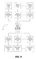
- any, or all, of the switches 300 , 400 , 500 , 600 , 700 , and 800 may be utilized to provide an improved optical communication system 900 as shown in FIG. 9 .
- the improved communication system 900 is substantially the same as the communication system 100 shown in FIG. 1 , except that the conventional optical switch 130 is replaced with one of the improved optical switches 300 , 400 , 500 , 600 , 700 , or 800 .
- the communication system 900 may further be provided with the improved optical switches in a variety of other locations where switching is required.
- the optical switches 300 , 400 , 500 , 600 , 700 , and 800 may replace any conventional optical switch or switches within existing optical systems.
- the optical switches 300 , 400 , 500 , 600 , 700 , and 800 help reduce beam divergence thereby allowing optical signals from input optical waveguides to be more efficiently coupled to their associated output optical waveguides. Furthermore, the reduced beam divergence of the improved optical switches reduces cross talk inside the optical switches. Consequently, switching loss is reduced.
- the optical switches 300 , 400 , 500 , 600 , 700 , and 800 may also be provided with smaller micro-mirrors, thus allowing for increased speed and reduced cost.
- FIG. 10 is a flow chart illustrating an embodiment of a method for optically switching an optical signal from one optical waveguide to another.
- a first optical waveguide, a second optical waveguide, and a refractive material are provided.
- the refractive material is provided with a refractive index greater than the refractive index of air.
- an optical signal is propagated from the first optical waveguide through the refractive material.
- the optical signal is reflected through the refractive material to the second optical waveguide.
- FIG. 11 is a flow chart illustrating another embodiment of an optical switching method.
- a first optical waveguide, a second optical waveguide, and an optical glass refractive material are provided.
- an anti-reflection coating is applied to the surface of the optical glass refractive material.
- an optical signal is propagated from the first optical waveguide through the optical glass refractive material.
- the optical signal is reflected through the refractive material to the second optical waveguide.
Landscapes
- Physics & Mathematics (AREA)
- General Physics & Mathematics (AREA)
- Optics & Photonics (AREA)
- Mechanical Light Control Or Optical Switches (AREA)
- Micromachines (AREA)
Priority Applications (2)
| Application Number | Priority Date | Filing Date | Title |
|---|---|---|---|
| US10/339,922 US6912335B2 (en) | 2003-01-10 | 2003-01-10 | Optical switch with reduced beam divergence |
| JP2003429212A JP2004220013A (ja) | 2003-01-10 | 2003-12-25 | ビーム発散を減少させた光スイッチ |
Applications Claiming Priority (1)
| Application Number | Priority Date | Filing Date | Title |
|---|---|---|---|
| US10/339,922 US6912335B2 (en) | 2003-01-10 | 2003-01-10 | Optical switch with reduced beam divergence |
Publications (2)
| Publication Number | Publication Date |
|---|---|
| US20040136644A1 US20040136644A1 (en) | 2004-07-15 |
| US6912335B2 true US6912335B2 (en) | 2005-06-28 |
Family
ID=32711197
Family Applications (1)
| Application Number | Title | Priority Date | Filing Date |
|---|---|---|---|
| US10/339,922 Expired - Lifetime US6912335B2 (en) | 2003-01-10 | 2003-01-10 | Optical switch with reduced beam divergence |
Country Status (2)
| Country | Link |
|---|---|
| US (1) | US6912335B2 (ja) |
| JP (1) | JP2004220013A (ja) |
Cited By (2)
| Publication number | Priority date | Publication date | Assignee | Title |
|---|---|---|---|---|
| US20060093272A1 (en) * | 2004-11-03 | 2006-05-04 | Fenwick David M | Optical connections and methods of forming optical connections |
| US20060093361A1 (en) * | 2004-11-03 | 2006-05-04 | Fenwick David M | Optical bus system |
Families Citing this family (5)
| Publication number | Priority date | Publication date | Assignee | Title |
|---|---|---|---|---|
| US6912335B2 (en) * | 2003-01-10 | 2005-06-28 | Agilent Technologies, Inc. | Optical switch with reduced beam divergence |
| US7231106B2 (en) * | 2005-09-30 | 2007-06-12 | Lucent Technologies Inc. | Apparatus for directing an optical signal from an input fiber to an output fiber within a high index host |
| CN108345068B (zh) * | 2017-01-25 | 2020-01-17 | 华为技术有限公司 | 光开关和光交换系统 |
| US10197971B1 (en) * | 2017-08-02 | 2019-02-05 | International Business Machines Corporation | Integrated optical circuit for holographic information processing |
| CN117134827A (zh) * | 2022-05-20 | 2023-11-28 | 华为技术有限公司 | 光通信设备 |
Citations (5)
| Publication number | Priority date | Publication date | Assignee | Title |
|---|---|---|---|---|
| EP0826995A1 (en) | 1996-08-28 | 1998-03-04 | Hewlett-Packard Company | An optoelectronic module having its components mounted on a single mounting member |
| EP1041707A2 (en) | 1999-03-30 | 2000-10-04 | Agilent Technologies Inc | Optical cross-connect switch using electrostatic surface actuators |
| US20020118907A1 (en) * | 2001-02-28 | 2002-08-29 | Akio Sugama | Optical wiring substrate, method of manufacturing optical wiring substrate and multilayer optical wiring |
| US6567206B1 (en) * | 2001-12-20 | 2003-05-20 | St. Clair Intellectual Property Consultants, Inc. | Multi-stage optical switching device |
| US20040136644A1 (en) * | 2003-01-10 | 2004-07-15 | Fouquet Julie E. | Optical switch with reduced beam divergence |
-
2003
- 2003-01-10 US US10/339,922 patent/US6912335B2/en not_active Expired - Lifetime
- 2003-12-25 JP JP2003429212A patent/JP2004220013A/ja not_active Withdrawn
Patent Citations (8)
| Publication number | Priority date | Publication date | Assignee | Title |
|---|---|---|---|---|
| EP0826995A1 (en) | 1996-08-28 | 1998-03-04 | Hewlett-Packard Company | An optoelectronic module having its components mounted on a single mounting member |
| US5848211A (en) | 1996-08-28 | 1998-12-08 | Hewlett-Packard Company | Photonics module having its components mounted on a single mounting member |
| EP1041707A2 (en) | 1999-03-30 | 2000-10-04 | Agilent Technologies Inc | Optical cross-connect switch using electrostatic surface actuators |
| US6215222B1 (en) | 1999-03-30 | 2001-04-10 | Agilent Technologies, Inc. | Optical cross-connect switch using electrostatic surface actuators |
| US20020118907A1 (en) * | 2001-02-28 | 2002-08-29 | Akio Sugama | Optical wiring substrate, method of manufacturing optical wiring substrate and multilayer optical wiring |
| US6810160B2 (en) * | 2001-02-28 | 2004-10-26 | Fujitsu Limited | Optical wiring substrate, method of manufacturing optical wiring substrate and multilayer optical wiring |
| US6567206B1 (en) * | 2001-12-20 | 2003-05-20 | St. Clair Intellectual Property Consultants, Inc. | Multi-stage optical switching device |
| US20040136644A1 (en) * | 2003-01-10 | 2004-07-15 | Fouquet Julie E. | Optical switch with reduced beam divergence |
Non-Patent Citations (1)
| Title |
|---|
| A. E. Siegmon, " Optical Resonators and Lens Waveguides," An Introduction to Lasers and Masers, Chapter 8, 1971, pp. 305-315. |
Cited By (6)
| Publication number | Priority date | Publication date | Assignee | Title |
|---|---|---|---|---|
| US20060093272A1 (en) * | 2004-11-03 | 2006-05-04 | Fenwick David M | Optical connections and methods of forming optical connections |
| US20060093361A1 (en) * | 2004-11-03 | 2006-05-04 | Fenwick David M | Optical bus system |
| US7400790B2 (en) | 2004-11-03 | 2008-07-15 | Hewlett-Packard Development Company, L.P. | Optical connections and methods of forming optical connections |
| US20090034910A1 (en) * | 2004-11-03 | 2009-02-05 | David Martin Fenwick | Optical Connections And Methods Of Forming Optical Connections |
| US7693362B2 (en) | 2004-11-03 | 2010-04-06 | Hewlett-Packard Development Company, L.P. | Optical connections and methods of forming optical connections |
| US8059927B2 (en) | 2004-11-03 | 2011-11-15 | Hewlett-Packard Development Company, L.P. | Optical connections and methods of forming optical connections |
Also Published As
| Publication number | Publication date |
|---|---|
| US20040136644A1 (en) | 2004-07-15 |
| JP2004220013A (ja) | 2004-08-05 |
Similar Documents
| Publication | Publication Date | Title |
|---|---|---|
| US5943454A (en) | Freespace optical bypass-exchange switch | |
| US6466711B1 (en) | Planar array optical switch and method | |
| US6539132B2 (en) | Acousto-optical switch for fiber optic lines | |
| US5757994A (en) | Three-part optical coupler | |
| US6618519B2 (en) | Switch and variable optical attenuator for single or arrayed optical channels | |
| US6718114B2 (en) | Variable optical attenuator of optical path conversion | |
| US6483961B1 (en) | Dual refraction index collimator for an optical switch | |
| US11199665B2 (en) | Optical device for redirecting optical signals | |
| US20070230868A1 (en) | Optical reflector, optical system and optical multiplexer/demultiplexer device | |
| US6912335B2 (en) | Optical switch with reduced beam divergence | |
| US6473544B1 (en) | Optical switch having equalized beam spreading in all connections | |
| US5930044A (en) | Deflecting element having a switchable liquid crystalline material | |
| US6867920B2 (en) | Optical beam-steering switching system having beam coupling control | |
| CN1929344B (zh) | 高动态范围集成接收器 | |
| US20050141805A1 (en) | Optical device and movable reflector | |
| US6678438B2 (en) | Apparatus and method for switching an optical path | |
| US6970615B1 (en) | Compact high-stability optical switches | |
| JPWO2004003652A1 (ja) | 反射型可変光偏向器及びそれを用いた光デバイス | |
| US6785439B2 (en) | Switching using three-dimensional rewriteable waveguide in photosensitive media | |
| JP6411899B2 (ja) | マルチコアファイバ接続装置およびシステム | |
| US20030048983A1 (en) | Fiber optic switching system | |
| JP4400317B2 (ja) | 光部品 | |
| WO2005116707A1 (en) | Improved variable optical attenuator | |
| JP4502064B2 (ja) | 光部品および可動反射装置 | |
| KR19990083119A (ko) | 광 스위치 |
Legal Events
| Date | Code | Title | Description |
|---|---|---|---|
| AS | Assignment |
Owner name: AGILENT TECHNOLOGIES, INC., COLORADO Free format text: ASSIGNMENT OF ASSIGNORS INTEREST;ASSIGNORS:FOUQUET, JULIE E.;HOKE, CHARLES D.;REEL/FRAME:013659/0010 Effective date: 20030108 |
|
| STCF | Information on status: patent grant |
Free format text: PATENTED CASE |
|
| AS | Assignment |
Owner name: AVAGO TECHNOLOGIES GENERAL IP PTE. LTD., SINGAPORE Free format text: ASSIGNMENT OF ASSIGNORS INTEREST;ASSIGNOR:AGILENT TECHNOLOGIES, INC.;REEL/FRAME:017207/0020 Effective date: 20051201 |
|
| AS | Assignment |
Owner name: AVAGO TECHNOLOGIES FIBER IP (SINGAPORE) PTE. LTD., Free format text: ASSIGNMENT OF ASSIGNORS INTEREST;ASSIGNOR:AVAGO TECHNOLOGIES GENERAL IP (SINGAPORE) PTE. LTD.;REEL/FRAME:017675/0199 Effective date: 20060127 |
|
| FPAY | Fee payment |
Year of fee payment: 4 |
|
| FPAY | Fee payment |
Year of fee payment: 8 |
|
| AS | Assignment |
Owner name: AVAGO TECHNOLOGIES GENERAL IP (SINGAPORE) PTE. LTD Free format text: MERGER;ASSIGNOR:AVAGO TECHNOLOGIES FIBER IP (SINGAPORE) PTE. LTD.;REEL/FRAME:030369/0672 Effective date: 20121030 |
|
| AS | Assignment |
Owner name: DEUTSCHE BANK AG NEW YORK BRANCH, AS COLLATERAL AGENT, NEW YORK Free format text: PATENT SECURITY AGREEMENT;ASSIGNOR:AVAGO TECHNOLOGIES GENERAL IP (SINGAPORE) PTE. LTD.;REEL/FRAME:032851/0001 Effective date: 20140506 Owner name: DEUTSCHE BANK AG NEW YORK BRANCH, AS COLLATERAL AG Free format text: PATENT SECURITY AGREEMENT;ASSIGNOR:AVAGO TECHNOLOGIES GENERAL IP (SINGAPORE) PTE. LTD.;REEL/FRAME:032851/0001 Effective date: 20140506 |
|
| AS | Assignment |
Owner name: AVAGO TECHNOLOGIES GENERAL IP (SINGAPORE) PTE. LTD., SINGAPORE Free format text: TERMINATION AND RELEASE OF SECURITY INTEREST IN PATENT RIGHTS (RELEASES RF 032851-0001);ASSIGNOR:DEUTSCHE BANK AG NEW YORK BRANCH, AS COLLATERAL AGENT;REEL/FRAME:037689/0001 Effective date: 20160201 Owner name: AVAGO TECHNOLOGIES GENERAL IP (SINGAPORE) PTE. LTD Free format text: TERMINATION AND RELEASE OF SECURITY INTEREST IN PATENT RIGHTS (RELEASES RF 032851-0001);ASSIGNOR:DEUTSCHE BANK AG NEW YORK BRANCH, AS COLLATERAL AGENT;REEL/FRAME:037689/0001 Effective date: 20160201 |
|
| AS | Assignment |
Owner name: BANK OF AMERICA, N.A., AS COLLATERAL AGENT, NORTH CAROLINA Free format text: PATENT SECURITY AGREEMENT;ASSIGNOR:AVAGO TECHNOLOGIES GENERAL IP (SINGAPORE) PTE. LTD.;REEL/FRAME:037808/0001 Effective date: 20160201 Owner name: BANK OF AMERICA, N.A., AS COLLATERAL AGENT, NORTH Free format text: PATENT SECURITY AGREEMENT;ASSIGNOR:AVAGO TECHNOLOGIES GENERAL IP (SINGAPORE) PTE. LTD.;REEL/FRAME:037808/0001 Effective date: 20160201 |
|
| AS | Assignment |
Owner name: AVAGO TECHNOLOGIES GENERAL IP (SINGAPORE) PTE. LTD Free format text: CORRECTIVE ASSIGNMENT TO CORRECT THE NAME OF THE ASSIGNEE PREVIOUSLY RECORDED ON REEL 017207 FRAME 0020. ASSIGNOR(S) HEREBY CONFIRMS THE ASSIGNMENT;ASSIGNOR:AGILENT TECHNOLOGIES, INC.;REEL/FRAME:038633/0001 Effective date: 20051201 |
|
| FPAY | Fee payment |
Year of fee payment: 12 |
|
| AS | Assignment |
Owner name: AVAGO TECHNOLOGIES GENERAL IP (SINGAPORE) PTE. LTD., SINGAPORE Free format text: TERMINATION AND RELEASE OF SECURITY INTEREST IN PATENTS;ASSIGNOR:BANK OF AMERICA, N.A., AS COLLATERAL AGENT;REEL/FRAME:041710/0001 Effective date: 20170119 Owner name: AVAGO TECHNOLOGIES GENERAL IP (SINGAPORE) PTE. LTD Free format text: TERMINATION AND RELEASE OF SECURITY INTEREST IN PATENTS;ASSIGNOR:BANK OF AMERICA, N.A., AS COLLATERAL AGENT;REEL/FRAME:041710/0001 Effective date: 20170119 |
|
| AS | Assignment |
Owner name: AVAGO TECHNOLOGIES INTERNATIONAL SALES PTE. LIMITE Free format text: MERGER;ASSIGNOR:AVAGO TECHNOLOGIES GENERAL IP (SINGAPORE) PTE. LTD.;REEL/FRAME:047196/0097 Effective date: 20180509 |
|
| AS | Assignment |
Owner name: AVAGO TECHNOLOGIES INTERNATIONAL SALES PTE. LIMITE Free format text: CORRECTIVE ASSIGNMENT TO CORRECT THE EXECUTION DATE PREVIOUSLY RECORDED AT REEL: 047196 FRAME: 0097. ASSIGNOR(S) HEREBY CONFIRMS THE MERGER;ASSIGNOR:AVAGO TECHNOLOGIES GENERAL IP (SINGAPORE) PTE. LTD.;REEL/FRAME:048555/0510 Effective date: 20180905 |
|
| AS | Assignment |
Owner name: BROADCOM INTERNATIONAL PTE. LTD., SINGAPORE Free format text: ASSIGNMENT OF ASSIGNORS INTEREST;ASSIGNOR:AVAGO TECHNOLOGIES INTERNATIONAL SALES PTE. LIMITED;REEL/FRAME:053771/0901 Effective date: 20200826 |
|
| AS | Assignment |
Owner name: AVAGO TECHNOLOGIES INTERNATIONAL SALES PTE. LIMITED, SINGAPORE Free format text: MERGER;ASSIGNORS:AVAGO TECHNOLOGIES INTERNATIONAL SALES PTE. LIMITED;BROADCOM INTERNATIONAL PTE. LTD.;REEL/FRAME:062952/0850 Effective date: 20230202 |