US6900928B2 - Method of patterning and fabricating poled dielectric microstructures within dielectric materials - Google Patents
Method of patterning and fabricating poled dielectric microstructures within dielectric materials Download PDFInfo
- Publication number
- US6900928B2 US6900928B2 US10/100,738 US10073802A US6900928B2 US 6900928 B2 US6900928 B2 US 6900928B2 US 10073802 A US10073802 A US 10073802A US 6900928 B2 US6900928 B2 US 6900928B2
- Authority
- US
- United States
- Prior art keywords
- dielectric
- poled
- dielectric material
- structures
- linbo
- Prior art date
- Legal status (The legal status is an assumption and is not a legal conclusion. Google has not performed a legal analysis and makes no representation as to the accuracy of the status listed.)
- Expired - Lifetime, expires
Links
- 238000000034 method Methods 0.000 title claims abstract description 174
- 239000003989 dielectric material Substances 0.000 title claims abstract description 162
- 238000000059 patterning Methods 0.000 title claims abstract description 47
- 238000004519 manufacturing process Methods 0.000 claims abstract description 40
- 229910003327 LiNbO3 Inorganic materials 0.000 claims description 85
- VYPSYNLAJGMNEJ-UHFFFAOYSA-N Silicium dioxide Chemical compound O=[Si]=O VYPSYNLAJGMNEJ-UHFFFAOYSA-N 0.000 claims description 68
- 230000003287 optical effect Effects 0.000 claims description 57
- 239000000463 material Substances 0.000 claims description 56
- 229910052681 coesite Inorganic materials 0.000 claims description 34
- 229910052906 cristobalite Inorganic materials 0.000 claims description 34
- 239000000377 silicon dioxide Substances 0.000 claims description 34
- 229910052682 stishovite Inorganic materials 0.000 claims description 34
- 229910052905 tridymite Inorganic materials 0.000 claims description 34
- 238000006243 chemical reaction Methods 0.000 claims description 30
- 239000013078 crystal Substances 0.000 claims description 26
- 239000002861 polymer material Substances 0.000 claims description 19
- 229910003334 KNbO3 Inorganic materials 0.000 claims description 17
- BPQQTUXANYXVAA-UHFFFAOYSA-N Orthosilicate Chemical compound [O-][Si]([O-])([O-])[O-] BPQQTUXANYXVAA-UHFFFAOYSA-N 0.000 claims description 17
- 239000000835 fiber Substances 0.000 claims description 17
- 239000005350 fused silica glass Substances 0.000 claims description 17
- YBMRDBCBODYGJE-UHFFFAOYSA-N germanium oxide Inorganic materials O=[Ge]=O YBMRDBCBODYGJE-UHFFFAOYSA-N 0.000 claims description 17
- 239000011521 glass Substances 0.000 claims description 11
- 238000012545 processing Methods 0.000 claims description 11
- 230000003321 amplification Effects 0.000 claims description 10
- 239000007788 liquid Substances 0.000 claims description 10
- 238000003199 nucleic acid amplification method Methods 0.000 claims description 10
- 230000010355 oscillation Effects 0.000 claims description 10
- 238000004891 communication Methods 0.000 claims description 9
- 238000001514 detection method Methods 0.000 claims description 9
- 239000006185 dispersion Substances 0.000 claims description 9
- 238000007648 laser printing Methods 0.000 claims description 9
- 239000013307 optical fiber Substances 0.000 claims description 9
- 239000005266 side chain polymer Substances 0.000 claims description 9
- IJGRMHOSHXDMSA-UHFFFAOYSA-N nitrogen Substances N#N IJGRMHOSHXDMSA-UHFFFAOYSA-N 0.000 claims description 6
- 229910052757 nitrogen Inorganic materials 0.000 claims description 4
- 238000010438 heat treatment Methods 0.000 claims description 2
- -1 KTiOPO4 Inorganic materials 0.000 claims 32
- 229910012463 LiTaO3 Inorganic materials 0.000 claims 24
- QJGQUHMNIGDVPM-UHFFFAOYSA-N nitrogen group Chemical group [N] QJGQUHMNIGDVPM-UHFFFAOYSA-N 0.000 claims 2
- 239000003795 chemical substances by application Substances 0.000 claims 1
- 230000005684 electric field Effects 0.000 description 41
- 230000015572 biosynthetic process Effects 0.000 description 9
- 238000010899 nucleation Methods 0.000 description 9
- 230000006911 nucleation Effects 0.000 description 8
- 239000007787 solid Substances 0.000 description 8
- 238000009826 distribution Methods 0.000 description 7
- 230000010287 polarization Effects 0.000 description 6
- 238000013461 design Methods 0.000 description 5
- WSMQKESQZFQMFW-UHFFFAOYSA-N 5-methyl-pyrazole-3-carboxylic acid Chemical compound CC1=CC(C(O)=O)=NN1 WSMQKESQZFQMFW-UHFFFAOYSA-N 0.000 description 4
- GQYHUHYESMUTHG-UHFFFAOYSA-N lithium niobate Chemical compound [Li+].[O-][Nb](=O)=O GQYHUHYESMUTHG-UHFFFAOYSA-N 0.000 description 4
- 238000009792 diffusion process Methods 0.000 description 3
- 150000002500 ions Chemical group 0.000 description 3
- 230000000737 periodic effect Effects 0.000 description 3
- 230000002269 spontaneous effect Effects 0.000 description 3
- 239000000758 substrate Substances 0.000 description 3
- 238000005457 optimization Methods 0.000 description 2
- 230000011218 segmentation Effects 0.000 description 2
- 239000004065 semiconductor Substances 0.000 description 2
- 238000013459 approach Methods 0.000 description 1
- 238000012512 characterization method Methods 0.000 description 1
- 230000009977 dual effect Effects 0.000 description 1
- 238000011835 investigation Methods 0.000 description 1
- 238000005342 ion exchange Methods 0.000 description 1
- 230000005855 radiation Effects 0.000 description 1
- 230000003362 replicative effect Effects 0.000 description 1
- 238000012216 screening Methods 0.000 description 1
Images


Classifications
-
- G—PHYSICS
- G02—OPTICS
- G02F—OPTICAL DEVICES OR ARRANGEMENTS FOR THE CONTROL OF LIGHT BY MODIFICATION OF THE OPTICAL PROPERTIES OF THE MEDIA OF THE ELEMENTS INVOLVED THEREIN; NON-LINEAR OPTICS; FREQUENCY-CHANGING OF LIGHT; OPTICAL LOGIC ELEMENTS; OPTICAL ANALOGUE/DIGITAL CONVERTERS
- G02F1/00—Devices or arrangements for the control of the intensity, colour, phase, polarisation or direction of light arriving from an independent light source, e.g. switching, gating or modulating; Non-linear optics
- G02F1/35—Non-linear optics
- G02F1/355—Non-linear optics characterised by the materials used
- G02F1/3558—Poled materials, e.g. with periodic poling; Fabrication of domain inverted structures, e.g. for quasi-phase-matching [QPM]
Definitions
- the present invention relates generally to the engineering of dielectric materials and more specifically to methods of patterning and fabricating poled dielectric microstructures within dielectric materials.
- Patterning and fabrication of microstructures within dielectric materials enable a new dimension in material engineering and thus opens up new opportunities for the use of dielectric materials in a variety of applications.
- the ability to design and process semiconductor materials for integrated circuits (IC) and semiconductor lasers is analogous to such a new dimension and opportunities now presented to dielectric materials.
- ferroelectric materials such as periodically poled lithium niobate (PPLN), periodically poled lithium tantalate (PPLT) and periodically poled KTiOPO 4 (PPKTP).
- PPLN periodically poled lithium niobate
- PPLT periodically poled lithium tantalate
- PPKTP periodically poled KTiOPO 4
- Example applications of poled dielectric microstructures are quasi-phase-matched (QPM) nonlinear frequency conversion in dielectric materials with second order nonlinear susceptibilities.
- QPM quasi-phase-matched
- UV and visible light can be generated via second harmonic generation (SHG) or sum frequency generation (SFG);
- infrared can be generated via difference frequency generation (DFG), optical parametric oscillation (OPO), optical parametric amplification (OPA) and optical parametric generation (OPG);
- OFM optical frequency mixers
- Further examples include electro-optic (EO) modulators for beam scanners, sensors, high-speed modulators, etc.
- One of the major factors for the realization of the above example applications depends upon the ability to patterning and fabrication of the desired microstructures within the proper materials.
- the prior art provides a basic patterning and fabrication approach such as ferroelectric domain reversals via electric field poling or thermal poling.
- the desired patterned structures require finer microstructures such as shorter ferroelectric domain period or pattern structures with aperiodic periods, the challenge in achieving the desired pattern structures arises.
- those methods can't necessarily be used or optimized for the fabrication of several other proper materials.
- those methods also might encounter the scalability and yield issues in the fabrication of large area patterned microstructures.
- U.S. Pat. No. 5,786,926 to Yamada describes an electro-optical device having inverted domains formed inside a ferroelectric substrate and electro-optical unit utilizing thereof.
- U.S. Pat. No. 5,652,674 to Mizuuchi et al. describes a method for manufacturing domain-inverted region, optical wavelength conversion device utilizing such domain-inverted region and method for fabricating such device.
- a poled dielectric microstructure within a dielectric material is provided.
- the poled dielectric microstructure is then segmented into a plurality of independent sub-structures.
- the poled dielectric microstructures are then fabricated within each of the plurality of independent sub-structures. Additional processes and a novel poling setup for improving and implementing this patterning and fabrication method are also disclosed.
- FIGS. 1A , 2 A, 3 A, 4 A and 5 A schematically illustrate prior art for patterning and fabrication of poled dielectric microstructures.
- FIG. 1B schematically illustrates a top view preferred embodiment of the present invention for patterning and fabricating poled dielectric microstructures.
- FIGS. 2B and 2C schematically illustrate a top view improvement to the preferred embodiment of the present invention.
- FIGS. 3B and 3C schematically illustrate a top view further improvement to the preferred embodiment of the present invention.
- FIGS. 4B and 4C schematically illustrate a side-view of the present invention for simultaneously patterning electrodes on both sides of a dielectric material.
- FIGS. 4D and 4E schematically illustrate an improvement to the side-view of the present invention for simultaneously patterning electrodes on both sides of a dielectric material of FIGS. 4B and 4C .
- FIGS. 5B and 5C schematically illustrate an improvement to the preferred embodiment of the present invention by implementing a confinement layer in dielectric materials.
- FIGS. 5D and 5E schematically illustrate a further improvement to the preferred embodiment of the present invention by the dual-side electrode patterning and by implementing a confined layer within the dielectric materials.
- FIG. 6 schematically illustrates a conventional liquid contact electrode setup with which the preferred embodiment of the present invention may be achieved.
- FIG. 7 schematically illustrates a novel setup with which the poling of the preferred embodiment of the present invention may be achieved.
- FIG. 8 schematically illustrates the implementation of present invention by the novel poling setup of FIG. 7 .
- ferroelectric materials have spontaneous polarization, i.e. they have internal dipole moments. Desired domain configurations (domains or domain patterns) within the ferroelectric may be formed by controlling the direction of these internal dipole moments.
- Desired domain configurations domains or domain patterns
- One of the more significant ways to form domain patterns is the application of an electric field to the material to change the direction of spontaneous polarization in desired regions, which is referred to as electric field poling.
- This invention discloses a novel patterning and fabrication method of poled dielectric microstructures wherein the desired microstructures within a body of dielectric materials can be fabricated by segmenting the patterning into several optimized structures. This allows fabrication of poled dielectric microstructures in each independent section and thus achieves fabrication optimization. High-quality, high-yield and scaleable poled dielectric microstructures can be patterned and fabricated through this method. Additional processes and poling setups for improving and implementing this patterning and fabrication method are also disclosed.
- a generic patterning and fabrication method is disclosed for poled dielectric microstructures or domains as the preferred embodiment of the present invention. Desired microstructures/domains within a body of dielectric materials are fabricated by segmenting the patterning into several optimized independent sections which permits fabrication of poled domains in each independent section and thus achieves fabrication optimization.
- the patterning and fabrication of poled dielectric microstructures/domains in this invention are illustrated by domain reversal within the ferroelectric materials.
- the described patterning and fabrication method can be applied to other non-ferroelectric dielectric materials such as glass materials or polymer materials.
- a dielectric material structure is provided and segmented into a plurality of independent sub-structures for patterning.
- the poled dielectric microstructures are then fabricated within each of the plurality of independent substructures.
- a poling station setup to achieve the optimized implementation of the proposed poling process.
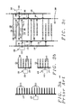
- FIG. 1A illustrates a prior art 8 cm of patterned dielectric material 10 having, for example a 4 micron period.
- Applying an electric field to electrodes 12 (connected to an electric source 17 via a conductive line 15 ) each having a width 14 and a quasi-phase matched (QPM) period 16 , induce individual domains 18 proximate the individual electrodes through the use of electric fields.
- QPM quasi-phase matched
- Undesirable electric field and electric dipole interference occurs within the body of dielectric material 10 during the poling process to form the domains 18 proximate electrodes 12 .
- the fabrication difficulties occur especially during the challenged short period poling (for example 4-micron period) or aperiodic period poling.
- FIG. 1B illustrates the preferred embodiment of the present invention.
- the large scale 4 cm patterned dielectric material 20 is decomposed into two sets of electrodes 22 , 24 and respective domains 26 , 28 (formed by applying an electric field to respective electrodes 22 , 24 ) each having a 8-micron poling period.
- Each respective set of electrodes 22 , 24 is connected to respective electrical sources 30 , 32 via respective conductive lines 23 , 25 .
- the poling process only occurs for a longer period poling (8-micron), which alleviates the electric field and electric dipole interference within the body 20 of dielectric material during the poling process.
- FIG. 2A schematically illustrates a prior art electrode scheme for a large scale patterned dielectric material having electrodes 40 connected to an electric source 42 via a conductive line 44 .
- the electrode scheme of the large scale patterned dielectric material is further divided into several subsets with smaller-area poling patterns. This will alleviate the scalability issues due to the large ratio between the total amount of poling time for large area structures ( FIG. 2A ) and the optimized poling time for each individual microstructures as shown in FIGS. 2B and 2C . This reduces the necessity to have good correlation of the uniform domain formation within different sections.
- FIG. 2B illustrates an electrode scheme wherein the prior art electrode scheme of FIG. 2A for a large scale patterned dielectric material has been subdivided into three subsets 58 , 68 , 78 having smaller-area poling patterns.
- Each respective subset 58 , 68 , 78 comprises respective electrodes 50 , 60 , 70 connected to a respective electric source 52 , 62 , 72 via respective conductive lines 54 , 64 , 74 .
- Respective domains 56 , 66 , 76 are induced proximate the individual electrodes 50 , 60 , 70 by applying an electric field to the respective electrodes 50 , 60 , 70 .
- FIG. 2C illustrates an electrode scheme wherein the prior art electrode scheme of FIG. 2A for a large scale patterned dielectric material 120 has been subdivided into four subsets 88 , 98 , 108 , 118 having smaller-area poling patterns.
- Each respective subset 88 , 98 , 108 , 118 comprises respective electrodes 80 , 90 , 100 , 110 connected to a respective electric source 82 , 92 , 102 , 112 via respective conductive lines 84 , 94 , 104 , 114 .
- respective domains 81 , 91 , 101 , 111 are induced in the dielectric material 120 proximate the respective electrodes 80 , 90 , 100 , 110 .
- FIGS. 3B and 3C Enhanced Nucleation Structures
- FIG. 3A schematically illustrates a prior art electrode scheme for a large scale patterned dielectric material similar to that shown in FIG. 2 A and having electrodes 121 connected to an electric source 122 via a conductive line 124 . Individual domains 123 are induced by the application of an electric field to electrodes 121 .
- the local electric field intensity is enhanced to thus enhance to formation of initial poling, that is nucleation.
- FIG. 3B illustrates an electrode scheme wherein the prior art electrode scheme of FIG. 3A for a large scale patterned dielectric material has been subdivided into two subsets 138 , 148 having smaller-area poling patterns.
- Each respective subset 138 , 148 comprises respective patterning electrodes 130 , 140 connected to a respective electric source 132 , 142 via respective conductive lines 134 , 144 .
- the patterning electrodes 130 , 140 each have respective nucleation electrode design 131 , 141 , which enhances the local electric field intensity and thus enhances to formation of initial poling.
- Respective nucleated domains 133 , 143 are induced proximate the individual nucleated electrode design electrodes 131 , 141 by applying an electric field to the respective electrodes 131 , 141 .
- FIG. 3C illustrates an electrode scheme wherein the prior art electrode scheme of FIG. 3A for a large scale patterned dielectric material 200 has been subdivided into four subsets 158 , 168 , 178 , 188 having smaller-area poling patterns.
- Each respective subset 158 , 168 , 178 , 188 comprises respective patterning electrodes 150 , 160 , 170 , 180 connected to a respective electric source 152 , 162 , 172 , 182 via respective conductive lines 154 , 164 , 174 , 184 .
- the patterning electrodes 150 , 160 , 170 , 180 each have respective nucleation electrodes 151 , 161 , 171 , 181 , which enhances the local electric field intensity and thus enhances formation of initial poling.
- Respective nucleated domains 156 , 166 , 176 , 186 are induced proximate the individual nucleated electrodes 150 , 160 , 170 , 180 by applying an electric field to the respective nucleated electrodes 151 , 161 , 171 , 181 .
- the above patterning and fabrication method of the preferred embodiment and the subset division improvement shown in FIGS. 2B and 2C and the nucleation improvement shown in FIGS. 3B and 3C can also be applied to simultaneous electrode patterning on both sides of the dielectric material to further enhance the poling quality.
- FIG. 4A illustrates a prior art patterning and fabrication of poled dielectric microstructure within dielectric material 300 which has a strong electric field and electric dipole interference 310 causing non-uniformity and non-symmetric quality on both sides of the patterned dielectric material 300 —Solid arrows 301 represent electric field distribution while dash arrows 302 represent dipole of ferroelectric domains.
- FIGS. 4B and 4C illustrate employing the method of the present invention on a patterned dielectric material 400 which reduces the field interference with improved uniformity.
- Microstructures are fabricated sequentially (as illustrated in FIGS. 4B and 4C ) according to the pattern segmentation.
- Solid arrows 401 represent electric field distribution while dash arrows 402 represent dipole of ferroelectric domains.
- FIGS. 4D and 4E illustrate a further improved method of FIGS. 4B , 4 C of the present invention on a patterned dielectric material 410 by simultaneously patterning electrodes on both sides of the dielectric material 410 , which results in very small interference and produces uniform quality on both sides of the patterned dielectric material 410 .
- Microstructures are fabricated sequentially (as illustrated in FIGS. 4D and 4E ) according to the pattern segmentation.
- Solid arrows 411 represent electric field distribution while dash arrows 412 represent dipole of ferroelectric domains.
- the above patterning and fabrication method of the preferred embodiment and the subset division improvement shown in FIGS. 2B and 2C , the nucleation improvement shown in FIGS. 3B and 3C , and the symmetry improvement shown in FIGS. 4D and 4E can also be improved by implementing a confined layer within dielectric materials.
- the function of a confined layer is to alter the material properties and thus suppress the formation of poling within the confinement region.
- Example of confinement layer within dielectric materials can be formed by ion exchanged or ion-diffusion to dielectric materials. It has been well known that the ion-exchanged process can alter the material properties and thus will possibly suppress the formation of poling.
- Poled dielectric microstructures can thus be improved by engineering the ion-exchanged patterning in dielectric material, which suppress the domain formation according to the microstructure design.
- FIG. 5A illustrates a prior art fabricating of poled dielectric microstructures in ion-exchanged dielectric materials 500 .
- Solid arrows 501 represent electric field distribution while dash arrows 502 represent dipole of ferroelectric domains.
- FIGS. 5B and 5C illustrate an improvement method of the present invention to the fabrication of poled dielectric microstructure within a dielectric material 510 with an ion-exchanged pattern as a domain growth confinement layer.
- Solid arrows 511 represent electric field distribution while dash arrows 512 represent dipole of ferroelectric domains.
- FIGS. 5D and 5E illustrates a further improved method of the present invention to the fabrication of poled dielectric microstructure within a dielectric material 520 by simultaneously patterning electrodes on both sides of the dielectric materials with a confinement layer.
- Solid arrows 521 represent electric field distribution while dash arrows 522 represent dipole of ferroelectric domains
- such confinement layers within dielectric materials 510 , 520 can be formed by ion exchanged or ion-diffusion to dielectric materials 510 , 520 .
- the above-described patterning and fabrication method of the present invention can also be applied to different crystal orientation, that is X-cut, Y-cut or Z-cut.
- Example ferroelectric materials include lithium niobate (LiNbO 3 ), lithium tantalate (LiTaO 3 ), KTiOPO 4 (KTP), KNbO 3 (KDP), BaB 2 O 4 (BBO) and their family such as MgO:LiNbO 3 , ZnO:LiNbO 3 etc. and material with pre-ion (proton or Ti) diffusion before poling.
- the LiTaO 3 and their family also include crystals at different formats.
- More preferred ferroelectric materials include LiNbO 3 and LiTaO 3 and their family such as congruent LiNbO 3 (CLN) and stoichiometric LiNbO 3 (SLN); and the above crystals with doping such as MgO:CLN, ZnO:CLN, MgO:SLN, ZnO:SLN.
- CLN congruent LiNbO 3
- SSN stoichiometric LiNbO 3
- dielectric materials include: glass materials such as SiO 2 , GeO 2 SiO 2 , fused silica or silicate fiber; and polymer materials such as Dispersion Red 1 Side Chain polymer.
- FIG. 6 schematically illustrates a conventional prior art liquid contact electrode 702 poling setup 700 which may be used in accordance the practice of the present invention to electrically field pole dielectric material 712 .
- the conventional poling setup 700 of FIG. 6 utilizes liquid contact electrodes 702 connected to a high voltage supply 704 in a circuit having a current monitor 706 , a voltage monitor 708 and a resistor 710 .
- FIG. 7 schematically illustrates a novel poling setup 600 to electrically pole a dielectric material wafer 612 in accordance the practice of the present invention, which permits independent poling of each section.
- the poling setup 600 includes dielectric material wafer 612 supported by wafer base 614 and having electrodes electrically connected to voltage and current supply 618 via conductive lines 616 within vacuum chamber 620 .
- the vacuum within chamber 620 is achieved using a vacuum pump 630 and dry nitrogen may be introduced into chamber 620 from a dry nitrogen source 632 .
- the voltage and current supply 618 is connected through switching box 622 to a high voltage facility 624 .
- a computer 626 controls the electric field poling process in accordance with the method of the present invention as well as the position of wafer 612 using a position controller 628 .
- the voltage can preferably be applied sequentially through the pre-wired conductive lines 616 with external switching control via switching box 622 /computer 626 , or more preferably through moving stages to each individual sub-section contact points.
- the novel poling setup 600 of FIG. 7 may also be equipped with a wafer 612 heating element 634 to adjust crystal properties of the dielectric material wafer 612 as it is well known that the material properties such as conductivity and coercive field can be changed through temperature variation of the wafer 612 .
- Patterned electrodes for fabricating dielectric material are decomposed into several subsets of electrodes. Each subset has a longer poling period and a smaller poling area as compared to the complete poled dielectric microstructures.
- Improved methods as described in this invention such as enhanced nucleation electrode design, dual side electrode patterning, and additional ion exchange in dielectric materials, can be incorporated into the patterning and fabrication processes.
- Each respective set of electrodes is connected to respective electrical sources via sub-section contact points. Poling of each section is performed via connecting each conductive sub-section contact point to a high voltage facility.
- the voltage can preferably be applied sequentially through the pre-wired conductive lines 616 to sub-section contact points with external switching control via switching box 622 /computer 626 , or more preferably through moving stages to each individual sub-section contact points.
- FIG. 8 schematically illustrates the implementation of present invention by the novel poling setup of FIG. 7 .
- Electrical field for poling 950 is applied to each individual section 900 , 910 , 920 , 930 sequentially.
- Adjacent sections, e.g. 900 , 910 ; 920 , 930 can be applied with an additional (optional) electric field 940 , which serves as a screening field to change the net electric filed distribution within the dielectric material 960 .
- the applications of the poled dielectric microstructures/domains patterned and fabricated in accordance with the present invention include:
- QPM quasi-phase matching
- conversion process can be through second harmonic generation (SHG), sum frequency generation (SFG), difference frequency generation (DFG), optical parametric oscillation (OPO), optical parametric amplification (OPA), optical parametric generation (OPG), cascaded frequency conversion, etc.;
- the fields of application can include a light source for laser displays, laser scanners, laser printing, laser spectroscopes, sensing and detection applications and, biology and medical applications;
- electro-optic (EO)-optic modulators for beam scanners, sensors and high-speed modulators, etc.
- AO acoustic-optical
Landscapes
- Physics & Mathematics (AREA)
- Nonlinear Science (AREA)
- General Physics & Mathematics (AREA)
- Optics & Photonics (AREA)
- Optical Modulation, Optical Deflection, Nonlinear Optics, Optical Demodulation, Optical Logic Elements (AREA)
Abstract
A method of patterning and fabricating poled dielectric microstructures in dielectric materials comprising the following steps. A poled dielectric microstructure within a dielectric material is provided. The poled dielectric microstructure is then segmented into a plurality of independent sub-structures. The poled dielectric microstructures are then fabricated within each of the plurality of independent sub-structures. Additional processes and a novel poling setup for improving and implementing this patterning and fabrication method are also disclosed.
Description
The present invention relates generally to the engineering of dielectric materials and more specifically to methods of patterning and fabricating poled dielectric microstructures within dielectric materials.
Patterning and fabrication of microstructures within dielectric materials enable a new dimension in material engineering and thus opens up new opportunities for the use of dielectric materials in a variety of applications. The ability to design and process semiconductor materials for integrated circuits (IC) and semiconductor lasers is analogous to such a new dimension and opportunities now presented to dielectric materials.
The feasibility to perform microstructure engineering within dielectric materials has been shown in, for example, domain reversals of ferroelectric materials such as periodically poled lithium niobate (PPLN), periodically poled lithium tantalate (PPLT) and periodically poled KTiOPO4 (PPKTP). Progress has also been shown in other materials such as poling in glass materials or poling in polymer materials.
Example applications of poled dielectric microstructures are quasi-phase-matched (QPM) nonlinear frequency conversion in dielectric materials with second order nonlinear susceptibilities. For example: (1) UV and visible light can be generated via second harmonic generation (SHG) or sum frequency generation (SFG); (2) infrared can be generated via difference frequency generation (DFG), optical parametric oscillation (OPO), optical parametric amplification (OPA) and optical parametric generation (OPG); and (3) optical frequency mixers (OFM) can be used for telecommunication and optical signal processing. Further examples include electro-optic (EO) modulators for beam scanners, sensors, high-speed modulators, etc.
One of the major factors for the realization of the above example applications depends upon the ability to patterning and fabrication of the desired microstructures within the proper materials. The prior art provides a basic patterning and fabrication approach such as ferroelectric domain reversals via electric field poling or thermal poling. However, as the desired patterned structures require finer microstructures such as shorter ferroelectric domain period or pattern structures with aperiodic periods, the challenge in achieving the desired pattern structures arises. Moreover, those methods can't necessarily be used or optimized for the fabrication of several other proper materials. In addition, those methods also might encounter the scalability and yield issues in the fabrication of large area patterned microstructures.
One of the key challenges in the poling of dielectric microstructures is the electric field and electric dipole interference within the body of dielectric materials during the electric field poling process. Such electric field and electric dipole interference results in non-uniform domain structures and difficulties in generating domain with short pitch (period). Additional challenges in poling of dielectric microstructures come from the scalability of the poling area. As the poling area increases, the total required poling time will also increase. The large ratio between the total amount of poling time for large area structures and the optimized poling time for each individual microstructure enhances the fabrication difficulty for generating large area and uniform microstructures.
Other challenges in the poling of dielectric microstructures include the generation of uniform high nucleation density (as seeding in the poling process) under high electric fields and the formation of uniform microstructures under optimized electric fields.
The article “Domain kinetics in the formation of a periodic domain structure in lithium niobate,” V. Y. Shur et al., Physics of the Solid State, Vol. 41, No. 10, pages 1681-1687, October 1999, describes the experimental investigation of the evolution of the domain structure in LiNbO3 with polarization switching in an electric field.
The article “Tunable ultraviolet radiation by second-harmonic generation in periodically poled lithium tantalate,” J. P. Meyn et al., Optics Letters, Vol. 22, No. 16, pages 1214-1216, Aug. 15, 1997, describes electric-field poling of fine-pitch ferroelectric domain gratings in lithium tantalate and characterization of nonlinear-optical properties by single-pass quasi-phase-matched second-harmonic generation (QPM SHG).
The article “Backswitch poling in lithium niobate for high-fidelity domain patterning and efficient blue light generation,” R. G. Batchko et al., Applied Physics Letters, Vol. 75, No. 12, pages 1673-1675, Sep. 20, 1999, describes an electric-field poling technique which incorporates spontaneous backswitching.
The article “Domain in ferroelectric MgO:LiNbO3 by applying electric fields,” A. Kuroda et al., Appl. Physics Lett., 69, pages 1565-1567, Sep. 9, 1996, describes inversion of an antiparallel ferroelectric domain in LiNbO3 doped with 5 mol % MgO (MgO:LN) at room temperature by application of a step-like electric field.
The article “Bulk Periodically Poled MgO-doped LiNbO3 by External Electric Field Application,” M. Nakamura et al., Jpn. J. Appl. Phys., Vol. 38, pages L512-L514, May 1, 1999, describes fabrication of bulk periodically poled MgO-doped LiNbO3 (PPMgLN) crystals by an electric field poling process using a liquid electrode technique.
The article “Bulk periodically poled MgO-LiNbO3 by corona discharge method,” A. Harada et al., Appl. Phys. Lett., 69 (18), pages 2629-2631, Oct. 28, 1996, describes a corona discharge method of the fabrication of bulk periodically poled MgO-LiNbO3 substrates.
The article “Second harmonic generation in electric poled X-cut MgO-doped LiNbO3 waveguides,” S. Sonoda et al., Appl. Phys. Lett., 70 (23), pages 3078-3080, Jun. 9, 1997, demonstrates that quasi-phase-matched second harmonic generation occurs in annealed proton-exchanged (APE) X-cut MgO 5 mol % doped LiNbO3 (MgO:LN) waveguides supporting a TE-mode guided wave.
U.S. Pat. No. 6,156,255 to Byer et al. describes electric field domain patterning.
U.S. Pat. No. 5,193,023 to Yamada et al. describes a method of controlling the domain of a nonlinear ferroelectric optics substrate.
U.S. Pat. No. 5,519,802 to Field et al. describes a method for making devices having a pattern poled structure and pattern poled structure devices.
U.S. Pat. No. 5,991,065 to Nutt et al. describes an addressable electro-optical modulator with periodically poled domain regions.
U.S. Pat. No. 5,986,798 to Karlsson et al. describes a method and arrangement for poling of optical crystals.
U.S. Pat. No. 5,875,053 to Webjorn et al. describes periodic electric field poled crystal waveguides.
U.S. Pat. No. 5,838,702 to Byer et al. describes a method of electrically controlling regions of ferroelectric polarization domains in solid state bodies.
U.S. Pat. No. 5,786,926 to Yamada describes an electro-optical device having inverted domains formed inside a ferroelectric substrate and electro-optical unit utilizing thereof.
U.S. Pat. No. 5,756,263 to Gupta et al. describes a method of inverting ferroelectric domains by application of controlled electric field.
U.S. Pat. No. 5,654,229 to Leplingard et al. describes a method for replicating periodic nonlinear coefficient patterning during and after growth of epitaxial ferroelectric oxide films.
U.S. Pat. No. 5,652,674 to Mizuuchi et al. describes a method for manufacturing domain-inverted region, optical wavelength conversion device utilizing such domain-inverted region and method for fabricating such device.
U.S. Pat. No. 5,615,041 to Field et al. describes fabrication of patterned poled dielectric structures and devices.
U.S. Pat. No. 6,002,515 to Mizuuchi et al. describes a method for producing polarization inversion part, optical wavelength conversion element using the same, and optical waveguide.
U.S. Pat. No. 5,744,073 to Nihei et al. describes fabrication of ferroelectric domain reversals.
U.S. Pat. No. 5,668,578 to Nihei et al. describes a method for fabricating ferroelectric domain reversals, and optical wavelength converter element.
U.S. Pat. No. 5,594,746 to Harada describes a method and apparatus for fabricating ferroelectric domain reversals.
U.S. Pat. No. 5,526,173 to Yamaguchi et al. describes a method of local domain control on nonlinear optical materials.
U.S. Pat. No. 5,249,250 to Yamada et al. describes an optical device having domain structure and method for manufacturing the same.
U.S. Pat. No. 5,748,361 to Gupta et al. describes a ferroelectric crystal having inverted domain structure.
U.S. Pat. No. 5,734,772 to Gopalan et al. describes an inverted domain structure in ferroelectric crystals with polarization in the crystal plane.
Accordingly, it is an object of one or more embodiments of the present invention to provide an improved method of patterning and fabricating poled dielectric microstructures within dielectric materials.
Other objects will appear hereinafter.
It has now been discovered that the above and other objects of the present invention may be accomplished in the following manner. Specifically, a poled dielectric microstructure within a dielectric material is provided. The poled dielectric microstructure is then segmented into a plurality of independent sub-structures. The poled dielectric microstructures are then fabricated within each of the plurality of independent sub-structures. Additional processes and a novel poling setup for improving and implementing this patterning and fabrication method are also disclosed.
The present invention will be more clearly understood from the following description taken in conjunction with the accompanying drawings in which like reference numerals designate similar or corresponding elements, regions and portions and in which:
By definition, ferroelectric materials have spontaneous polarization, i.e. they have internal dipole moments. Desired domain configurations (domains or domain patterns) within the ferroelectric may be formed by controlling the direction of these internal dipole moments. One of the more significant ways to form domain patterns is the application of an electric field to the material to change the direction of spontaneous polarization in desired regions, which is referred to as electric field poling.
This invention discloses a novel patterning and fabrication method of poled dielectric microstructures wherein the desired microstructures within a body of dielectric materials can be fabricated by segmenting the patterning into several optimized structures. This allows fabrication of poled dielectric microstructures in each independent section and thus achieves fabrication optimization. High-quality, high-yield and scaleable poled dielectric microstructures can be patterned and fabricated through this method. Additional processes and poling setups for improving and implementing this patterning and fabrication method are also disclosed.
A generic patterning and fabrication method is disclosed for poled dielectric microstructures or domains as the preferred embodiment of the present invention. Desired microstructures/domains within a body of dielectric materials are fabricated by segmenting the patterning into several optimized independent sections which permits fabrication of poled domains in each independent section and thus achieves fabrication optimization. The patterning and fabrication of poled dielectric microstructures/domains in this invention are illustrated by domain reversal within the ferroelectric materials. However, the described patterning and fabrication method can be applied to other non-ferroelectric dielectric materials such as glass materials or polymer materials.
Simply put, a dielectric material structure is provided and segmented into a plurality of independent sub-structures for patterning. The poled dielectric microstructures are then fabricated within each of the plurality of independent substructures. A poling station setup to achieve the optimized implementation of the proposed poling process.
Preferred Embodiment of the Present Invention
Undesirable electric field and electric dipole interference occurs within the body of dielectric material 10 during the poling process to form the domains 18 proximate electrodes 12. The fabrication difficulties occur especially during the challenged short period poling (for example 4-micron period) or aperiodic period poling.
Each respective set of electrodes 22, 24 is connected to respective electrical sources 30, 32 via respective conductive lines 23, 25. Thus, the poling process only occurs for a longer period poling (8-micron), which alleviates the electric field and electric dipole interference within the body 20 of dielectric material during the poling process.
Smaller-Area Poling Patterns—FIGS. 2B and 2C
As shown in FIGS. 2B and 2C , to further improve upon the preferred embodiment of present invention, the electrode scheme of the large scale patterned dielectric material is further divided into several subsets with smaller-area poling patterns. This will alleviate the scalability issues due to the large ratio between the total amount of poling time for large area structures (FIG. 2A ) and the optimized poling time for each individual microstructures as shown in FIGS. 2B and 2C . This reduces the necessity to have good correlation of the uniform domain formation within different sections.
Enhanced Nucleation Structures—FIGS. 3B and 3C
As shown in FIGS. 3B and 3C , to further enhance the uniformity of each small subset having a longer period (FIG. 1B ) and/or a smaller poling area (FIGS. 2B and 2C), the local electric field intensity is enhanced to thus enhance to formation of initial poling, that is nucleation.
Application of the Present Invention to Simultaneous Electrode Patterning on Both Sides of a Dielectric Material—FIGS. 4B to 4E
As shown in FIGS. 4B , 4C and FIGS. 4D , 4E, the above patterning and fabrication method of the preferred embodiment and the subset division improvement shown in FIGS. 2B and 2C and the nucleation improvement shown in FIGS. 3B and 3C can also be applied to simultaneous electrode patterning on both sides of the dielectric material to further enhance the poling quality.
Wherein FIGS. 4B and 4C illustrate employing the method of the present invention on a patterned dielectric material 400 which reduces the field interference with improved uniformity. Microstructures are fabricated sequentially (as illustrated in FIGS. 4B and 4C ) according to the pattern segmentation. Solid arrows 401 represent electric field distribution while dash arrows 402 represent dipole of ferroelectric domains.
Further Improvement of this Invention by Implementing A Confined Layer within Dielectric Materials FIGS. 5B to 5E.
The above patterning and fabrication method of the preferred embodiment and the subset division improvement shown in FIGS. 2B and 2C , the nucleation improvement shown in FIGS. 3B and 3C , and the symmetry improvement shown in FIGS. 4D and 4E , can also be improved by implementing a confined layer within dielectric materials. The function of a confined layer is to alter the material properties and thus suppress the formation of poling within the confinement region. Example of confinement layer within dielectric materials can be formed by ion exchanged or ion-diffusion to dielectric materials. It has been well known that the ion-exchanged process can alter the material properties and thus will possibly suppress the formation of poling. Poled dielectric microstructures can thus be improved by engineering the ion-exchanged patterning in dielectric material, which suppress the domain formation according to the microstructure design.
Wherein FIGS. 5B and 5C illustrate an improvement method of the present invention to the fabrication of poled dielectric microstructure within a dielectric material 510 with an ion-exchanged pattern as a domain growth confinement layer. Solid arrows 511 represent electric field distribution while dash arrows 512 represent dipole of ferroelectric domains.
As an example, such confinement layers within dielectric materials 510, 520 can be formed by ion exchanged or ion-diffusion to dielectric materials 510, 520.
The above-described patterning and fabrication method of the present invention can also be applied to different crystal orientation, that is X-cut, Y-cut or Z-cut.
The above-described patterning and fabrication method of the present invention can also be applied to various dielectric materials. Example ferroelectric materials include lithium niobate (LiNbO3), lithium tantalate (LiTaO3), KTiOPO4 (KTP), KNbO3 (KDP), BaB2O4 (BBO) and their family such as MgO:LiNbO3, ZnO:LiNbO3 etc. and material with pre-ion (proton or Ti) diffusion before poling. The LiTaO3 and their family also include crystals at different formats. More preferred ferroelectric materials include LiNbO3 and LiTaO3 and their family such as congruent LiNbO3 (CLN) and stoichiometric LiNbO3 (SLN); and the above crystals with doping such as MgO:CLN, ZnO:CLN, MgO:SLN, ZnO:SLN.
Other dielectric materials include: glass materials such as SiO2, GeO2SiO2, fused silica or silicate fiber; and polymer materials such as Dispersion Red 1 Side Chain polymer.
Poling Setups
The voltage and current supply 618 is connected through switching box 622 to a high voltage facility 624. A computer 626 controls the electric field poling process in accordance with the method of the present invention as well as the position of wafer 612 using a position controller 628.
The voltage can preferably be applied sequentially through the pre-wired conductive lines 616 with external switching control via switching box 622/computer 626, or more preferably through moving stages to each individual sub-section contact points.
The novel poling setup 600 of FIG. 7 may also be equipped with a wafer 612 heating element 634 to adjust crystal properties of the dielectric material wafer 612 as it is well known that the material properties such as conductivity and coercive field can be changed through temperature variation of the wafer 612.
Example of Using the Method of the Present Invention With the Novel Poling Setup
Patterned electrodes for fabricating dielectric material are decomposed into several subsets of electrodes. Each subset has a longer poling period and a smaller poling area as compared to the complete poled dielectric microstructures.
Improved methods as described in this invention, such as enhanced nucleation electrode design, dual side electrode patterning, and additional ion exchange in dielectric materials, can be incorporated into the patterning and fabrication processes.
Each respective set of electrodes is connected to respective electrical sources via sub-section contact points. Poling of each section is performed via connecting each conductive sub-section contact point to a high voltage facility. The voltage can preferably be applied sequentially through the pre-wired conductive lines 616 to sub-section contact points with external switching control via switching box 622/computer 626, or more preferably through moving stages to each individual sub-section contact points.
Applications of the Poled Dielectric Microstructures/Domains Patterned and Fabricated in Accordance with the Present Invention
The applications of the poled dielectric microstructures/domains patterned and fabricated in accordance with the present invention include:
1) quasi-phase matching (QPM) for nonlinear frequency conversion and generation of UV, visible light, infrared (IR), Q-switched and ultrashort pulses;
2) conversion process can be through second harmonic generation (SHG), sum frequency generation (SFG), difference frequency generation (DFG), optical parametric oscillation (OPO), optical parametric amplification (OPA), optical parametric generation (OPG), cascaded frequency conversion, etc.;
3) the fields of application can include a light source for laser displays, laser scanners, laser printing, laser spectroscopes, sensing and detection applications and, biology and medical applications;
4) optical frequency mixers for optical fiber communication and optical signal processing;
5) electro-optic (EO)-optic modulators for beam scanners, sensors and high-speed modulators, etc.; and
6) acoustic-optical (AO) modulators and grating assisted devices.
While particular embodiments of the present invention have been illustrated and described, it is not intended to limit the invention, except as defined by the following claims.
Claims (149)
1. A method of patterning and fabricating poled dielectric microstructures in a dielectric material, comprising the steps of:
providing a unitary poled dielectric microstructure within a dielectric material;
segmenting the unitary poled dielectric microstructure into a plurality of independent sub-structures; and
fabricating the poled dielectric microstructures within each of the plurality of independent sub-structures; wherein the patterned and fabricated poled dielectric microstructures are enhanced nucleated.
2. The method of claim 1 , wherein the dielectric material is comprised of ferroelectric materials, glass materials or polymer materials.
3. The method of claim 1 , wherein the dieledric material is comprised of LiNbO3, LiTaO3, KTiOPO4, KNbO3, BaB2O4, MgO:LiNbO3, ZnO:LiNbO3, SiO2, GeO2SiO2, fused silica, silicate fiber or Dispersion Red 1 Side Chain polymer.
4. The method of claim 1 , wherein the dielectric material is comprised of LiNbO3, LiTaO3,congruent LiNbO3(CLN), stoichiometric LiNbO3(SLN), MgO:CLN, ZnO:CLN, MgO:SLN or ZnO:SLN.
5. The method of claim 1 wherein the plurality of independent sub-structures have larger periods than the unitary poled dielectric microstructure.
6. The method of claim 1 , wherein the plurality of independent sub-structures have smaller-area poling patterns than the unitary poled dielectric microstructure.
7. The method of claim 1 , wherein the plurality of independent sub-structures have larger periods and smaller-area poling patterns than the unitary poled dielectric microstructure.
8. The method of claim 1 , wherein the poled dielectric microstructures are formed on both sides of the dielectric material.
9. The method of claim 1 , wherein the dielectric material has a crystal orientation that is X-cut, Y-cut or Z-cut.
10. The method of claim 1 , wherein the poled dielectric microstructures may be fabricated using liquid contact electrodes.
11. The method of claim 1 , wherein the poled dielectric microstructures may be fabricated by sequentially applying voltage through pre-wired conductive lines.
12. The method of claim 1 , wherein the poled dielectric microstructures may be fabricated by applying voltage through moving stages to contact points for each independent sub-structure.
13. The method of claim 1 , wherein the dielectric material has crystal properties that are adjusted through temperature variations of the dielectric material during fabrication of the poled dielectric microstructures.
14. The method of claim 1 , wherein the fabricated poled dielectric microstructures may be utilized in a:
1) quasi-phase matching (QPM) for nonlinear frequency conversion or generation of UV, visible light, infrared (IR), Q-switched pulses or ultrashort pulses;
2) conversion processes through second harmonic generation (SHG), sum frequency generation (SFG), difference frequency generation (DFG), optical parametric oscillation (OPO), optical parametric amplification (OPA), optical parametric generation (OPG) or cascaded frequency conversion;
3) a light source for laser displays, laser scanners, laser printing, laser spectroscopes, sensing or detection applications or biology or medical applications;
4) optical frequency mixers for optical fiber communication or optical signal processing,
5) electro-optic (EO) modulators for beam scanners, sensors or high-speed modulators; or
6) acoustic-optical (AO) modulators or grating assisted devices manner.
15. The method of claim 1 ; wherein the dielectric material includes at least one confinement layer; the at least one confinement layer including an ion-exchanged pattern as a domain growth confinement layer.
16. The method of claim 1 , wherein the dielectric material is comprised of ferroelectric materials or polymer materials.
17. The method of claim 1 , wherein the dielectric material is comprised of ferroelectric materials.
18. The method of claim 1 , wherein the dieledric material is comprised of LiNbO3, LiTaO3, KTiOPO4, KNbO3, BaB2O4, MgO:LiNbO3, ZnO:LiNbO3, SiO2, GeO2SiO2, fused silica or silicate fiber.
19. A method of patterning and fabricating poled dielectric microstructures in dielectric materials, comprising the steps of:
providing a unitary poled dieledric microstructure within a dielectric material; wherein the dielectric material is comprised of ferroelectric materials, glass materials or polymer materials;
segmenting the unitary poled dielectric microstructure into a plurality of independent sub-structures; and
fabricating the poled dielectric microstructures within each of the plurality of independent sub-structures; wherein the patterned and fabricated poled dielectric microstructures are enhanced nucleated.
20. The method of claim 19 , wherein the dielectric material is comprised of LiNbO3, LiTaO3, KTiOPO4, KNbO3, BaB2O4, MgO:LiNbO3, ZnO:LiNbO3, SiO2, GeO2SiO2, fused silica, silicate fiber or Dispersion Red 1 Side Chain polymer.
21. The method of claim 19 , wherein the dielectric material is comprised of a LiNbO3, LiTaO3, congruent LiNbO3, (CLN), stoichiometric LiNbO3(SLN), MgO:CLN, ZnO:CLN, MgO:SLN or ZnO:SLN.
22. The method of claim 19 , wherein the plurality of independent sub-structures have larger periods than the unitary poled dielectric microstructure.
23. The method of claim 19 , wherein the plurality of independent sub-structures have smaller-area poling patterns than the unitary poled dielectric microstructure.
24. The method of claim 19 , wherein the plurality of independent sub-structures have larger periods and smaller-area poling patterns than the unitary poled dielectric microstructure.
25. The method of claim 19 , wherein the poled dielectric microstructures are formed on both sides of the dielectric material.
26. The method of claim 19 , wherein the dielectric material has a crystal orientation that is X-cut, Y-cut or Z-cut.
27. The method of claim 19 , wherein the poled dielectric microstructures may be fabricated using liquid contact electrodes.
28. The method of claim 19 , wherein the poled dielectric microstructures may be fabricated by sequentially applying voltage through pre-wired conductive lines.
29. The method of claim 19 , wherein the poled dielectric microstructures may be fabricated by applying voltage through moving stages to contact points for each independent sub-structure.
30. The method of claim 19 , wherein the dielectric material has crystal properties that are adjusted through temperature variations of the dielectric material during fabrication of the poled dielectric microstructures.
31. The method of claim 19 , wherein the fabricated poled dielectric microstructures may be utilized in a:
1) quasi-phase matching (QPM) for nonlinear frequency conversion or generation of UV, visible light, infrared (IR), Q-switched pulses or ultrashort pulses;
2) conversion processes through second harmonic generation (SHG), sum frequency generation (SFG), difference frequency generation (DFG), optical parametric oscillation (OPO), optical parametric amplification (OPA), optical parametric generation (OPG) or cascaded frequency conversion;
3) a light source for laser displays, laser scanners, laser printing, laser spectroscopes, sensing or detection applications or biology or medical applications;
4) optical frequency mixers for optical fiber communication or optical signal processing;
5) electro-optic (EO) modulators for beam scanners, sensors or high-speed modulators; or
6) acoustic-optical (AO) modulators and grating assisted devices manner.
32. The method of claim 19 ; wherein the dielectric material includes at least one confinement layer; the at least one confinement layer including an ion-exchanged pattern as a domain growth confinement layer.
33. The method of claim 19 , wherein the dielectric material is comprised of ferroelectric materials or polymer materials.
34. The method of claim 19 , wherein the dielectric material is comprised of ferroelectric materials.
35. The method of claim 19 , wherein the dielectric material is comprised of LiNbO3, LiTaO3, KTiOPO4, KNbO3, BaB2O4, MgO:LiNbO3, ZnO:LiNbO3, SiO2, GeO2SiO2, fused silica or silicate fiber.
36. A method of patterning and fabricating poled dielectric microstructures in dielectric materials, comprising the steps of:
providing a unitary poled dielectric microstructure within a dielectric material; the dielectric material having a crystal orientation that is X-cut, Y-cut or cut; and the dielectric material being comprised of ferroelectric materials, glass materials or polymer materials;
segmenting the unitary poled dielectric microstructure into a plurality of independent sub-structures; and
fabricating the poled dielectric microstructures within each of the plurality of independent sub-structures; wherein the patterned and fabricated poled dielectric microstructures are enhanced nucleated.
37. The method of claim 36 , wherein the dielectric material is comprised of LiNbO3, LiTaO3, KTiOPO4, KNbO3, BaB2O4, MgO:LiNbO3, ZnO:LiNbO3, SiO2, GeO2SiO2, fused silica, silicate fiber or Dispersion Red 1 Side Chain polymer.
38. The method of claim 36 , wherein the dielectric material is comprised of LiNbO3, LiTaO3, LiNbO3(CLN), stoichiometric LiNbO3(SLN), MgO:CLN, ZnO:CLN, MgO:SLN or ZnO:SLN.
39. The method of claim 36 , wherein the plurality of independent sub-structures have larger periods than the unitary poled dielectric microstructure.
40. The method of claim 36 , wherein the plurality of independent sub-structures have smaller-area poling patterns than the unitary poled dielectric microstructure.
41. The method of claim 36 , wherein the plurality of independent sub-structures have larger periods and smaller-area poling patterns than the unitary poled dielectric microstructure.
42. The method of claim 36 , wherein the poled dielectric microstructures are formed on both sides of the dielectric material.
43. The method of claim 36 , wherein the poled dielectric microstructures may be fabricated using liquid contact electrodes.
44. The method of claim 36 , wherein the poled dielectric microstructures may be fabricated by sequentially applying voltage through pre-wired conductive lines.
45. The method of claim 36 , wherein the poled dielectric microstructures may be fabricated by applying voltage through moving stages to contact points for each independent sub-structure.
46. The method of claim 36 , wherein the dielectric material has crystal properties that are adjusted through temperature variations of the dielectric material during fabrication of the poled dielectric microstructures.
47. The method of claim 36 , wherein the fabricated poled dielectric microstructures may be utilized in a:
1) quasi-phase matching (QPM) for nonlinear frequency conversion or generation of UV, visible light, infrared (IR), Q-switched pulses or ultrashort pulses;
2) conversion processes through second harmonic generation (SHG), sum frequency generation (SFG), difference frequency generation (DFG), optical parametric oscillation (OPO), optical parametric amplification (OPA), optical parametric generation (OPG) or cascaded frequency conversion;
3) a light source for laser displays, laser scanners, laser printing, laser spectroscopes, sensing or detection applications or biology or medical applications;
4) optical frequency mixers for optical fiber communication or optical signal processing;
5) electro-optic (EO) optic modulators for beam scanners, sensors or high-speed modulators; or
6) acoustic-optical (AO) modulators or grating assisted devices manner.
48. The method of claim 36 , wherein the dieledric material includes at least one confinement layer; the at least one confinement layer including an ion-exchanged pattern as a domain growth confinement layer.
49. The method of claim 36 , wherein the dielectric material is comprised of ferroelectric materials or polymer materials.
50. The method of claim 36 , wherein the dielectric material is comprised of ferroelectric materials.
51. The method of claim 36 , wherein the dielectric material is comprised of LiNbO3, LiTaO3, KTiOPO4, KNbO3, BaB2O4, MgO:LiNbO3, ZnO:LiNbO3, SiO2, GeO2SiO2, fused silica or silicate fiber.
52. A poling setup to electrically pole a dielectric material wafer, comprising:
the dielectric material wafer disposed within a vacuum chamber on a wafer base;
the wafer base being connected to a position controller for controlling the position of the wafer base;
patterned electrodes disposed proximate the dielectric material wafer; the patterned electrodes being divided into two or more electrode subsets;
a voltage and current supply connected to the patterned electrodes by conductive lines;
a high voltage facility connected to the voltage and current supply by a switching box; and
a central processing unit (CPU) electrically connected to, and controlling, the high voltage facility, the switching box and the position controller.
53. The poling setup of claim 52 , further including a vacuum pump connected to the vacuum chamber.
54. The poling to setup of 52, further including a source of dry nitrogen connected to the vacuum chamber.
55. The poling setup of claim 52 , further including a vacuum pump connected to the vacuum chamber, and a source of dry nitrogen connected to the vacuum chamber.
56. The poling setup of claim 52 , further including a wafer heating element connected to the wafer base.
57. A method of patterning and fabricating poled dielectric microstructures in a dielectric material, comprising the steps of:
providing a unitary poled dielectric microstructure within a dielectric material;
segmenting the unitary poled dielectric microstructure into a plurality of independent sub-structures; and
fabricating the poled dielectric microstructures within each of the plurality of independent sub-structures; wherein the dielectric material has crystal properties that are adjusted through temperature variations of the dielectric material during fabrication of the poled dielectric microstructures.
58. The of method 57, wherein the dielectric material is comprised of ferroelectric materials, glass materials or polymer materials.
59. The method of claim 57 , wherein the dielectric material is comprised of LiNbO3, LiTaO3, KTiOPO4, KNbO3, BaB2O4, MgO:LiNbO3, ZnO:LiNbO3, SiO2, GeO2SiO2, fused silica, silicate fiber or Dispersion Red 1 Side Chain polymer.
60. The method of claim 57 , wherein the dielectric material is comprised of LiNbO3, LiTaO3, congruent LiNbO3(CLN), stoichiometric LiNbO3(SLN), MgO:CLN, ZnO:CLN, MgO:SLN or ZnO:SLN.
61. The method of claim 57 , wherein the plurality of independent sub-structures have larger periods than the unitary poled dielectric microstructure.
62. The method of claim 57 , wherein the plurality of independent sub-structures have smaller-area poling patterns than the unitary poled dielectric microstructure.
63. The method of claim 57 , wherein the patterned and fabricated poled dielectric microstructures are enhanced nucleated.
64. The method of claim 57 , wherein the plurality of independent sub-structures have larger periods and smaller-area poling patterns than the unitary poled dielectric microstructure.
65. The method of claim 57 , wherein the plurality of independent sub-structures have larger periods and smaller-area poling patterns than the unitary poled dielectric microstructure and the patterned and fabricated poled dielectric microstructure are enhanced nucleated.
66. The method of claim 57 , wherein the plurality of independent sub-structures have larger periods than the unitary poled dielectric microstructure and the patterned and fabricated poled dielectric microstructures are enhanced nucleated.
67. The method of claim 57 , wherein the plurality of independent sub-structures have smaller-area poling patterns than the unitary poled dielectric microstructure and the patterned and fabricated poled dielectric microstructures are enhanced nucleated.
68. The method of claim 57 , wherein the poled dielectric microstructures are formed on both sides of the dielectric material.
69. The method of claim 57 , wherein the dielectric material has a crystal orientation that is X-cut, Y-cut or Z-cut.
70. The method of claim 57 , wherein the poled dielectric microstructures may be fabricated using liquid contact electrodes.
71. The method of claim 57 , wherein the poled dielectric microstructures may be fabricated by sequentially applying voltage through pre-wired conductive lines.
72. The method of claim 57 , wherein the poled dielectric microstructures may be fabricated by applying voltage through moving stages to contact points for each independent sub-structure.
73. The method of claim 57 , wherein the fabricated poled dielectric microstructures may be utilized in a:
1) quasi-phase matching (QPM) for nonlinear frequency conversion or generation of UV, visible light, infrared (IR), Q-switched pulses or ultrashort pulses;
2) conversion processes through second harmonic generation (SHG), sum frequency generation (SFG), difference frequency generation (DFG), optical parametric oscillation (OPO), optical parametric amplification (OPA), optical parametric generation (OPG) or cascaded frequency conversion;
3) a light source for laser displays, laser scanners, laser printing, laser spectroscopes, sensing or detection applications or biology or medical applications;
4) optical frequency mixers for optical fiber communication or optical signal processing;
5) electro-optic (ED) modulators for beam scanners, sensors or high-speed modulators; or
6) acoustic-optical (AD) modulators or grating assisted devices manner.
74. The method of claim 57 , wherein the dielectric material is comprised of ferroelectric materials or polymer materials.
75. The method of claim 57 , wherein the dielectric material is comprised of ferroelectric materials.
76. The method of claim 57 , wherein the dielectric material is comprised of LiNbO3, LiTaO3, KTiOPO4, KNbO3, BaB2O4, MgO:LiNbO3, ZnO:LiNbO3, SiO2, GeO2SiO2, fused silica or silicate fiber.
77. The method of claim 57 , wherein the dielectric material includes at least one confinement layer; the at least one confinement layer including an ion-exchanged pattern as a domain growth confinement layer.
78. A method of patterning and fabricating poled dielectric microstructures in dielectric materials, comprising the steps of
providing a unitary poled dielectric microstructure within a dielectric material; wherein the dielectric material is comprised of ferroelectric materials, glass materials or polymer materials;
segmenting the unitary poled dielectric microstructure into a plurality of independent sub-structures; and
fabricating the poled dielectric microstructures within each of the plurality of independent sub-structures; wherein the dielectric material has crystal properties that are adjusted through temperature variations of the dieledric material during fabrication of the poled dielectric microstructures.
79. The method of claim 78 , wherein the dielectric material is comprised of LiNbO3, LiTaO3, KTiOPO4, KNbO3, BaB2O4, MgO:LiNbO3, ZnO:LiNbO3, SiO2, GeO2SiO2, fused silica, silicate fiber or Dispersion Red 1 Side Chain polymer.
80. The method of claim 78 , wherein the dielectric material is comprised of a LiNbO3, LiTaO3, congruent LiNbO3, (CLN), stoichiometric LiNbO3(SLN), MgO:CLN, ZnO:CLN, MgO:SLN or ZnO:SLN.
81. The method of claim 78 , wherein the plurality of independent sub-structures have larger periods than the unitary poled dielectric microstructure.
82. The method of claim 78 , wherein the plurality of independent sub-structures have smaller-area poling patterns than the unitary poled dielectric microstructure.
83. The method of claim 78 , wherein the patterned and fabricated poled dielectric microstructures are enhanced nucleated.
84. The method of claim 78 , wherein the plurality of independent sub-structures have larger periods and smaller-area poling patterns than the unitary poled dielectric microstructure.
85. The method of claim 78 , wherein the plurality of independent sub-structures have larger periods and smaller-area poling patterns than the unitary poled dielectric microstructure and the patterned and fabricated poled dielectric microstructures are enhanced nucleated.
86. The method of claim 78 , wherein the plurality of independent sub-structures have larger periods than the unitary poled dielectric microstructure and the patterned and fabricated poled dielectric microstructures are enhanced nucleated.
87. The method of claim 78 , wherein the plurality of independent sub-structures have smaller-area poling patterns than the unitary poled dielectric microstructure and the patterned and fabricated poled dielectric microstructures are enhanced nucleated.
88. The method of claim 78 , wherein the poled dielectric microstructures are formed on both sides of the dielectric material.
89. The method of claim 78 , wherein the dielectric material has a crystal orientation that is X-cut, Y-cut or Z-cut.
90. The method of claim 78 , wherein the poled dielectric microstructures may be fabricated using liquid contact electrodes.
91. The method of claim 78 , wherein the poled dielectric microstructures may be fabricated by sequentially applying voltage through pre-wired conductive lines.
92. The method of claim 78 , wherein the poled dielectric microstructures may be fabricated by applying voltage through moving stages to contact points for each independent sub-structure.
93. The method of claim 78 , wherein the fabricated poled dielectric microstructures may be utilized in a:
1) quasi-phase matching (QPM) for nonlinear frequency conversion or generation of UV, visible light, infrared (IR), Q-switched pulses or ultrashort pulses;
2) conversion processes through second harmonic generation (SHG), sum frequency generation (SFG), difference frequency generation (DFG), optical parametric oscillation (OPO), optical parametric amplification (OPA), optical parametric generation (OPG) or cascaded frequency conversion;
3) a light source for laser displays, laser scanners, laser printing, laser spectroscopes, sensing or detection applications or biology or medical applications;
4) optical frequency mixers for optical fiber communication or optical signal processing
5) electro-optic (EO) modulators for beam scanners, sensors or high-speed modulators; or
6) acoustic-optical (AG) modulators or grating assisted devices manner.
94. The method of claim 78 , wherein the dielectric material is comprised of ferroelectric materials or polymer materials.
95. The method of claim 78 , wherein the dielectric material is comprised of ferroelectric materials.
96. The method of claim 78 , wherein the dielectric material is comprised of LiNbO3, LiTaO3, KTiOPO4, KNbO3, BaB2O4, MgO:LiNbO3, ZnO:LiNbO3, SiO2, GeO2SiO2, fused silica or silicate fiber.
97. The method of claim 78 , wherein the dielectric material includes at least one confinement layer; the at least one confinement layer including an ion-exchanged pattern as a domain growth confinement layer.
98. A method of patterning and fabricating poled dielectric microstructures in dielectric materials, comprising the steps of:
providing a unitary poled dielectric microstructure within a dielectric material; the dielectric material having a crystal orientation that is X-cut, Y-cut or Z-cut; and the dielectric material being comprised of ferroelectric materials, glass materials or polymer materials;
segmenting the unitary poled dielectric microstructure into a plurality of independent sub-structures; and
fabricating the poled dielectric microstructures within each of the plurality of independent sub-structures; wherein the dielectric material has crystal properties that are adjusted through temperature variations of the dielectric material during fabrication of the poled dielectric microstructures.
99. The method of claim 98 , wherein the dielectric material is comprised of LiNbO3, LiTaO3, KTiOPO4, KNbO3, BaB2O4, MgO:LiNbO3, ZnO:LiNbO3, SiO2, GeO2SiO2, fused silica, silicate fiber or Dispersion Red 1 Side Chain polymer.
100. The method of claim 98 , wherein the dielectric material is comprised of LiNbO3, LiTaO3, LiNbO3(CLN), stoichiometric LiNbO3(SLN), MgO:CLN, ZnO:CLN, MgO:SLN or ZnO:SLN.
101. The method of claim 98 , wherein the plurality of independent sub-structures have larger periods than the unitary poled dielectric microstructure.
102. The method of claim 98 , wherein the plurality of independent sub-structures have smaller-area poling patterns than the unitary poled dielectric microstructure.
103. The method of claim 98 , wherein the patterned and fabricated poled dielectric microstructures are enhanced nucleated.
104. The method of claim 98 , wherein the plurality of independent sub-structures have larger periods and smaller-area poling patterns than the unitary poled dielectric microstructure.
105. The method of claim 98 , wherein the plurality of independent sub-structures have larger periods and smaller-area poling patterns than the unitary poled material microstructure and the patterned and fabricated poled dielectric microstructures are enhanced nucleated.
106. The method of claim 98 , wherein the plurality of independent sub-structures have larger periods than the unitary poled dielectric microstructure and the patterned and fabricated poled dielectric microstructures are enhanced nucleated.
107. The method of claim 98 , wherein the plurality of independent sub-structures have smaller-area poling patterns than the unitary poled dielectric microstructure and the patterned and fabricated poled dielectric microstructures are enhanced nucleated.
108. The method of claim 98 , wherein the poled dielectric microstructures are formed on both sides of the dielectric material.
109. The method of claim 98 , wherein the poled dielectric microstructures may be fabricated using liquid contact electrodes.
110. The method of claim 98 , wherein the poled dielectric microstructures may be fabricated by sequentially applying voltage through pre-wired conductive lines.
111. The method of claim 98 , wherein the poled dielectric microstructures may be fabricated by applying voltage through moving stages to contact points for each independent sub-structure.
112. The method of claim 98 , wherein the fabricated poled dielectric microstructures may be utilized in a:
1) quasi-phase matching (QPM) for nonlinear frequency conversion or generation of UV, visible light, infrared (IR), Q-switched pulses or ultrashort pulses;
2) conversion processes through second harmonic generation (SHG), sum frequency generation (SFG), difference frequency generation (DFG), optical parametric oscillation (OPO), optical parametric amplification (OPA), optical parametric generation (OPG) or cascaded frequency conversion;
3) a light source for laser displays, laser scanners, laser printing, laser spectroscopes, sensing or detection applications or biology or medical applications;
4) optical frequency mixers for optical fiber communication or optical signal processing;
5) electro-optic (EO) optic modulators for beam scanners, sensors or high-speed modulators; or
6) acoustic-optical (AO) modulators and grating assisted devices manner.
113. The method of claim 98 , wherein the dielectric material is comprised of ferroelectric materials or polymer materials.
114. The method of claim 98 , wherein the dielectric material is comprised of ferroelectric materials.
115. The method of claim 98 , wherein the dielectric material is comprised of LiNbO3, LiTaO3, KTiOPO4, KNbO3, BaB2O4, MgO:LiNbO3, ZnO:LiNbO3, SiO2, GeO2SiO2, fused silica or silicate fiber.
116. The method of claim 98 , wherein the dielectric material includes at least one confinement layer; the at least one confinement layer including an ion-exchanged pattern as a domain growth confinement layer.
117. Poled dielectric microstructure structures, comprising:
a dielectric material; and
a unitary poled dielectric microstructure segmented into a plurality of enhanced nucleated independent sub-structures in the dielectric material; the poled dielectric microstructure structures being within each of the plurality of enhanced nucleated independent sub-structures.
118. The structures of claim 117 , wherein the dielectric material is comprised of ferroelectric materials, glass materials or polymer materials.
119. The structures of claim 117 , wherein the dielectric material is comprised of LiNbO3, LiTaO3, KTiOPO4, KNbO3, BaB2O4, ZnO:LiNbO3, SiO2, GeO2SiO2, fused silica, silicate fiber or Dispersion Red 1 Side Chain polymer.
120. The structures of claim 117 , wherein the dielectric material is comprised of LiNbO3, LiTaO3, KTiOPO4, KNbO3, BaB2O4, ZnO:LiNbO3, SiO2, GeO2SiO2, fused silica or silicate fiber.
121. The structures of claim 117 , wherein the dielectric material is comprised of LiNbO3, LiTaO3, congruent LiNbO3(CLN), stoichiometric LiNbO3(SLN), MgO:CLN, ZnO:CLN, MgO:SLN or ZnO:SLN.
122. The structures of claim 117 , wherein the plurality of independent sub-structures have larger periods than the unitary poled dielectric microstructure.
123. The structures of claim 117 , wherein the plurality of independent sub-structures have smaller-area poling patterns than the unitary poled dielectric microstructure.
124. The structures of claim 117 , wherein the plurality of independent sub-structures have larger periods and smaller-area poling patterns than the unitary poled dielectric microstructure.
125. The structures of claim 117 , wherein the poled dielectric microstructure structures are formed on both sides of the dielectric material.
126. The structures of claim 117 , wherein the dielectric material has a crystal orientation that is X-cut, Y-cut or Z-cut.
127. The structures of claim 117 , wherein the dielectric material has adjusted crystal properties.
128. The structures of claim 117 , wherein the poled dielectric microstructure structures are utilized in a:
1) quasi-phase matching (QPM) for nonlinear frequency conversion or generation of UV, visible light, infrared (IR), Q-switched and ultrashort pulses manner;
2) conversion processes through second harmonic generation (SHG), sum frequency generation (SFG), difference frequency generation (DFG), optical parametric oscillation (OPO), optical parametric amplification (OPA), optical parametric generation (OPG) or cascaded frequency conversion manner
3) a light source for laser displays, laser scanners, laser printing, laser spectroscopes, sensing or detection applications or biology or medical applications manner;
4) optical frequency mixers for optical fiber communication and optical signal processing manner;
5) electro-optic (EO) modulators for beam scanners, sensors and high-speed modulators manner; or
6) acoustic-optical (AO) modulators and grating assisted devices manner.
129. The structures of claim 117 , wherein the dielectric material includes at least one confinement layer; the at least one confinement layer including an ion-exchanged pattern as a domain growth confinement layer.
130. The structures of claim 117 , wherein the dielectric material is comprised of ferroelectric materials or polymer materials.
131. The structures of claim 117 , wherein the dielectric material is comprised of ferroelectric materials.
132. Poled dielectric microstructure structures, comprising:
a dielectric material having adjusted crystal properties through temperature variations of the dielectric material; and
a unitary poled dielectric microstructure segmented into a plurality of independent sub-structures in the dielectric material; the poled dielectric microstructure structures being within each of the plurality of independent sub-structures.
133. The structure of claim 132 , wherein the dielectric material is comprised of ferroelectric materials, glass materials or polymer materials.
134. The structure of claim 132 , wherein the dielectric material is comprised of LiNbO3, LiTaO3, KTiOPO4, KNbO3, BaB2O4, MgO:LiNbO3, ZnO:LiNbO3, SiO2, GeO2SiO2, fused silica, silicate fiber or Dispersion Red 1 Side Chain polymer.
135. The structure of claim 132 , wherein the dielectric material is comprised of LiNbO3, LiTaO3, KTiOPO4, KNbO3, BaB2O4, MgO:LiNbO3, ZnO:LiNbO3, SiO2, GeO2SiO2, fused silica or silicate fiber.
136. The structure of claim 132 , wherein the dielectric material is comprised of LiNbO3. LiTaO3, congruent LiNbO3(CLN), stoichiometric LiNbO3(SLN), MgO:CLN, ZnO:CLN, MgO:SLN or ZnO:SLN.
137. The structure of claim 132 , wherein the plurality of independent sub-structures have larger periods than the unitary poled dielectric microstructure. dielectric microstructure.
138. The structure of claim 132 , wherein the plurality of independent sub-structures are enhanced nucleated.
139. The structure of claim 132 , wherein the plurality of independent sub-structures have larger periods and smaller-area poling patterns than the unitary poled dielectric microstructure.
140. The structure of claim 132 , wherein the plurality of independent sub-structures have larger periods and smaller-area poling patterns than the unitary poled dielectric microstructure and the plurality of independent sub-structures are enhanced nucleated.
141. The structure of claim 132 , wherein the plurality of independent sub-structures have larger periods than the unitary poled dielectric microstructure and the plurality of independent sub-structures are enhanced nucleated.
142. The structure of claim 132 , wherein the prurality of independent sub-structures have larger periods than the poled dielectric microstructure and the prurality of independent sub-structures are enhanced nucleated.
143. The structure of claim 132 , wherein the plurality of independent sub-structures have smaller-area poling patterns than the unitary poled dielectric microstructure, and the plurality of independent sub-structures are enhanced nucleated.
144. The structure of claim 132 , wherein the poled dielectric microstructure structures are formed on both sides of the dielectric material.
145. The structure of claim 132 , wherein the dielectric material has a crystal orientation that is X-cut, Y-cut or Z-cut.
146. The structure of claim 132 , wherein the fabricated poled dielectric microstructure structures may be utilized in a:
1) quasi-phase matching (QPM) for nonlinear frequency conversion or generation of UV, visible light, infrared (IR), Q-switched pulses or ultrashort pulses;
2) conversion processes through second harmonic generation (SHG), sum frequency generation (SFG), difference frequency generation (DFG), optical parametric oscillation (OPO), optical parametric amplification (OPA), optical parametric generation (OPG) or cascaded frequency conversion;
3) a light source for laser displays, laser scanners, laser printing, laser spectroscopes, sensing or detection applications or biology or medical applications;
4) optical frequency mixers for optical fiber communication or optical signal processing,
5) electro-optic (EO) modulators for beam scanners, sensors or high-speed modulators; or
6) acoustic-optical (AO) modulators or grating assisted devices manner.
147. The structure of claim 132 , wherein the dielectric material is comprised of ferroelectric materials or polymer materials.
148. The structure of claim 132 , wherein the dielectric material is comprised of ferroelectric materials.
149. The structure of claim 132 , wherein the dielectric material includes at least one confinement layer; the at least one confinement layer including an ion-exchanged pattern as a domain growth confinement layer.
Priority Applications (2)
| Application Number | Priority Date | Filing Date | Title |
|---|---|---|---|
| US10/100,738 US6900928B2 (en) | 2002-03-19 | 2002-03-19 | Method of patterning and fabricating poled dielectric microstructures within dielectric materials |
| JP2003075070A JP2003307758A (en) | 2002-03-19 | 2003-03-19 | Method of patterning and fabricating poled dielectric microstructure within dielectric material |
Applications Claiming Priority (1)
| Application Number | Priority Date | Filing Date | Title |
|---|---|---|---|
| US10/100,738 US6900928B2 (en) | 2002-03-19 | 2002-03-19 | Method of patterning and fabricating poled dielectric microstructures within dielectric materials |
Publications (2)
| Publication Number | Publication Date |
|---|---|
| US20030179439A1 US20030179439A1 (en) | 2003-09-25 |
| US6900928B2 true US6900928B2 (en) | 2005-05-31 |
Family
ID=28039888
Family Applications (1)
| Application Number | Title | Priority Date | Filing Date |
|---|---|---|---|
| US10/100,738 Expired - Lifetime US6900928B2 (en) | 2002-03-19 | 2002-03-19 | Method of patterning and fabricating poled dielectric microstructures within dielectric materials |
Country Status (2)
| Country | Link |
|---|---|
| US (1) | US6900928B2 (en) |
| JP (1) | JP2003307758A (en) |
Cited By (4)
| Publication number | Priority date | Publication date | Assignee | Title |
|---|---|---|---|---|
| US20060044642A1 (en) * | 2004-08-25 | 2006-03-02 | Ci-Ling Pan | Blue-light generating femtosecond wavelength-tunable non-collinear optical parametric amplifier |
| US20070216990A1 (en) * | 2004-03-24 | 2007-09-20 | Akihiro Morikawa | Optical Element And Method For Forming Domain Inversion Regions |
| US20080049298A1 (en) * | 2006-08-22 | 2008-02-28 | Hc Photonics Corp. | Wavelength converter structure and method for preparing the same |
| US20110197432A1 (en) * | 2004-03-18 | 2011-08-18 | Sumitomo Osaka Cement Co., Ltd. | Method for forming polarization reversal |
Families Citing this family (8)
| Publication number | Priority date | Publication date | Assignee | Title |
|---|---|---|---|---|
| US20060207496A1 (en) * | 2003-03-14 | 2006-09-21 | Masahiro Koto | Method of manufacturing domain inverted crystal |
| JP4854187B2 (en) * | 2004-06-16 | 2012-01-18 | 日本碍子株式会社 | Method for manufacturing polarization reversal part |
| KR100807187B1 (en) * | 2006-10-13 | 2008-02-28 | 전자부품연구원 | Method of manufacturing quasi-phase matched waveguide |
| RU2425405C2 (en) * | 2009-10-13 | 2011-07-27 | Федеральное государственное образовательное учреждение высшего профессионального образования Санкт-Петербургский государственный университет | Method of producing periodically polarised lithium tantalate and niobate for linear optical elements and device for local polarisation of lithium tantalate and niobate |
| WO2012017751A1 (en) * | 2010-08-04 | 2012-02-09 | シャープ株式会社 | Organic light emitting element, organic light emitting device, and color conversion method |
| JP6308010B2 (en) * | 2014-05-16 | 2018-04-11 | 株式会社島津製作所 | Periodic polarization inversion electrode, method of forming periodic polarization inversion structure, and periodic polarization inversion element |
| US10809594B2 (en) * | 2019-04-30 | 2020-10-20 | Shandong University | Kind of visible ultraviolet band optical frequency converter |
| CN110068979B (en) * | 2019-04-30 | 2020-04-24 | 山东大学 | Visible-to-ultraviolet band optical frequency converter |
Citations (21)
| Publication number | Priority date | Publication date | Assignee | Title |
|---|---|---|---|---|
| US5193023A (en) | 1989-05-18 | 1993-03-09 | Sony Corporation | Method of controlling the domain of a nonlinear ferroelectric optics substrate |
| US5249250A (en) | 1990-07-12 | 1993-09-28 | Sony Corporation | Optical device having domain structure and method for manufacturing the same |
| US5357533A (en) * | 1992-03-27 | 1994-10-18 | Matsushita Electric Industrial Co., Ltd. | Frequency doubler and laser source |
| US5387998A (en) * | 1992-06-17 | 1995-02-07 | Matsushita Electric Industrial Co., Ltd. | Shorter wavelength light generating apparatus in which coherent light is converted into shorter wavelength light |
| US5519802A (en) | 1994-05-09 | 1996-05-21 | Deacon Research | Method for making devices having a pattern poled structure and pattern poled structure devices |
| US5526173A (en) | 1993-09-10 | 1996-06-11 | Sony Corporation | Method of local domain control on nonlinear optical materials |
| US5594746A (en) | 1993-09-02 | 1997-01-14 | Fuji Photo Film Co., Ltd. | Method and apparatus for fabricating ferroelectric domain reversals |
| US5652674A (en) | 1994-08-31 | 1997-07-29 | Matsushita Electric Industrial Co., Ltd. | Method for manufacturing domain-inverted region, optical wavelength conversion device utilizing such domain-inverted region and method for fabricating such device |
| US5654229A (en) | 1995-04-26 | 1997-08-05 | Xerox Corporation | Method for replicating periodic nonlinear coefficient patterning during and after growth of epitaxial ferroelectric oxide films |
| US5668578A (en) | 1993-07-09 | 1997-09-16 | Fuji Photo Film Co., Ltd. | Method for fabricating ferrolelectric domain reversals, and optical wavelength converter element |
| US5734772A (en) | 1995-10-13 | 1998-03-31 | Eastman Kodak Company | Inverted domain structure in ferroelectric crystals with polarization in the crystal plane |
| US5744073A (en) | 1992-10-19 | 1998-04-28 | Fuji Photo Film Co., Ltd. | Fabrication of ferroelectric domain reversals |
| US5748361A (en) | 1995-10-13 | 1998-05-05 | Eastman Kodak Company | Ferroelectric crystal having inverted domain structure |
| US5756263A (en) | 1995-05-30 | 1998-05-26 | Eastman Kodak Company | Method of inverting ferroelectric domains by application of controlled electric field |
| US5786926A (en) | 1995-11-24 | 1998-07-28 | Sony Corporation | Electro-optical device having inverted domains formed inside a ferro-electric substrate and electro-optical unit utilizing thereof |
| US5838702A (en) | 1989-02-01 | 1998-11-17 | The Board Of Trustees Of Leland Stanford, Jr., University | Method of electrically controlling regions of ferroelectric polarization domains in solid state bodies |
| US5875053A (en) | 1996-01-26 | 1999-02-23 | Sdl, Inc. | Periodic electric field poled crystal waveguides |
| US5986798A (en) | 1996-01-12 | 1999-11-16 | Aktiebolaget Iof Institutet For Optisk Forskning | Method and arrangement for poling of optical crystals |
| US5991065A (en) | 1996-12-10 | 1999-11-23 | Eastman Kodak Company | Addressable electro-optic modulator with periodically poled domain regions |
| US6002515A (en) | 1997-01-14 | 1999-12-14 | Matsushita Electric Industrial Co., Ltd. | Method for producing polarization inversion part, optical wavelength conversion element using the same, and optical waveguide |
| US6156255A (en) | 1994-09-16 | 2000-12-05 | The Board Of Trustees Of The Leland Stanford, Jr. University | Electric field domain patterning |
-
2002
- 2002-03-19 US US10/100,738 patent/US6900928B2/en not_active Expired - Lifetime
-
2003
- 2003-03-19 JP JP2003075070A patent/JP2003307758A/en active Pending
Patent Citations (22)
| Publication number | Priority date | Publication date | Assignee | Title |
|---|---|---|---|---|
| US5838702A (en) | 1989-02-01 | 1998-11-17 | The Board Of Trustees Of Leland Stanford, Jr., University | Method of electrically controlling regions of ferroelectric polarization domains in solid state bodies |
| US5193023A (en) | 1989-05-18 | 1993-03-09 | Sony Corporation | Method of controlling the domain of a nonlinear ferroelectric optics substrate |
| US5249250A (en) | 1990-07-12 | 1993-09-28 | Sony Corporation | Optical device having domain structure and method for manufacturing the same |
| US5357533A (en) * | 1992-03-27 | 1994-10-18 | Matsushita Electric Industrial Co., Ltd. | Frequency doubler and laser source |
| US5387998A (en) * | 1992-06-17 | 1995-02-07 | Matsushita Electric Industrial Co., Ltd. | Shorter wavelength light generating apparatus in which coherent light is converted into shorter wavelength light |
| US5744073A (en) | 1992-10-19 | 1998-04-28 | Fuji Photo Film Co., Ltd. | Fabrication of ferroelectric domain reversals |
| US5668578A (en) | 1993-07-09 | 1997-09-16 | Fuji Photo Film Co., Ltd. | Method for fabricating ferrolelectric domain reversals, and optical wavelength converter element |
| US5594746A (en) | 1993-09-02 | 1997-01-14 | Fuji Photo Film Co., Ltd. | Method and apparatus for fabricating ferroelectric domain reversals |
| US5526173A (en) | 1993-09-10 | 1996-06-11 | Sony Corporation | Method of local domain control on nonlinear optical materials |
| US5615041A (en) | 1994-05-09 | 1997-03-25 | Deacon Research | Fabrication of patterned poled dielectric structures and devices |
| US5519802A (en) | 1994-05-09 | 1996-05-21 | Deacon Research | Method for making devices having a pattern poled structure and pattern poled structure devices |
| US5652674A (en) | 1994-08-31 | 1997-07-29 | Matsushita Electric Industrial Co., Ltd. | Method for manufacturing domain-inverted region, optical wavelength conversion device utilizing such domain-inverted region and method for fabricating such device |
| US6156255A (en) | 1994-09-16 | 2000-12-05 | The Board Of Trustees Of The Leland Stanford, Jr. University | Electric field domain patterning |
| US5654229A (en) | 1995-04-26 | 1997-08-05 | Xerox Corporation | Method for replicating periodic nonlinear coefficient patterning during and after growth of epitaxial ferroelectric oxide films |
| US5756263A (en) | 1995-05-30 | 1998-05-26 | Eastman Kodak Company | Method of inverting ferroelectric domains by application of controlled electric field |
| US5734772A (en) | 1995-10-13 | 1998-03-31 | Eastman Kodak Company | Inverted domain structure in ferroelectric crystals with polarization in the crystal plane |
| US5748361A (en) | 1995-10-13 | 1998-05-05 | Eastman Kodak Company | Ferroelectric crystal having inverted domain structure |
| US5786926A (en) | 1995-11-24 | 1998-07-28 | Sony Corporation | Electro-optical device having inverted domains formed inside a ferro-electric substrate and electro-optical unit utilizing thereof |
| US5986798A (en) | 1996-01-12 | 1999-11-16 | Aktiebolaget Iof Institutet For Optisk Forskning | Method and arrangement for poling of optical crystals |
| US5875053A (en) | 1996-01-26 | 1999-02-23 | Sdl, Inc. | Periodic electric field poled crystal waveguides |
| US5991065A (en) | 1996-12-10 | 1999-11-23 | Eastman Kodak Company | Addressable electro-optic modulator with periodically poled domain regions |
| US6002515A (en) | 1997-01-14 | 1999-12-14 | Matsushita Electric Industrial Co., Ltd. | Method for producing polarization inversion part, optical wavelength conversion element using the same, and optical waveguide |
Non-Patent Citations (7)
| Title |
|---|
| "Backswitch poling in lithium niobate for high-fidelity domain patterning and efficient blue light generation," R.G. Batchko et al., Applied Physics Letters, vol. 75, No. 12, pp. 1673-1675, Sep. 20, 1999. |
| "Bulk Periodically Poled MgO-doped LiNbO3 by External Electric Field Application," M. Nakamura et al., Jpn. J. Appl. Phys., vol. 38, pp. L512-L514, May 1, 1999. |
| "Bulk periodically poled MgO-LiNbO3 by corona discharge method," A. Harada et al., Appl. Phys. Lett., 69 (18), pp. 2629-2631, Oct. 28, 1996. |
| "Domain Inversion in ferroelectric MgO:LiNbO3 by applying electric fields," A. Kuroda et al., Appl. Physics Lett., 69, pp. 1565-1567, Sep. 9, 1996. |
| "Domain Kinetics in the formation of a periodic domain structure in lithium niobate," V.Y. Shur et al., Physics of the Solid State, vol. 41,No. 10 , pp. 1681-1687, Oct. 1999. |
| "Second harmonic generation in electric poled X-cut MgO- doped LiNbO3 waveguides," S. Sonoda et al., Appl. Phys. Lett., 70 (23), pp. 3078-3080, Jun. 9, 1997. |
| "Tanable ultraviolet rediction by second-harmonic generation in periodically poled lithium tantalate," J.P. Meyn et al., Optics Letters, vol. 22, No. 16 , pp. 1214-1216, Aug. 15, 1997. |
Cited By (8)
| Publication number | Priority date | Publication date | Assignee | Title |
|---|---|---|---|---|
| US20110197432A1 (en) * | 2004-03-18 | 2011-08-18 | Sumitomo Osaka Cement Co., Ltd. | Method for forming polarization reversal |
| US8669121B2 (en) * | 2004-03-18 | 2014-03-11 | Sumitomo Osaka Cement Co., Ltd. | Method for forming polarization reversal |
| US20070216990A1 (en) * | 2004-03-24 | 2007-09-20 | Akihiro Morikawa | Optical Element And Method For Forming Domain Inversion Regions |
| US7440161B2 (en) | 2004-03-24 | 2008-10-21 | Matsushita Electric Industrial Co., Ltd. | Optical element and method for forming domain inversion regions |
| US20060044642A1 (en) * | 2004-08-25 | 2006-03-02 | Ci-Ling Pan | Blue-light generating femtosecond wavelength-tunable non-collinear optical parametric amplifier |
| US7106498B2 (en) * | 2004-08-25 | 2006-09-12 | National Chiao-Tung University | Blue-light generating femtosecond wavelength-tunable non-collinear optical parametric amplifier |
| US20080049298A1 (en) * | 2006-08-22 | 2008-02-28 | Hc Photonics Corp. | Wavelength converter structure and method for preparing the same |
| US7394588B2 (en) * | 2006-08-22 | 2008-07-01 | Hc Photonics Corp. | Wavelength converter structure and method for preparing the same |
Also Published As
| Publication number | Publication date |
|---|---|
| US20030179439A1 (en) | 2003-09-25 |
| JP2003307758A (en) | 2003-10-31 |
Similar Documents
| Publication | Publication Date | Title |
|---|---|---|
| Hum et al. | Quasi-phasematching | |
| Byer | Quasi-phasematched nonlinear interactions and devices | |
| US6900928B2 (en) | Method of patterning and fabricating poled dielectric microstructures within dielectric materials | |
| Fujimura et al. | Fabrication of domain-inverted gratings in MgO: LiNbO3 by applying voltage under ultraviolet irradiation through photomask at room temperature | |
| Lu et al. | Frequency tuning of optical parametric generator in periodically poled optical superlattice LiNbO~ 3 by electro-optic effect | |
| Amin et al. | Blue light generation in a periodically poled Ti: LiNbO3 channel waveguide | |
| US7413635B2 (en) | Method for the fabrication of periodically poled Lithium Niobate and Lithium Tantalate nonlinear optical components | |
| US6926770B2 (en) | Method of fabricating two-dimensional ferroelectric nonlinear crystals with periodically inverted domains | |
| US20040207903A1 (en) | Electric field poling of ferroelectric materials | |
| Ahlfeldt et al. | Periodic domain inversion and generation of blue light in lithium tantalate waveguides | |
| Lee et al. | Periodical domain inversion in singlemode Ti: MgO: LiNbO3 channel waveguides | |
| Fejer | Nonlinear optical frequency conversion: material requirements, engineered materials, and quasi-phasematching | |
| Stegeman et al. | Issues in organics for nonlinear optics | |
| Busacca et al. | Surface periodic poling in congruent lithium tantalate | |
| Busacca et al. | Random quasi-phase matching in congruent lithium tantalate waveguides by proton exchange | |
| Webjörn et al. | Periodically domain-inverted lithium niobate channel waveguides for second harmonic generation | |
| JP4514146B2 (en) | Method for manufacturing periodically poled optical waveguide device | |
| Cao et al. | Optimize domain engineering on x-cut thin film lithium niobate with pre-annealing treatment | |
| Seibert et al. | Ferroelectric microdomain reversal on Y-cut LiNbO3 surfaces | |
| Hirohashi et al. | Second harmonic UV generation by novel periodically poled ferroelectrics | |
| Abernethy | Novel devices in periodically poled lithium niobate | |
| Janner et al. | Grinding free electric-field poling of Ti indiffused z-cut LiNbO3 wafer with submicron resolution | |
| Ming | Fabrication and applications of zinc indiffused waveguides in periodically poled lithium niobate | |
| Kwon et al. | Domain reversal of periodically poled LiNbO3 with a shorter domain inverted period | |
| Choi et al. | Poling quality enhancement of PPLN devices using negative multiple pulse poling method |
Legal Events
| Date | Code | Title | Description |
|---|---|---|---|
| AS | Assignment |
Owner name: HC PHOTONICS CORPORATION, TAIWAN Free format text: ASSIGNMENT OF ASSIGNORS INTEREST;ASSIGNORS:LIN, TZE-CHIA;CHIANG, TSUNG-YUAN;SHER, PIN-HAO;AND OTHERS;REEL/FRAME:012727/0079 Effective date: 20020305 |
|
| STCF | Information on status: patent grant |
Free format text: PATENTED CASE |
|
| REMI | Maintenance fee reminder mailed | ||
| FPAY | Fee payment |
Year of fee payment: 4 |
|
| SULP | Surcharge for late payment | ||
| FPAY | Fee payment |
Year of fee payment: 8 |
|
| FPAY | Fee payment |
Year of fee payment: 12 |