US6847312B2 - Symmetric line coding - Google Patents
Symmetric line coding Download PDFInfo
- Publication number
- US6847312B2 US6847312B2 US10/100,361 US10036102A US6847312B2 US 6847312 B2 US6847312 B2 US 6847312B2 US 10036102 A US10036102 A US 10036102A US 6847312 B2 US6847312 B2 US 6847312B2
- Authority
- US
- United States
- Prior art keywords
- line coding
- binary
- symmetric line
- output
- input
- Prior art date
- Legal status (The legal status is an assumption and is not a legal conclusion. Google has not performed a legal analysis and makes no representation as to the accuracy of the status listed.)
- Expired - Fee Related, expires
Links
Images




Classifications
-
- H—ELECTRICITY
- H04—ELECTRIC COMMUNICATION TECHNIQUE
- H04L—TRANSMISSION OF DIGITAL INFORMATION, e.g. TELEGRAPHIC COMMUNICATION
- H04L25/00—Baseband systems
- H04L25/38—Synchronous or start-stop systems, e.g. for Baudot code
- H04L25/40—Transmitting circuits; Receiving circuits
- H04L25/49—Transmitting circuits; Receiving circuits using code conversion at the transmitter; using predistortion; using insertion of idle bits for obtaining a desired frequency spectrum; using three or more amplitude levels ; Baseband coding techniques specific to data transmission systems
- H04L25/4906—Transmitting circuits; Receiving circuits using code conversion at the transmitter; using predistortion; using insertion of idle bits for obtaining a desired frequency spectrum; using three or more amplitude levels ; Baseband coding techniques specific to data transmission systems using binary codes
-
- H—ELECTRICITY
- H04—ELECTRIC COMMUNICATION TECHNIQUE
- H04L—TRANSMISSION OF DIGITAL INFORMATION, e.g. TELEGRAPHIC COMMUNICATION
- H04L27/00—Modulated-carrier systems
- H04L27/02—Amplitude-modulated carrier systems, e.g. using on-off keying; Single sideband or vestigial sideband modulation
- H04L27/04—Modulator circuits; Transmitter circuits
Definitions
- High bandwidth optical communications systems typically use continuous wave (“CW”) lasers, passing through an intensity modulator, to encode and transmit data.
- the light emitted by the laser has a very narrow frequency spread, characteristic of a coherent light source.
- the modulator is driven by high bandwidth electrical signals. These signals spread the frequency spectrum of the light to roughly twice the bandwidth of the modulating electrical signals.
- generating these high bandwidth electrical signals is expensive using conventional arrangements, and the resulting spread of the optical spectrum limits the spacing of separate frequency channels in a wavelength division multiplexed system.
- the generation may be performed by symmetric-line coding machines, including: a bitstream symmetric line coding machine, a regular bitstream symmetric line coding machine, a complementary regular bitstream symmetric line coding machine, a binary complementary regular symmetric line coding machine, a bitstream parallel symmetric line coding machine, a regular bitstream parallel symmetric line coding machine, a complementary regular bitstream parallel symmetric line coding machine, and a binary complementary regular parallel symmetric line coding machine.
- symmetric-line coding machines including: a bitstream symmetric line coding machine, a regular bitstream symmetric line coding machine, a complementary regular bitstream symmetric line coding machine, a binary complementary regular symmetric line coding machine, a bitstream parallel symmetric line coding machine, a regular bitstream parallel symmetric line coding machine, and a binary complementary regular parallel symmetric line coding machine.
- the inventive arrangment is couple to a modulator, for example a Mach-Zender modulator.
- the arrangement of the present invention reduces the bandwidth requirements of the electrical signals, so that these signals are more easily produced, and further reduces the spread of the optical spectrum, so that channels may be spaced more closely.
- FIG. 1 depicts a simplified block diagram of an illustrative embodiment of a Binary Complementary Regular Bitstream symmetric line coding machine in accordance with the invention
- FIG. 2 depicts simplified block diagrams of driver circuits that are operationally coupled with modulators in accordance with the invention
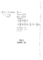
- FIG. 3 depicts an illustrative block diagram of an 8 bit-parallel bus symmetric line coding machine in accordance with the invention.
- OOK On-Off Keying
- the light from a laser is modulated such that a low amplitude signal represents one logical state (a “0” state, for instance), while a high amplitude signal represents another logical state (a “1” state).
- These two logical states representing the data bit values 0 and 1, are propagated along the transmission line repetitively once each clock period (sampling instant), T.
- Equipment at the receiving terminal detects the intensity of the light signal, reconstructs the clock, samples the light intensity at each clock interval, and decides whether a 0 or 1 data bit was transmitted.
- the electric field of the light modulated onto the optical fiber may be described according to its radio-frequency (“RF”) electric field envelope and the underlying optical carrier field.
- the envelope contains the RF field amplitude, together with the complex phase of the field.
- An OOK signal has an envelope that takes on values of 0 or 1 at each sampling instant. More complex line codes take on other values at each sampling instant. For instance, phase shift keying takes on values in the set ⁇ 1, +1 ⁇ , while Alternate Mark Inversion (“AMI”) takes on values in ⁇ 1,0, +1 ⁇ .
- AMI Alternate Mark Inversion
- the envelope may be represented as a data symbol multiplied into a unit modulation pulse.
- a Non-Return-to-Zero (“NRZ”) OOK signal may be represented as a full duty cycle modulation pulse, multiplied by a data amplitude in the set ⁇ 0,1 ⁇ . This may be expressed as the convolution of the unit modulation pulse with a train of impulses, each carrying a weight given by the data amplitude.
- the power spectrum of the light on the transmission fiber is determined from the RF envelope.
- the envelope is represented as the convolution of modulation pulse and data amplitude impulse train
- the power spectrum is simply the product of the Fourier transform of the modulation pulse and that of the impulse train.
- the transform of the impulse train is expressed in terms of its autocorrelation. For this reason, correlations in the data amplitudes introduce structure into the transmission power spectrum. It is control of these correlations, and the associated shaping of the power spectrum, that is the goal of line coding.
- the optical power spectrum of the transmission may be calculated from the autocorrelation of the line code.
- the line code power spectral density, S L ( ⁇ ), provides a means to control the spectrum of the transmission by controlling the correlations between output symbols. These relations demonstrate that spectral shaping may be effected without changing the modulation pulse itself.
- the intellectual property contained in this document will comprise invention of spectral shaping line codes, and their implementations, to control the spectrum of transmission of optical signals, and the mitigation of impairments suffered in propagating through optical fiber.
- the flat spectrum uses requires bandwidth out to very high frequencies, causing channels to be broadly spaced.
- the narrow spectral peaks, which result from the phase coherence of the light source, are problematic due to nonlinear propagation effects in optical fibers. Both of these issues are addressed by line coding.
- Each bit of the output symbol may be mapped onto the contacts of a Mach-Zehnder (“MZ”) modulator.
- the MZ modulator divides the incoming light into two waveguides, applies a variable and independent phase shift, ⁇ 1 and ⁇ 2 , to each, and recombines them at the output The effect is to generate an optical field at the output with electric field envelope proportional to E ⁇ [ exp( i ⁇ 1 )+exp( i ⁇ 2 )]/2.
- ⁇ 1 (v 1 +v 2 )/2
- ⁇ 2 ⁇ (v 1 +v 2 )/2
- Other alternatives include complementing either or both of the output bits, v 1 and v 2 .
- transitions in the output of the modulator may be effected by transitions of either of the two inputs, independently. This provides a means to reduce the frequency with which the two binary inputs make transitions. This translates directly into reduced requirements for the electronic and optical components.
- some method of signal processing is required to produce the correct signals, v 1 and V 2 , to be used to drive the modulator contacts. This method is line coding, a broad category of which will be described by symmetric line coding machines.
- the symmetric line coding machine of the present invention may be described in the following way.
- the unique input symbols form a set, ⁇ d 1 , . . . , d n ⁇ .
- For each input symbol there is associated a pair of output symbols, forming a set, ⁇ P 1 ,Q 1 ⁇ , . . . , ⁇ P n ,Q n ⁇ .
- Each time the machine receives an input symbol, d k it produces an output symbol from the appropriate set, ⁇ P k ,Q k ⁇ .
- the symbols P k and Q k may, or may not, be unique. For at least one k, P k and Q k must differ.
- the input symbol set be ⁇ d 1 , d 2 , d 3 ⁇
- the output set be ⁇ P 1 ,Q 1 ⁇ , ⁇ P 2 ,Q 2 ⁇ , ⁇ P 3 ,Q 3 ⁇ .
- the input symbol sequence is d 1 d 2 d 3 d 1 d 3 d 3 .
- the output sequence would be P 1 P 2 P 3 P 1 Q 3 Q 3 .
- the first output is P 1 , since it is the first instance of input d 1 .
- the second output is P 2 , since it is the first instance of input d 2 .
- the third output is P 3 , since it is the first instance of input d 3 .
- the fourth input is d 1 , so count the number of input symbols between this instance of d 1 and the most recent prior instance of d 1 , at which time output P 1 was produced.
- the fifth input is d 3 , for which there is one other symbol, d 1 , intervening between this input and the most recent prior input of d 3 , for which the output symbol was P 3 .
- the sixth input is d 3 , corresponding to output symbol Q 3 .
- the immediately prior input was d 3 , also, so there are zero other symbols intervening. Zero is not an odd number, so the output symbol is the same as for that input, Q 3 .
- the Bitstream symmetric line coding machines is a symmetric line coding machines in which each input symbol, d k , is a sequence of binary digits (bits). Likewise, each output is a sequence of bits.
- the Regular Bitstream symmetric line coding machine is a symmetric line coding machine in which each input symbol, d k , is a sequence of n bits, and each output symbol is a unique sequence of n+1 bits.
- the Complementary Regular Bitstream symmetric line coding machine is a symmetric line coding machine in which each input symbol, d k , is a sequence of n bits, each output symbol is a unique sequence of n+1 bits, and for each input symbols, d k , the two corresponding output symbols, P k and Q k , are bitwise complements of each other.
- FIG. 1 An illustrative embodiment of the Binary Complementary Regular Bitstream symmetric line coding machine is depicted in FIG. 1 .
- the binary input, d is processed to produce binary output pairs, (v 1 ,v 2 ).
- the symmetric line coding modulator in accordance with the invention, is the application of each of the output bits of a Binary Complementary Regular Bitstream symmetric line coding machine to the two contacts of a MZ modulator, as depicted in FIG. 2 .
- the two output bits are amplified by drive amplifiers, and the resulting signal applied to the contacts of the modulator.
- the power spectrum of the electrical signal applied to each contact of the modulator is described by Eq (3).
- the electric field envelope of the optical transmission is described by the ASI line code.
- the optical spectrum is also described by Eq. (3), so that a null is driven into the power spectrum of the transmitted light. This significantly lowers the high frequency content of the transmission, producing narrower channels, and allowing channels to be more closely spaced.
- a rule is established for identifying the sequence order of the inputs on each of the parallel input lines; at the output, a rule is established for identifying the sequence order of the outputs on each of the parallel output lines. Given these two rules, the contents of the input lines are processed to produce the contents of the output lines according to the operation of a symmetric line coding machine.
- the Bitstream parallel-symmetric line coding machine is a parallel-symmetric line coding machine in which each input symbol, d k , is a sequence of binary digits (bits). Likewise, each output is a sequence of bits.
- the Regular Bitstream parallel-symmetric line coding machine is a parallel-symmetric line coding machine in which each input symbol, d k , is a sequence of n bits, and each output symbol is a unique sequence of n+1 bits.
- the Complementary Regular Bitstream parallel-symmetric line coding machine is a parallel-symmetric line coding machine in which each input symbol, d k , is a sequence of n bits, each output symbol is a unique sequence of n+1 bits, and for each input symbols, d k , the two corresponding output symbols, P k and Q k , are bitwise complements of each other.
- An embodiment of a parallel symmetric line coding machine shown in FIG. 3 , teaches how to construct logic for an 8-bit parallel bus.
- the inputs labeled d 0 through d 7 , are processed to produce the outputs, labeled v 1 0 through v 1 7 and v 2 0 through v 2 7 .
- the output symbol pairs are (v 1 ,v 2 ).
- the ordering is first d 0 , next d 1 , . . . , finally (d 7 , and likewise on the output.
Landscapes
- Engineering & Computer Science (AREA)
- Computer Networks & Wireless Communication (AREA)
- Signal Processing (AREA)
- Physics & Mathematics (AREA)
- Spectroscopy & Molecular Physics (AREA)
- Optical Communication System (AREA)
- Dc Digital Transmission (AREA)
- Compression, Expansion, Code Conversion, And Decoders (AREA)
Priority Applications (5)
| Application Number | Priority Date | Filing Date | Title |
|---|---|---|---|
| US10/100,361 US6847312B2 (en) | 2001-03-19 | 2002-03-18 | Symmetric line coding |
| AU2002250395A AU2002250395A1 (en) | 2001-03-19 | 2002-03-19 | Symmetric line coding |
| EP02719305A EP1371201B1 (de) | 2001-03-19 | 2002-03-19 | Symmetrische leitungskodierung |
| PCT/US2002/008737 WO2002076052A2 (en) | 2001-03-19 | 2002-03-19 | Symmetric line coding |
| DE60229921T DE60229921D1 (de) | 2001-03-19 | 2002-03-19 | Symmetrische leitungskodierung |
Applications Claiming Priority (2)
| Application Number | Priority Date | Filing Date | Title |
|---|---|---|---|
| US27702601P | 2001-03-19 | 2001-03-19 | |
| US10/100,361 US6847312B2 (en) | 2001-03-19 | 2002-03-18 | Symmetric line coding |
Publications (2)
| Publication Number | Publication Date |
|---|---|
| US20020175837A1 US20020175837A1 (en) | 2002-11-28 |
| US6847312B2 true US6847312B2 (en) | 2005-01-25 |
Family
ID=26797067
Family Applications (1)
| Application Number | Title | Priority Date | Filing Date |
|---|---|---|---|
| US10/100,361 Expired - Fee Related US6847312B2 (en) | 2001-03-19 | 2002-03-18 | Symmetric line coding |
Country Status (5)
| Country | Link |
|---|---|
| US (1) | US6847312B2 (de) |
| EP (1) | EP1371201B1 (de) |
| AU (1) | AU2002250395A1 (de) |
| DE (1) | DE60229921D1 (de) |
| WO (1) | WO2002076052A2 (de) |
Cited By (2)
| Publication number | Priority date | Publication date | Assignee | Title |
|---|---|---|---|---|
| US20060083519A1 (en) * | 2004-10-20 | 2006-04-20 | Samsung Electronics Co.; Ltd | Chirped RZ-AMI optical transmitter |
| US20090289823A1 (en) * | 2008-05-23 | 2009-11-26 | Samsung Electronics Co., Ltd. & Industry- Academic Coorperation Foundation, Yonsei University | Sigma-delta analog-to-digital converter and solid-state image pickup device |
Families Citing this family (1)
| Publication number | Priority date | Publication date | Assignee | Title |
|---|---|---|---|---|
| DK3112327T3 (da) | 2015-06-30 | 2018-01-29 | Heidelbergcement Ag | Halvstive coatinger med øget greb og fremgangsmåde til deres fremstilling |
Citations (6)
| Publication number | Priority date | Publication date | Assignee | Title |
|---|---|---|---|---|
| US3678503A (en) * | 1970-07-06 | 1972-07-18 | Honeywell Inc | Two phase encoder system for three frequency modulation |
| US3815122A (en) * | 1973-01-02 | 1974-06-04 | Gte Information Syst Inc | Data converting apparatus |
| US4677319A (en) | 1983-06-25 | 1987-06-30 | Standard Telephones And Cables Public Limited Company | Electrical circuit for interfacing high frequency signals to the logic levels of any logic family having a switching voltage at the mean of the "0" and "1" voltages |
| EP0471130A1 (de) | 1990-08-16 | 1992-02-19 | International Business Machines Corporation | Kodierungsverfahren und Vorrichtung zur Pipeline- und Parallelverarbeitung |
| EP0543070A1 (de) | 1991-11-21 | 1993-05-26 | International Business Machines Corporation | Codierungsystem und -Verfahren, das quaternäre Codes anwendet |
| US5454006A (en) * | 1990-07-18 | 1995-09-26 | Unitex Ab | Method and apparatus for bandwidth limited binary signals |
-
2002
- 2002-03-18 US US10/100,361 patent/US6847312B2/en not_active Expired - Fee Related
- 2002-03-19 WO PCT/US2002/008737 patent/WO2002076052A2/en not_active Ceased
- 2002-03-19 AU AU2002250395A patent/AU2002250395A1/en not_active Abandoned
- 2002-03-19 DE DE60229921T patent/DE60229921D1/de not_active Expired - Fee Related
- 2002-03-19 EP EP02719305A patent/EP1371201B1/de not_active Expired - Lifetime
Patent Citations (8)
| Publication number | Priority date | Publication date | Assignee | Title |
|---|---|---|---|---|
| US3678503A (en) * | 1970-07-06 | 1972-07-18 | Honeywell Inc | Two phase encoder system for three frequency modulation |
| US3815122A (en) * | 1973-01-02 | 1974-06-04 | Gte Information Syst Inc | Data converting apparatus |
| US4677319A (en) | 1983-06-25 | 1987-06-30 | Standard Telephones And Cables Public Limited Company | Electrical circuit for interfacing high frequency signals to the logic levels of any logic family having a switching voltage at the mean of the "0" and "1" voltages |
| US5454006A (en) * | 1990-07-18 | 1995-09-26 | Unitex Ab | Method and apparatus for bandwidth limited binary signals |
| EP0471130A1 (de) | 1990-08-16 | 1992-02-19 | International Business Machines Corporation | Kodierungsverfahren und Vorrichtung zur Pipeline- und Parallelverarbeitung |
| US5177482A (en) * | 1990-08-16 | 1993-01-05 | International Business Machines Incorporated | Rll encoder and decoder with pipelined plural byte processing |
| EP0543070A1 (de) | 1991-11-21 | 1993-05-26 | International Business Machines Corporation | Codierungsystem und -Verfahren, das quaternäre Codes anwendet |
| US5331320A (en) * | 1991-11-21 | 1994-07-19 | International Business Machines Corporation | Coding method and apparatus using quaternary codes |
Cited By (4)
| Publication number | Priority date | Publication date | Assignee | Title |
|---|---|---|---|---|
| US20060083519A1 (en) * | 2004-10-20 | 2006-04-20 | Samsung Electronics Co.; Ltd | Chirped RZ-AMI optical transmitter |
| US7386239B2 (en) * | 2004-10-20 | 2008-06-10 | Samsung Electronics Co., Ltd. | Chirped RZ-AMI optical transmitter |
| US20090289823A1 (en) * | 2008-05-23 | 2009-11-26 | Samsung Electronics Co., Ltd. & Industry- Academic Coorperation Foundation, Yonsei University | Sigma-delta analog-to-digital converter and solid-state image pickup device |
| US7773018B2 (en) * | 2008-05-23 | 2010-08-10 | Samsung Electronics Co., Ltd. | Sigma-delta analog-to-digital converter and solid-state image pickup device |
Also Published As
| Publication number | Publication date |
|---|---|
| US20020175837A1 (en) | 2002-11-28 |
| EP1371201B1 (de) | 2008-11-19 |
| WO2002076052A3 (en) | 2003-01-09 |
| DE60229921D1 (de) | 2009-01-02 |
| EP1371201A2 (de) | 2003-12-17 |
| AU2002250395A1 (en) | 2002-10-03 |
| WO2002076052A9 (en) | 2003-03-06 |
| WO2002076052A2 (en) | 2002-09-26 |
Similar Documents
| Publication | Publication Date | Title |
|---|---|---|
| JP3027944B2 (ja) | 光デュオバイナリ信号光の生成方法および光送信装置 | |
| US5892858A (en) | Duobinary coding and modulation technique for optical communication systems | |
| JPH08139681A (ja) | 光送信装置および光伝送システム | |
| US7349636B2 (en) | Optical phase and intensity modulation with improved transmitters | |
| KR100557142B1 (ko) | Rz-ami 광송신기 모듈 | |
| EP1456976B1 (de) | Optische phasenmodulation | |
| US20020171903A1 (en) | Return-to-zero optical modulator with configurable pulse width | |
| US6522438B1 (en) | High-speed optical duobinary modulation scheme | |
| KR100492971B1 (ko) | 듀오바이너리 광 전송장치 | |
| US6847312B2 (en) | Symmetric line coding | |
| Fallahpour et al. | Experimental generation of a 64-QAM by optically aggregating three independent QPSK channels using nonlinear wave mixing of multiple Kerr comb lines | |
| JP2004312678A (ja) | デュオバイナリ光伝送装置 | |
| US20020109893A1 (en) | Methods and apparatus for generating return-to-zero optically encoded data stream | |
| US6542276B1 (en) | Method and apparatus for increasing the spectral efficiency of dense wavelength division multiplexed systems | |
| US7133621B1 (en) | Optical communication with phase encoding and phase shifting | |
| US7236702B2 (en) | Method and system for duobinary coding of optical signals | |
| JP3447965B2 (ja) | 光送信装置 | |
| US8750723B2 (en) | Generation of a full-rate optical duobinary signal using half-rate electrical binary signals | |
| EP1411658A2 (de) | Optischer MSK Sender | |
| JP3953934B2 (ja) | 符号変換回路、及び光送信回路 | |
| JP4080948B2 (ja) | 光送信回路および光受信回路 | |
| Mahmud et al. | Comparison between duo binary filter and delay-and-add technique of duobinary transmission in fiber optic communication system | |
| Uemura et al. | Novel method of duobinary signal generation with half-bitrate signal sources | |
| Rozorynov et al. | Development of modulation formats in optical fiber communication channel | |
| WO2005091534A1 (en) | An optical duobinary transmission system and method |
Legal Events
| Date | Code | Title | Description |
|---|---|---|---|
| AS | Assignment |
Owner name: KODEOS COMMUNICATIONS, NEW JERSEY Free format text: ASSIGNMENT OF ASSIGNORS INTEREST;ASSIGNORS:LENZ, GADI;STARK, JASON;REEL/FRAME:015042/0695;SIGNING DATES FROM 20020610 TO 20020614 |
|
| CC | Certificate of correction | ||
| FEPP | Fee payment procedure |
Free format text: PAT HOLDER NO LONGER CLAIMS SMALL ENTITY STATUS, ENTITY STATUS SET TO UNDISCOUNTED (ORIGINAL EVENT CODE: STOL); ENTITY STATUS OF PATENT OWNER: LARGE ENTITY |
|
| AS | Assignment |
Owner name: FINISAR CORPORATION, CALIFORNIA Free format text: ASSIGNMENT OF ASSIGNORS INTEREST;ASSIGNOR:KODEOS COMMUNICATIONS, INC.;REEL/FRAME:020548/0944 Effective date: 20080130 |
|
| FPAY | Fee payment |
Year of fee payment: 4 |
|
| FPAY | Fee payment |
Year of fee payment: 8 |
|
| REMI | Maintenance fee reminder mailed | ||
| LAPS | Lapse for failure to pay maintenance fees | ||
| STCH | Information on status: patent discontinuation |
Free format text: PATENT EXPIRED DUE TO NONPAYMENT OF MAINTENANCE FEES UNDER 37 CFR 1.362 |
|
| STCH | Information on status: patent discontinuation |
Free format text: PATENT EXPIRED DUE TO NONPAYMENT OF MAINTENANCE FEES UNDER 37 CFR 1.362 |
|
| FP | Lapsed due to failure to pay maintenance fee |
Effective date: 20170125 |
|
| AS | Assignment |
Owner name: II-VI DELAWARE, INC., DELAWARE Free format text: ASSIGNMENT OF ASSIGNORS INTEREST;ASSIGNOR:FINISAR CORPORATION;REEL/FRAME:052286/0001 Effective date: 20190924 |