US6825725B1 - Integrated power amplifier circuit - Google Patents
Integrated power amplifier circuit Download PDFInfo
- Publication number
- US6825725B1 US6825725B1 US10/607,123 US60712303A US6825725B1 US 6825725 B1 US6825725 B1 US 6825725B1 US 60712303 A US60712303 A US 60712303A US 6825725 B1 US6825725 B1 US 6825725B1
- Authority
- US
- United States
- Prior art keywords
- signal
- amplification stage
- output
- supply voltage
- amplifier circuit
- Prior art date
- Legal status (The legal status is an assumption and is not a legal conclusion. Google has not performed a legal analysis and makes no representation as to the accuracy of the status listed.)
- Expired - Lifetime, expires
Links
Images


Classifications
-
- H—ELECTRICITY
- H03—ELECTRONIC CIRCUITRY
- H03F—AMPLIFIERS
- H03F3/00—Amplifiers with only discharge tubes or only semiconductor devices as amplifying elements
- H03F3/189—High frequency amplifiers, e.g. radio frequency amplifiers
- H03F3/19—High frequency amplifiers, e.g. radio frequency amplifiers with semiconductor devices only
- H03F3/195—High frequency amplifiers, e.g. radio frequency amplifiers with semiconductor devices only in integrated circuits
-
- H—ELECTRICITY
- H03—ELECTRONIC CIRCUITRY
- H03F—AMPLIFIERS
- H03F1/00—Details of amplifiers with only discharge tubes, only semiconductor devices or only unspecified devices as amplifying elements
- H03F1/02—Modifications of amplifiers to raise the efficiency, e.g. gliding Class A stages, use of an auxiliary oscillation
- H03F1/0205—Modifications of amplifiers to raise the efficiency, e.g. gliding Class A stages, use of an auxiliary oscillation in transistor amplifiers
- H03F1/0211—Modifications of amplifiers to raise the efficiency, e.g. gliding Class A stages, use of an auxiliary oscillation in transistor amplifiers with control of the supply voltage or current
- H03F1/0216—Continuous control
- H03F1/0233—Continuous control by using a signal derived from the output signal, e.g. bootstrapping the voltage supply
-
- H—ELECTRICITY
- H03—ELECTRONIC CIRCUITRY
- H03F—AMPLIFIERS
- H03F1/00—Details of amplifiers with only discharge tubes, only semiconductor devices or only unspecified devices as amplifying elements
- H03F1/02—Modifications of amplifiers to raise the efficiency, e.g. gliding Class A stages, use of an auxiliary oscillation
- H03F1/0205—Modifications of amplifiers to raise the efficiency, e.g. gliding Class A stages, use of an auxiliary oscillation in transistor amplifiers
- H03F1/0261—Modifications of amplifiers to raise the efficiency, e.g. gliding Class A stages, use of an auxiliary oscillation in transistor amplifiers with control of the polarisation voltage or current, e.g. gliding Class A
-
- H—ELECTRICITY
- H03—ELECTRONIC CIRCUITRY
- H03F—AMPLIFIERS
- H03F1/00—Details of amplifiers with only discharge tubes, only semiconductor devices or only unspecified devices as amplifying elements
- H03F1/30—Modifications of amplifiers to reduce influence of variations of temperature or supply voltage or other physical parameters
-
- H—ELECTRICITY
- H03—ELECTRONIC CIRCUITRY
- H03F—AMPLIFIERS
- H03F3/00—Amplifiers with only discharge tubes or only semiconductor devices as amplifying elements
- H03F3/20—Power amplifiers, e.g. Class B amplifiers, Class C amplifiers
-
- H—ELECTRICITY
- H03—ELECTRONIC CIRCUITRY
- H03F—AMPLIFIERS
- H03F2200/00—Indexing scheme relating to amplifiers
- H03F2200/207—A hybrid coupler being used as power measuring circuit at the output of an amplifier circuit
-
- H—ELECTRICITY
- H03—ELECTRONIC CIRCUITRY
- H03F—AMPLIFIERS
- H03F2200/00—Indexing scheme relating to amplifiers
- H03F2200/447—Indexing scheme relating to amplifiers the amplifier being protected to temperature influence
-
- H—ELECTRICITY
- H03—ELECTRONIC CIRCUITRY
- H03F—AMPLIFIERS
- H03F2200/00—Indexing scheme relating to amplifiers
- H03F2200/451—Indexing scheme relating to amplifiers the amplifier being a radio frequency amplifier
-
- H—ELECTRICITY
- H03—ELECTRONIC CIRCUITRY
- H03F—AMPLIFIERS
- H03F2200/00—Indexing scheme relating to amplifiers
- H03F2200/504—Indexing scheme relating to amplifiers the supply voltage or current being continuously controlled by a controlling signal, e.g. the controlling signal of a transistor implemented as variable resistor in a supply path for, an IC-block showed amplifier
Definitions
- the invention relates to the field of amplifier circuits, and more specifically to the field of integrated power amplifier circuits.
- Typical power amplifier (PA) technologies utilize multiple integrated circuits in order to provide functionality for amplification, power output control and for stabilization of the PA output signal level due to supply voltage and temperature fluctuations.
- bias currents supplied to the RF signal amplification stages is are an important determinant of the performance of the amplification stages.
- a bias current supplied to the base of a bipolar transistor acting as a RF signal amplification stage is a major determinant of the amplification performance demonstrated by that bipolar transistor. Selecting and supplying the correct bias current is crucial to optimizing the RF signal amplification characteristics of any transistor amplifier.
- having control over the bias current supplied to the transistor amplifiers can enable more sophisticated schemes for optimizing the power output characteristics of the transistor amplifier. For example, one might detect output power from a power amplifier and choose to modify the bias current in response to the measured output power.
- figures of merit associated with the performance of power amplifiers that might be optimized using control over the bias current, such as bias current reduction at lower output powers to improve operating efficiency when RF-induced rectification currents are low.
- PAIC power amplifier integrated circuit
- a power amplifier circuit comprising: an input port for receiving a RF input signal; an output port for providing therefrom a RF output signal, the RF output signal being an amplified version of the RF input signal; a supply voltage input port for receiving a supply voltage; a voltage regulator circuit for receiving the supply voltage and for providing a regulated supply voltage; a first amplification stage having a first gain and for receiving one of a signal derived from the RF input signal and the RF input signal and for providing a first amplified RF signal, the first amplification stage coupled to the voltage regulator circuit for receiving the regulated supply voltage; and, a second amplification stage having a second gain and coupled to the first amplification stage for receiving one of a signal derived from the first amplified RF signal and the first amplified RF signal and coupled to the output port for providing the output signal thereto, the second amplification stage coupled to the supply voltage input port for receiving the supply voltage other than regulated by the voltage regulator circuit.
- a method of amplifying a RF input signal to form a RF output signal that is an amplified version of the RF input signal comprising the steps of: receiving the RF input signal; providing a first amplification stage having a first gain; providing a second amplification stage having a second gain; receiving a first supply voltage; regulating the first supply voltage to provide a regulated supply voltage; providing the regulated supply voltage to the first amplification stage; providing the first supply voltage to the second amplification stage; and, amplifying one of a signal derived from the received RF input signal and the received RF input signal using the first amplification stage having the first gain and the second amplification stage having the second gain to form the RF output signal.
- a power amplifier circuit comprising: an input port for receiving a RF input signal; an output port for providing therefrom a RF output signal, the RF output signal being an amplified version of the RF input signal; a supply voltage input port for receiving a supply voltage; a voltage regulator circuit for receiving the supply voltage and for providing a regulated supply voltage; a first amplification stage having a first gain for receiving one of a signal derived from the RF input signal and the RF input signal and for providing a first amplified RF signal, the first amplification stage coupled to the voltage regulator circuit for receiving the regulated supply voltage; a second amplification stage having a second gain for receiving one of a signal derived from the first amplified RF signal and the first amplified RF signal and coupled to the output port for providing the output signal thereto, the second amplification stage coupled to the supply voltage input port for receiving the supply voltage, the supply voltage provided to the second amplification stage and other than regulated by the voltage regulator circuit;
- a power amplifier circuit comprising: an input port for receiving a RF input signal; an output port for providing a RF output signal therefrom that is an amplified version of the RF input signal; a control port for receiving a control signal; a supply voltage input port for receiving a supply voltage; a temperature sensing circuit for sensing a temperature of the power amplifier circuit and for providing a temperature signal in dependence thereon; a voltage sensing circuit for sensing a potential of a voltage supply and for providing a sense signal in dependence thereon; a first amplification stage having a first gain for amplifying one of a signal derived from the RF input signal and the RF input signal to form a first amplified RF signal, the first amplification stage for receiving at least one of the temperature signal and the sense signal and the control signal and for varying the first gain in dependence thereon; and, a second amplification stage having a second gain for amplifying one of a signal derived from the first amplified RF signal and
- a method of operating a multi amplification stage amplifier circuit comprising the steps of: receiving of a control signal having a control signal magnitude; providing a first amplification stage having a first gain; receiving one of a signal derived from a RF input signal and a RF input signal for amplification using the first amplification stage; amplifying the one of a signal derived from the RF input signal and the RF input signal using the first amplification stage to form a first amplified RF signal, the amplifying of the one of a signal derived from the RF input signal and the RF input signal performed in conjunction with a step of compensating of the first amplification stage for at least two of temperature and supply voltage and control signal magnitude; providing a second amplification stage having a second gain; receiving of the first amplified RF signal using the second amplification stage; and, amplifying one of a signal derived from the first amplified RF signal and the first amplified signal using the second amplification stage
- a power amplifier circuit comprising: an input port for receiving a RF input signal; an output port for providing a RF output signal therefrom that is an amplified version of the RF input signal; a control port for receiving a control signal; a supply voltage input port for receiving a supply voltage; a temperature sensing circuit for sensing a temperature of the power amplifier circuit and for providing a temperature signal in dependence thereon; a voltage sensing circuit for sensing a potential of a voltage supply and for providing a sense signal in dependence thereon; a first amplification stage having a first gain and for amplifying one of a signal derived from the RF input signal and the RF input signal to form a first amplified signal, the first amplification stage for receiving at least one of the temperature signal and the sense signal and the control signal and for varying the first gain in dependence thereon; and, a second amplification stage having a second gain and for amplifying one of a signal derived from the first amplified signal the first amp
- a method of operating a poly stage amplifier circuit comprising the steps of: providing of a first amplification stage having a first gain and for receiving one of a signal derived from a RF input signal and a RF input signal for amplification; amplifying the one of a signal derived from the RF input signal and the RF input signal using the first amplification stage to form a first amplified signal, the amplifying of the one of a signal derived from the RF input signal and the RF input signal performed in conjunction with a step of compensating of the first amplification stage for at least one of temperature and supply voltage fluctuation and control signal magnitude; providing of a second amplification stage having a second gain and for receiving one of a signal derived from the first amplified signal and the first amplified signal; supplying the supply voltage to the second amplification stage without a substantial voltage drop between a potential of the supply voltage and that received by the second amplifying stage; and, amplifying the signal derived from the first
- an amplifier circuit for receiving an input signal for amplification comprising: an input port for receiving a RF input signal; an output port for providing a RF output signal therefrom that is an amplified version of the RF input signal; a control port for receiving a control signal; a supply voltage input port for receiving a supply voltage; a regulator circuit for receiving the supply voltage and for providing a regulated supply voltage in dependence upon at least one of a temperature of the amplifier circuit, the supply voltage, and the regulated supply voltage, where at least one of the temperature signal, the supply voltage and the regulated supply voltage are provided to the regulator circuit using a direct feedback path; at least a first amplification stage and a second amplification stage, the at least a first amplification stage and the second amplification stage coupled to at least one of the supply voltage and the regulated supply voltage, the first amplification stage for receiving one of a signal derived from the RF input signal and the RF input signal and for providing a first amplified signal, to the second
- a method of operating a multi stage amplifier circuit comprising the steps of: receiving a RF input signal; receiving a supply voltage; receiving a control signal; receiving at least one of a temperature signal related to a temperature of the amplifier circuit and a sense signal related to the supply voltage; regulating the received supply voltage to form a regulated supply voltage in dependence upon the received at least one of temperature signal and sense signal; providing a first amplification stage having a first gain; providing a second amplification stage having a second gain; providing the regulated supply voltage to at lease one of the first amplification stage and the second amplification stage; and, amplifying one of a signal derived from the received RF input signal and the received RF input signal using the first amplification stage and the second amplification stage to form a RF output signal that is an amplified version of the one of a signal derived from the received RF input signal and the RF input signal.
- FIG. 1 illustrates a prior art utilizing a power amplifier circuit, an external feedback circuit and an external output power detection circuit
- FIG. 2 illustrates a prior art PA circuit utilizing a voltage regulation circuit for controlling an output power of a RF output signal emitted from the PA;
- FIG. 3 illustrates a PA circuit that utilizes an external current sensing circuit
- FIG. 4 illustrates a first embodiment of the invention, a Dual Feedback-Low power regulation circuit for a three stage PAIC;
- FIG. 5 illustrates a second embodiment of the invention, a three stage RF PA formed in a PAIC with a current source feedback circuit having low RF output signal power regulation;
- FIG. 6 illustrates a third embodiment of the invention, a three stage RF PA formed in a PAIC die in conjunction with an integrated logarithmic detector circuit, integrated into the same die.
- FIG. 1 illustrates a prior art power amplifier (PA) integrated circuit (IC) (PAIC) 101 , a comparator circuit 102 , and a RF power detection circuit 103 .
- the PAIC 101 has an input port 101 a for receiving a RF input signal, an output port 101 b for providing a RF output signal therefrom, a supply voltage input port 101 d for receiving a supply voltage and a control port 101 c for receiving a control signal.
- Disposed within the PAIC 101 are a first amplification stage 121 , a second amplification stage 122 , and a third amplification stage 123 .
- Each amplification stage comprises a transistor having a base terminal coupled to one of an input port and a collector terminal of a previous amplification stage using a capacitor.
- Capacitor 131 is used to couple the RF input signal to the first amplification stage
- capacitors 132 , 133 are used to couple the amplification stages together.
- the first amplification stage 121 has disposed therein a first current source 111
- the second amplification stage 122 has disposed therein a second current source 112
- the third amplification stage has disposed therein a third current source 113 .
- the first, second and third current sources arc for providing first, second and third bias currents to first, second and third amplification stages.
- the first, second and third currents are provided to the base terminals of the first, second and third transistors disposed within the three amplification stages, respectively.
- An integrated temperature sensing circuit (ITSC) 104 is integrated within the PAIC 101 for sensing a temperature of the die having the PAIC 101 disposed therein and for providing a first temperature signal therefrom, in response to a temperature of the die on which the power amplifier circuit is formed.
- the first temperature signal is provided to the first current source 111 , second current source 112 and third current source 113 .
- the control input port 101 c is coupled to each of the current sources, such that the current sources each receive the control signal therefrom.
- Each current source is for varying its current provided to its corresponding amplification stage in dependence upon the control signal and the first temperature signal.
- Each amplification stage is disposed between the supply voltage input port 101 d and a ground potential.
- a transistor is disposed in each amplification stage with its collector terminal coupled to the supply voltage input port 101 d and the emitter terminal thereof coupled to ground.
- the transistor disposed within the third amplification stage 123 has its collector terminal coupled to the output port 101 b and its base terminal capacitvely coupled to the collector terminal of the transistor disposed within the second amplification stage.
- the transistor disposed in the first amplification stage has its base terminal capacitvely coupled to the input port 101 a using capacitor 131 .
- the output port 101 b is additionally coupled to the supply voltage input port 101 d.
- the PAIC 101 is formed on a GaAs substrate, while the RF power detection circuit 103 having a detector diode 105 disposed therein for receiving a portion of the RF output signal current emitted from the PAIC output port 101 b, is formed on a silicon substrate.
- the comparator circuit 102 is formed on a silicon substrate, or on an FR4 glass-fiber type substrate, and is for receiving a diode output voltage proportional to RF output signal power.
- at least three different substrates are utilized for implementing of the PAIC 101 , the RF power detection circuit, and the feedback circuit 102 .
- the bias current sources, and temperature sensing circuits are often disposed upon another substrate. Thus, bondwires between the substrates are required in the finished device, which increases associated manufacturing costs.
- the diode output voltage is compared to a target signal and the comparator circuit 102 provides the control to the control port 101 c of the PAIC 101 in response thereto.
- the PAIC 101 amplifies the RF input signal based upon a gain of each amplification stage to provide the RF output signal.
- a second prior art architecture implements an off-chip voltage regulator circuit 202 for controlling an output power of a RF output signal.
- a power amplifier integrated circuit 201 is provided with an input port 201 a for receiving a RF input signal, an output port 201 b for providing a RF output signal therefrom, and a regulated voltage input port 201 c for receiving a regulate positive supply voltage from the off-chip voltage regulator circuit 202 .
- the regulator circuit 202 has a supply voltage input port 202 b for receiving a supply voltage from a power supply (not shown) coupled thereto.
- a control port 202 a is disposed on the regulator circuit 202 for receiving a control signal.
- an operational amplifier (OpAmp) 203 having a first input port coupled with the control port 202 a for receiving the control signal and an output port of the OpAmp 203 is coupled to a gate terminal of a FET 204 .
- a difference amplifier is disposed in a similar manner to the OpAmp 203 and replaces the OpAmp 203 .
- Drain and source terminals of the FET 204 are disposed in series between the positive supply voltage input port 202 b and a regulated supply voltage output port 202 c.
- a feedback sense circuit 205 is disposed between a second input port of the OpAmp 203 and the regulated supply voltage output port 202 c.
- the regulated supply voltage output port 202 c is coupled to the regulated supply voltage input port 201 c for receiving the regulated supply voltage from the regulator circuit 202 .
- each amplification stage comprises a transistor having a base terminal coupled to one of an input port and a collector terminal of a previous amplification stage.
- the amplification stages are capacitively coupled using capacitors 231 , 232 , 233 .
- Capacitor 231 is used to couple the RF input signal to the first amplification stage 221 .
- first amplification stage 221 has disposed therein a first current source 211
- second amplification stage 222 has disposed therein a second current source 212
- third amplification stage has disposed therein a third current source 213 .
- An integrated temperature sensing circuit (ITSC) 204 is integrated within the PAIC die 201 for sensing a temperature of the die of the PAIC 201 and for providing a first temperature signal in response to the temperature of the die. The first temperature signal is provided to the first current source 211 , the second current source 212 and third current source 213 .
- ITSC integrated temperature sensing circuit
- Each current source is for varying its bias current provided to each amplification stage in dependence upon the received first temperature signal.
- Each amplification stage is disposed between the regulated supply voltage input port 201 c, for receiving the regulated supply voltage from the regulator circuit 202 , and a ground potential.
- Each transistor within each amplification stage has its collector terminal coupled to the regulated supply voltage input port 201 c and the emitter terminal thereof coupled to ground.
- the transistor forming the third amplification stage 223 has its collector terminal coupled to the PAIC output port 201 b.
- the base terminal of the transistor disposed within the first amplification stage 221 has its base terminal capacitvely coupled to the PAIC input port 201 a using capacitor 231 .
- the PAIC output port 201 b is additionally coupled to the to the reduced positive supply voltage input port 201 c.
- the regulator IC 202 employs a low drop out (LDO) regulator circuit in series with a collector terminal of the transistors disposed within the amplification stages of the PAIC 201 .
- the FET 204 disposed within the regulator circuit is typically in the form of a silicon PMOS transistor, which in conjunction with the OpAmp 203 , provides specific bandwidth compensated regulated supply voltage to the amplification stages of the PAIC 201 .
- the amplification stages of the PAIC are typically formed on a separate GaAs substrate from the regulator circuit 202 .
- the regulator IC 202 Due to the high saturation current and low ON resistance requirements of the regulator IC 202 for providing a low resistance signal path to the collector terminals of the transistors forming each of the amplification stages, a large area PMOS die is utilized for implementing of the regulator IC 202 , resulting in a high manufacturing cost and a high overall module size. Unfortunately, with the size of the regulator circuit IC 202 and regulator IC circuit technology requirements, along with the poor thermal isolation characteristics of the amplification stages, the regulator IC 202 is prevented from being integrated on the same die as the PAIC 202 .
- FIG. 3 A third prior art architecture, which utilizes an off-chip current sense IC 302 for sensing current consumed by circuit elements forming the PAIC 301 , is illustrated in FIG. 3 .
- the sense IC 302 is on a separate die than the PAIC 301 .
- An input port 301 a is formed on the PAIC 301 for receiving a RF input signal
- an output port 301 b is provided for providing an amplified version of the input signal in the form of an amplified RF output signal therefrom
- a voltage input port 301 d is disposed on the PAIC for receiving a supply voltage from a power supply (not shown) connected thereto.
- the current sense IC 302 is provided with a supply voltage input port 302 a for receiving a voltage from a power supply (not shown) coupled thereto.
- a sense resistor 304 is disposed between the voltage input port 302 a and a reduced voltage output port 302 c.
- the reduced voltage output port 302 c is coupled to the output port 301 b of the PAIC for providing a reduced supply voltage to the third amplification stage.
- a differential sensing amplifier 303 is disposed within the sense IC 302 and has its input ports disposed in parallel with the sense resistor 304 for measuring a voltage drop thereof.
- An output port of the differential sensing amplifier 303 is coupled to a sense signal output port 302 b for providing a sense signal therefrom.
- a third amplification stage 323 draws more current, the voltage drop across the sense resistor increases.
- a sense signal input port 301 e is also provided for coupling off-chip to the sense signal output port 302 b.
- Disposed within the PAIC 301 are a first amplification stage 321 , a second amplification stage 322 and the third amplification stage 323 .
- each amplification stage comprises a transistor having a base terminal capacitively coupled to one of an input port and a collector terminal of a previous amplification stage.
- Capacitors 331 , 332 , 333 are provided for facilitating capacitive coupling of the amplification stages.
- Capacitor 331 is disposed for coupling the RF input signal to the first amplification stage.
- each amplification stage has disposed therein a first current source 311 , a second current source 312 and a third current source 313 , for providing first, second and third bias currents.
- the first, second and third bias currents are provided to the base terminals of first, second and third transistors disposed within the three amplification stages.
- An integrated temperature sensing circuit (ITSC) 304 is integrated within a die of the PAIC 301 for sensing a temperature of the die and for providing a first temperature signal in response to the temperature of the die.
- the first temperature signal is provided to the first current source 311 , second current source 312 and third current source 313 .
- the control port 301 c is coupled to each of the current sources for receiving the control signal.
- Each current source is for varying the current provided to a respective amplification stage in dependence upon the received temperature signal, the control signal received from a control port 301 c, and a sense signal received from the off chip sense IC 302 via the sense signal input port 301 e.
- the first amplification stage 321 and the second amplification stage 322 are disposed between the positive supply voltage input port 301 d, for receiving a positive supply voltage from the power supply (not shown) coupled thereto, and ground.
- a second transistor disposed within the second amplification stage 322 has its collector terminal capacitively coupled, using capacitor 333 , to the base terminal of the third transistor disposed within the third amplification stage 323 .
- a collector terminal of a third transistor disposed within the third amplification stage 323 is coupled to the output port 301 b and to the reduced voltage output port 302 c.
- a first limitation lies in that a voltage drop realized across the sense resistor 304 disposed in the sense IC 302 results in the sensing IC 302 having a loss in operating efficiency for the PAIC 301 for all RF output signal power levels.
- the sense resistor 304 has a low resistance value such that a substantial voltage drop is not realized between the DC potential provided to the collector terminals of the transistors and the DC potential provided to the PAIC output port 301 b.
- both tolerance and dynamic range issues associated therewith are relevant to PAIC performance.
- the manufacturing tolerance results in differences in detected output signal power levels for a given control voltage from one manufactured sense IC unit to another.
- the small resistance value additionally affects output signal power accuracy at low output signal power levels due to the extremely small voltage drop realized across the sense resistor 304 and the ability of the differential sensing amplifier 303 to measure this voltage drop accurately.
- a different magnitude sense signal results due to the manufacturing difference in the sense resistances.
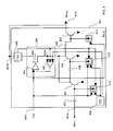
- FIG. 4 illustrates a Dual Feedback-Low power regulation circuit for a three-stage power amplifier integrated circuit (PAIC) 401 in accordance with a first embodiment of the invention.
- the PAIC 401 preferably has integrated therein a regulator circuit 405 , in the form of a reduced die area regulator circuit, which is formed within the same die as the PAIC 401 .
- the PAIC 401 is provided with an input port 401 a for receiving a RF input signal, an output port 401 b for providing a RF output signal, in the form of an amplified version of the RF input signal therefrom, a supply voltage input port 401 d for receiving a supply voltage, and a control port 401 c for receiving a control signal from an external source (not shown).
- a voltage sensing circuit 406 is preferably disposed in series between the voltage input port 401 d and the integrated regulator circuit 405 , where the integrated regulator circuit is preferably in the form of an integrated compact low dropout (LDO) voltage regulator circuit.
- the voltage sensing circuit 406 is integrated on the same die as the PAIC 401 .
- the integrated regulator circuit 405 receives the supply voltage from the voltage input port 401 d and provides a regulated supply voltage therefrom.
- the voltage sensing circuit 406 provides a voltage sense signal in dependence upon a sensed potential of the supply voltage.
- an operational amplifier (OpAmp) 403 having a first input port coupled with the control port 401 c for receiving the control signal.
- the OpAmp is replaced with a difference amplifier.
- An output port of the OpAmp 403 is coupled to a gate terminal of a FET 404 .
- the FET 404 drain and source terminals are disposed in series between the voltage sensing circuit 406 and the junction 404 a formed at the collector terminals of a first transistor disposed within a first amplification stage 421 and a second transistor disposed within a second amplification stage 422 .
- a second input port of the OpAmp 403 is coupled to an output port of a first summing circuit 407 .
- a first input port of the first summing circuit 407 is for coupling to the junction 404 a formed between one of the drain and source terminals of the FET 404 and the collector terminals of the first and second transistors disposed within the first and second amplification stages, 421 and 422 , respectively.
- a second input port of the first summing circuit 407 is for receiving the voltage sense signal from the voltage sensing circuit 406 .
- Junction 404 a receives the regulated supply voltage from the integrated regulator circuit 404 .
- each amplification stage comprises a transistor having a base terminal coupled to one of an input port and a collector terminal of a previous amplification stage, using capacitive coupling.
- Capacitors 431 , 432 , 433 are provided for facilitating the capacitive coupling.
- Capacitor 431 is disposed between the input port 401 a and the first amplification stage 421 for capacitively coupling of the RF input signal into the PAIC 401 , and second and third capacitors 432 and 433 act to capacitively couple the second and third amplification stages together. Additionally, the three amplification stages have disposed therein a first current source 411 , a second current source 412 and third current source 413 , for providing first, second and third bias currents to the base terminals of first, second and third transistors, respectively. The three amplification stages are thus provided with first, second and third gains, respectively, in response to the first, second and third bias currents.
- An integrated temperature sensing circuit (ITSC) 408 is integrated within the same die as the PAIC 401 and is for sensing a temperature of the die and for providing an at least a temperature signal in response to a temperature thereof.
- the at least a temperature signal is in the form of a first temperature signal and a second temperature signal, where the first temperature signal is provided to the first current source 411 and to the second current source, and where the second temperature signal is provided to a third input port of the first summing circuit 407 .
- the PAIC output port 401 b is additionally coupled to the positive voltage input port 401 d for receiving a DC bias voltage for biasing of the third transistor collector terminal.
- the first, second and third current sources are additionally coupled to the control port 401 c for receiving the control signal.
- the first current source 411 and the second current source 412 are for varying their bias current provided to the first and second amplification stages in dependence upon the received first temperature signal, the voltage sense signal, and the control signal.
- the third current source 413 is coupled to the control port 401 c for preferably having its magnitude varied only in response to the control signal.
- an indirect feedback loop is employed, which compensates the first and second amplification stages for temperature in order to maintain a fixed RF output signal power at the output port 401 b.
- the temperature of the PAIC die increases in response to the power dissipated by the third amplification stage. This change in temperature is reflected in the first and second temperature signals generated by the ITSC 408 .
- the first and second amplification stages provide a precompensated signal to an input port of the third amplification stage in order to precompensate the input signal to the third amplification stage for both power supply variations and PAIC die temperature variations.
- the precompensated signal provided to the third amplification stage is reflective of this heating.
- a control signal in the form of a ramp voltage is applied to the control port 401 c.
- the control signal is for achieving a desired target RF output signal power by controlling the first, second and third gains of the amplification stages within the PAIC 401 .
- the ramp voltage provides wide dynamic range performance for the PAIC 401 by varying the gain of the multi-stage PAIC through two means.
- the primary means of gain control is through variation of the regulated supply voltage provided to junction 404 a, based on the control signal received from the control port 401 c.
- the secondary means of gain variation is achieved through modification of the bias currents provided from each of the three current sources 411 , 412 , and 413 , where the three bias currents are proportional to a parameter of the control signal received at the control port 401 c.
- Regulator circuit 405 control of the first amplification stage 421 and second amplification stage 422 provides precise RF signal power control proportional to the square of the voltage on the collector terminals of the first and second transistors.
- This precisely controlled RF signal power is incident on the third amplification stage 423 and further amplified using the third amplification stage, in a controlled manner, through the action of third current source 413 and third transistor 423 .
- the presence of the regulator circuit 405 results in RF signal power emitted from the first and second amplification stages to be precisely known and independent of supply voltage variations occurring at the supply voltage input port 401 d.
- the sense circuit 406 is employed, which provides the sense signal to the first summing circuit 407 disposed in the regulator circuit 405 .
- the input signal provided to the third amplification stage reduces the low dropout (LDO), which maintains the gain of the third stage constant.
- Sensing the temperature of the PAIC die provides a further compensation factor for the regulator circuit 405 . Sensing the temperature removes temperature variation from the RF signal power incident at the third amplification stage 423 . Additionally, by optionally providing the temperature signal to the first and second current sources, fine-tuning of the temperature and voltage effects of the PAIC 401 are achieved.
- RF input signal power provided to the third amplification stage is continuously compensated in order to maintain a desired RF output signal power by varying the first and second bias currents as well as the collector terminal voltages using the regulator circuit 405 .
- the third stage transistor base current is slowly varied proportional to the control signal ramp voltage in order to minimize consumed current at low signal powers and to adequately drive the base terminal at high powers, thus achieving the desired dynamic range.
- the substantial reduction in the die area results from a smaller area FET 404 that is utilized within the regulator circuit 405 .
- the FET 404 is of a smaller size because only the first and second amplification stages are regulated using the regulated supply voltage and not the higher-powered third amplification stage. In regulating the supply voltage to the third amplification stage, much larger area FET devices are used in order to handle the higher power requirements of this third amplification stage.
- the third, or final amplification stage typically has a regulated supply voltage provided thereto.
- FIG. 5 illustrates a current source feedback circuit having low RF output signal power regulation for a three stage power amplifier integrated circuit (PAIC) 501 in accordance with a second embodiment of the invention.
- the PAIC 501 preferably has integrated therein a regulator circuit 505 , in the form of a reduced die area regulator circuit, which is formed within a same substrate as the PAIC 501 .
- the PAIC 501 is provided with a PAIC input port 501 a for receiving a RF input signal, a PAIC output port 501 b for providing an amplified RF output signal therefrom, a voltage input port 501 d for receiving a supply voltage, and a control port 501 c for receiving a control signal from an external source (not shown).
- a voltage sense circuit 506 is preferably integrated on the same die with the PAIC 501 and disposed in series between the supply voltage input port 501 d and the integrated regulator circuit 505 .
- the integrated regulator circuit 505 receives the supply voltage through the supply voltage input port 501 d and provides a regulated supply voltage therefrom.
- the voltage sensing circuit 506 provides a sense signal therefrom.
- an operational amplifier (OpAmp) 503 having a first input port coupled with the control port 501 c for receiving the control signal.
- the OpAmp is replaced with a difference amplifier.
- An output port of the OpAmp 503 is coupled to a gate terminal of a FET 504 .
- the FET drain and source terminals are disposed in series between the voltage sense circuit 506 and a junction 504 a formed between a collector terminal of a first transistor disposed within a first amplification stage 521 and a second transistor is disposed within a second amplification stage 522 .
- a second input port of the OpAmp 503 is coupled to an output port of a feedback sense circuit 507 .
- An input port of the feedback sense circuit 507 is coupled to the junction formed between the collector terminals of the first and second transistors disposed within a first amplification stage and a second amplification stage, respectively, and one of the gate and drain terminals of the FET 504 .
- a third amplification stage 523 is disposed within the PAIC 501 and integrated therewith on the same die.
- Each amplification stage comprises a transistor having a base terminal coupled to one of an input port and a collector terminal of a previous amplification stage using a capacitive coupling.
- Capacitors 531 , 532 , 533 are provided for facilitating the capacitive coupling.
- Capacitor 531 is disposed between the input port 501 a and the first amplification stage 521 for capacitively coupling of the RF input signal to the first amplification stage.
- the amplification stages have respectively disposed therein a first current source 511 , a second current source 512 and a third current source 513 , for providing first, second and third bias currents to the base terminals of first, second and third transistors, respectively.
- the three amplification stages are thus provided with first, second and third gains, respectively, in response to the first, second and third bias currents.
- An integrated temperature sensing circuit (ITSC) 508 is integrated within the die of the PAIC 501 for sensing a temperature of the die and for providing at least a temperature signal therefrom in response to a temperature of the die.
- the at least a temperature signal is in the form of a first temperature signal, where the first temperature signal is provided to the first current source 511 , the second current source 512 , and the third current source 513 .
- the third current source 513 is additionally coupled to the control port 501 c for receiving the control signal and to the voltage sense circuit 506 for receiving the voltage sense signal.
- the output port 501 b is additionally coupled with the supply voltage input port 501 d for receiving a DC bias voltage therefrom for the collector terminal of the third transistor disposed within the third amplification stage 523 .
- the first and second current sources are for varying their first and second bias current provided to the first and second amplification stages in dependence upon the received first temperature signal.
- the third current source is for varying its third bias current in dependence upon the first temperature signal, the control signal and the voltage sense signal.
- a direct feedback path is employed for providing the temperature signal to all three current sources.
- the first and second amplification stages receive the regulated supply voltage.
- the first and second amplification stages provide a partially precompensated signal to the third amplification stage.
- the temperature of the PAIC die increases in response to the power dissipated by the third amplification stage. This change in temperature is reflected in the temperature signal generated by the ITSC 508 .
- This embodiment also employs a similar technique for compensating of the RF output signal propagating from the third stage as disclosed in the first embodiment, but additionally utilizes a feedback signal, in the form of the voltage sense signal.
- a ramp voltage is applied to the control port 501 c for controlling a magnitude of the third current provided from the third current source 513 to the third amplification stage 523 .
- the voltage sense signal is additionally provided to the third current source for compensating the RF output signal emitted from the third amplification stage for supply voltage variations.
- a control signal in the form of a ramp voltage is applied to the control port 501 c.
- the control signal is used for achieving a desired target RF output signal power by controlling the first, second and third gains of the amplification stages within the PAIC 501 .
- the ramp voltage provides wide dynamic range performance for the PAIC 501 by varying the gain of the multi-stage PAIC through two means.
- the primary means of gain control is through variation of the regulated supply voltage provided to junction 504 a, based on the control signal received from the control port 501 c.
- the secondary means of gain control is achieved through modification of the bias currents provided from each of the three current sources 511 , 512 , and 513 , where the three bias currents are proportional to a parameter of the control signal.
- Regulator circuit 505 control of the first amplification stage 521 and second amplification stage 522 provides precise output power control proportional to the square of the voltage on the collector terminals of the first and second transistors.
- This precisely controlled RF signal power is incident on the third amplification stage 523 and further amplified using the third amplification stage in a controlled manner through the action of third current source 513 and third transistor 523 .
- the presence of the regulator circuit 505 results in output signal power emitted from the first and second amplification stages to be precisely known and independent of supply voltage variations occurring at the supply voltage input port 501 d.
- the sense circuit 506 is employed, which provides the sense signal to the third current source 513 for fine tuning of the third gain.
- the input signal provided to the third current source reduces the required size of the regulator circuit 505 in the form of a low dropout (LDO) circuit, and maintains the gain of the third stage constant.
- Sensing the temperature of the PAIC die provides a final compensation factor for three current sources. Sensing the temperature removes temperature variation from the RF signal power emitted from the output port 501 b.
- This circuit implementation of the second embodiment advantageously results in a substantial reduction in die and module size.
- the substantial reduction in the die area results from a smaller area FET that is utilized within the regulator circuit.
- the FET is of a smaller size because only the first and second amplification stages are regulated using the regulated supply voltage and not the higher-powered third amplification stage. Because of reduced current requirements of the first and second amplification stages, the regulator circuit occupies a small die area. It is known to those of skill in the art that in regulating the supply voltage to the third amplification stage, a much larger die area FET is used in order to handle the higher power requirements of the third amplification stage.
- the second embodiment offers simplified calibration requirements, reduced thermal load, and improved amplification efficiency at reduced RF output signal power levels.
- FIG. 6 illustrates a detector circuit, in the form of an integrated logarithmic detector circuit 610 , disposed in conjunction with a three stage power amplifier integrated circuit (PAIC) 601 in accordance with a third embodiment of the invention.
- the third embodiment of the invention has an integrated regulator circuit 605 , in the form of a reduced die area regulator circuit, which is formed in a same substrate as the PAIC 601 .
- the PAIC 601 is provided with an input port 601 a for receiving a RF input signal, a PAIC output port 601 b is for providing an amplified version of the RF input signal in the form of a RF output signal.
- a supply voltage input port 601 d is provided for receiving a supply voltage, and a control port 601 c is disposed therein for receiving a control signal from an external source (not shown).
- the integrated regulator circuit 605 is preferably integrated with the PAIC 601 and coupled to the supply voltage input port 601 d for receiving a supply voltage therefrom from a power supply (not shown) coupled thereto.
- the integrated regulator circuit 605 provides a regulated supply voltage therefrom to a junction 604 a.
- an operational amplifier (OpAmp) 603 having a first input port coupled with the control port 601 c for receiving the control signal.
- An output port of the OpAmp 603 is coupled to a gate terminal of a FET 604 .
- the FET drain and source terminals are disposed in series between the supply voltage input port 601 d and collector terminals of a junction 604 a formed between collector terminals of a first transistor disposed within a first amplification stage 621 and a second transistor disposed within a second amplification stage 622 .
- a second input port of the OpAmp 603 is coupled to an output port of a feedback sense circuit 607 .
- An input port of the feedback sense circuit 607 is coupled to the junction 604 a formed between the collector terminals of the first and second transistors and one of the source and drain terminals of the FET 604 .
- each amplification stage comprises a transistor having a base terminal coupled to one of an input port and a collector terminal of a previous amplification stage, using a capacitive coupling.
- Capacitors 631 , 632 , 633 are provided for facilitating the capacitive coupling.
- Capacitor 631 is disposed between the input port 601 a and the first amplification stage 621 for capacitively coupling of the RF input signal to the first amplification stage 621 .
- first, second and third amplification stages have disposed therein a first current source 611 , a second current source 612 and a third current source 613 , respectively, for providing first, second and third bias currents to the base terminals of first, second and third transistors disposed within amplification stages.
- An integrated temperature sensing circuit (ITSC) 608 is integrated within the PAIC die 601 for sensing a temperature of the PAIC die 601 and for providing a temperature signal.
- the temperature signal is provided to the first current source 611 , the second current source 612 , and to the third current source 613 .
- the third current source 613 is additionally coupled to the control port 601 c for receiving the control signal.
- the output port 601 b is additionally coupled with the supply voltage input port 601 d for receiving a DC bias voltage therefrom, where this DC bias is provided to a collector terminal of the third transistor disposed within the third amplification stage 623 .
- the integrated logarithmic detector circuit 610 is coupled to the PAIC output port 601 b for receiving a portion of current from the RF output signal. Disposed within the integrated logarithmic detector circuit 610 is a second summing circuit 609 having first, second and third input ports and an output port. The output port of the second summing circuit 609 is coupled to the third current source for providing a feedback signal in the form of an output level signal thereto.
- a first difference amplifier 641 is disposed in the integrated logarithmic detector circuit 610 with an output port thereof coupled to the first input port of the second summing circuit 609 . Disposed between the input ports of the first difference amplifier circuit 641 is a first sense resistor 651 , where a first input port of the first difference amplifier circuit 641 is coupled to the PAIC output port 601 b and a second input port of the first difference amplifier circuit 641 is coupled to a collector terminal of a first sense transistor 661 with an emitter terminal thereof coupled to ground. A base terminal of the first sense transistor 661 is coupled to a base terminal of a current mirror transistor 660 having a collector terminal coupled to the PAIC output port 601 b and an emitter terminal thereof coupled to ground.
- a second difference amplifier circuit 642 is disposed in the integrated logarithmic detector circuit 610 with an output port thereof coupled to the second input port of the second summing circuit 641 . Disposed between the input ports of the second difference amplifier 642 is a second sense resistor 652 , where a first input port of the second difference amplifier is coupled to the PAIC output port 601 b and a second input port of the second difference amplifier 642 is coupled to a collector terminal of a second sense transistor 662 with an emitter terminal thereof coupled to ground. A base terminal of the second sense transistor 662 is also coupled to the base terminal of the current mirror transistor 660 .
- a third difference amplifier circuit 643 is disposed in the integrated logarithmic detector circuit 610 with an output port thereof coupled to the third input port of the second summing circuit 641 . Disposed between the input ports of the third difference amplifier 643 is a third sense resistor 653 , where a first input port of the third difference amplifier 643 is coupled to the PAIC output port 601 b and a second input port of the third difference amplifier 642 is coupled to a collector terminal of a third sense transistor 663 with an emitter terminal thereof coupled to ground. A base terminal of the third sense transistor 663 is also coupled to the base terminal of the current mirror transistor 660 .
- the first and second current sources are for varying their bias current provided to the first and second transistors disposed in the first and second amplification stages in dependence upon the temperature signal.
- the third current source is for varying its third bias current in dependence upon the temperature signal, the control signal, and the feedback signal received from the integrated logarithmic detector circuit 610 .
- the third embodiment advantageously adds a direct feedback loop based upon RF output signal power detection from the output port 601 b.
- a voltage regulator circuit provides a regulated supply voltage to the first and second amplification stages to one of the collector and drain terminals of the transistors thereof to compensate for RF signal level changes in supply voltage of the third amplification stage.
- the first and second amplification stages are provided with a regulated supply voltage that offers stability during supply voltage variation.
- the third embodiment utilizes the DC coupled sense transistors 661 , 662 , and 663 , and the current mirror transistor 660 , selectively embedded in the integrated logarithmic detector circuit 610 , to “sense” a portion of the collector current of the third transistor disposed in the third amplification stage 623 .
- the sensed collector current is proportional to RF output signal power.
- Each of the three current mirror circuits utilizing first, second and third feedback transistors receive input voltages that are proportional to the output RF signal power.
- the three current mirror circuits utilizing sense transistors 661 , 662 , and 663 , employ sense resistors 651 , 652 , 653 that differ by 3 decades in order to provide RF output signal power sensitivity over a broad dynamic range of operation of the three stage PAIC as shown in the third embodiment.
- the output signals from the three differential amplifier circuits 641 , 642 , 643 are advantageously summed together using the second summing circuit 609 for forming the feedback signal that is provided back to the third amplification stage 613 and optionally the first and second amplification stages.
- the integrated logarithmic detector circuit is not limited to 3 decades of operation by using three difference amplifiers and three current mirror circuits.
- the integrated logarithmic detector circuit 610 is provided with a plurality of current mirror circuits in dependence upon performance requirements.
- a direct feedback path is employed for providing the temperature signal to all three current sources.
- the first and second amplification stages receive the regulated supply voltage.
- the first and second amplification stages provide a partially precompensated signal to the third amplification stage.
- the temperature of the PAIC die increases in response to the power dissipated by the third amplification stage. This change in temperature is reflected in the temperature signal generated by the ITSC 608 .
- a control signal in the form of a ramp voltage is applied to the control port 601 c.
- the control signal is used for achieving a desired target RF output signal power by controlling the first, second and third gains of the amplification stages within the PAIC 601 .
- the ramp voltage provides wide dynamic range performance for the PAIC 601 by varying the gain of the multi-stage PAIC through two means.
- the primary means of gain control is through variation of the regulated supply voltage provided to junction 604 a, based on the control signal received from the control port 601 c.
- the secondary means of gain control is achieved through modification of the bias currents provided from each of the three current sources 611 , 612 , and 613 , where the first two bias currents are proportional to the temperature signal and the third bias current is partially proportional to the control signal.
- the regulated voltage supply of the first amplification stage 621 and second amplification stage 622 provides precise output power control proportional to the square of the voltage on the collector terminals of the first and second transistors.
- This precisely controlled RF signal power is incident on the third amplification stage 623 and further amplified using the third amplification stage in a controlled manner through the action of third current source 613 and third transistor 623 .
- the presence of the regulator circuit 605 results in output signal power emitted from the first and second amplification stages to be precisely known and independent of supply voltage variations occurring at the supply voltage input port 501 d.
- the feedback signal from the integrated logarithmic detector circuit 610 is provided to the third current source 613 of the third amplification stage 623 .
- the input signal provided to the third current source 613 reduces the die area required by the regulator circuit 605 in the form of a low dropout (LDO) circuit, and maintains the gain of the third stage constant. Sensing the temperature of the PAIC die provides a final compensation factor for three current sources.
- LDO low dropout
- Sensing the temperature removes temperature variation from the RF signal power emitted from the output port 601 b.
- the feedback signal from the integrated logarithmic detector circuit 610 is provided to the third current source 613 because the voltage sensing circuit is not utilized for providing a sense signal to the third current source.
- the circuit of the third embodiment advantageously results in a circuit die that provides output signal power detection with the use of the logarithmic detector circuit 610 .
- the first and second amplification stages have a regulated supply voltage provided thereto and the third amplification stage has an unregulated supply voltage provided thereto.
- the die area requirements for the regulator circuit are significantly reduced.
- This allows integration of the regulator circuit within the same IC as the PAs, without utilizing significant amounts of die area because of the reduced power requirements of the first and second amplification stages.
- this embodiment overcomes the limitations of existing current sense mechanisms in two ways. First, the use of RF coupled sensing transistors reduces resistive losses in sensing of a portion of the RF output signal power, and secondly, by extending the dynamic range of the sensing scheme with multi-decade sense circuits in parallel.
- the embodiments of the invention advantageously provide RF PA circuits that offer precise control of RF output signal power with variable gain control through the control port.
- the embodiments of the invention permit tight control of RF output signal power versus temperature, RF output signal power versus supply voltage variations, and control of the RF output signal power from a control signal port.
- the control port provided with the embodiments of the invention support interfacing with a plurality of widely accepted control circuits that are known to those of skill in the art.
- the embodiments of the invention permit the operational circuits to exist on a single die, thus eliminating the need for coupling between more than one die, which reduces manufacturing costs associated therewith.
- sense resistors 651 , 652 , and 653 may differ in resistance by other than decades.
- more, or less, than three sense resistors are utilized within the logarithmic detection circuit in dependence upon PA performance.
- the embodiments of the invention are also applicable for use with LDMOS, and PHEMTs.
- the feedback schemes generally applies to FET type devices with substitution of voltage sources for current sources, where the embodiments of the invention are directed towards current sources. Though the embodiments of the invention are shown with NPN transistors, PNP transistors are also useable.
- the embodiments of the invention as described are directed towards power control of the power amplifier.
- the embodiments of the invention are not limited to power amplifier control.
- the ideas and concepts disclosed in these embodiments are equally applicable to controlling other power amplifier figures of merit, such as output signal harmonic content, linearity, spectral purity, and distortion.
Abstract
Description
Claims (46)
Priority Applications (10)
| Application Number | Priority Date | Filing Date | Title |
|---|---|---|---|
| US10/607,123 US6825725B1 (en) | 2003-06-27 | 2003-06-27 | Integrated power amplifier circuit |
| PCT/CA2004/000881 WO2005002046A1 (en) | 2003-06-27 | 2004-06-17 | Integrated power amplifier circuit |
| AT04737821T ATE349806T1 (en) | 2003-06-27 | 2004-06-17 | INTEGRATED POWER AMPLIFIER CIRCUIT |
| AU2004252928A AU2004252928B2 (en) | 2003-06-27 | 2004-06-17 | Integrated power amplifier circuit |
| KR1020057024900A KR20060019613A (en) | 2003-06-27 | 2004-06-17 | Integrated power amplifier circuit |
| EP04737821A EP1654801B1 (en) | 2003-06-27 | 2004-06-17 | Integrated power amplifier circuit |
| CNB2004800181092A CN100553119C (en) | 2003-06-27 | 2004-06-17 | Integrated power amplifier circuit and amplification method thereof |
| CA002531041A CA2531041A1 (en) | 2003-06-27 | 2004-06-17 | Integrated power amplifier circuit |
| DE602004003958T DE602004003958T2 (en) | 2003-06-27 | 2004-06-17 | INTEGRATED POWER AMPLIFIER CIRCUIT |
| JP2006515596A JP2007505512A (en) | 2003-06-27 | 2004-06-17 | Integrated power amplifier circuit |
Applications Claiming Priority (1)
| Application Number | Priority Date | Filing Date | Title |
|---|---|---|---|
| US10/607,123 US6825725B1 (en) | 2003-06-27 | 2003-06-27 | Integrated power amplifier circuit |
Publications (1)
| Publication Number | Publication Date |
|---|---|
| US6825725B1 true US6825725B1 (en) | 2004-11-30 |
Family
ID=33452618
Family Applications (1)
| Application Number | Title | Priority Date | Filing Date |
|---|---|---|---|
| US10/607,123 Expired - Lifetime US6825725B1 (en) | 2003-06-27 | 2003-06-27 | Integrated power amplifier circuit |
Country Status (10)
| Country | Link |
|---|---|
| US (1) | US6825725B1 (en) |
| EP (1) | EP1654801B1 (en) |
| JP (1) | JP2007505512A (en) |
| KR (1) | KR20060019613A (en) |
| CN (1) | CN100553119C (en) |
| AT (1) | ATE349806T1 (en) |
| AU (1) | AU2004252928B2 (en) |
| CA (1) | CA2531041A1 (en) |
| DE (1) | DE602004003958T2 (en) |
| WO (1) | WO2005002046A1 (en) |
Cited By (10)
| Publication number | Priority date | Publication date | Assignee | Title |
|---|---|---|---|---|
| US20050083123A1 (en) * | 2003-10-17 | 2005-04-21 | Intel Corporation | High efficiency rf power amplifier |
| US20050168281A1 (en) * | 2002-11-07 | 2005-08-04 | Renesas Technology Corp | High-frequency power amplification electronic part and wireless communication system |
| US20060087377A1 (en) * | 2002-10-30 | 2006-04-27 | Koninklijke Philips Electronics N.V. | Amplifier bias circuit, method for biasing an amplifier and integrated circuit comprising an amplifier bias circuit |
| US20060220739A1 (en) * | 2004-04-02 | 2006-10-05 | Moshe Ben-Ayun | RF power amplifier circuit and RF transmitter and terminal including it |
| US20080009248A1 (en) * | 2006-07-10 | 2008-01-10 | Dmitriy Rozenblit | Polar transmitter having a dynamically controlled voltage regulator and method for operating same |
| US7436159B1 (en) | 2008-03-31 | 2008-10-14 | International Business Machines Corporation | Compound power supply |
| US20090015333A1 (en) * | 2003-12-12 | 2009-01-15 | Freescale Semiconductor, Inc | Power amplifier module and a time division multiple access radio |
| US20140139292A1 (en) * | 2010-05-07 | 2014-05-22 | Skyworks Solutions, Inc. | System and method for power amplifier over-voltage protection |
| US20170026007A1 (en) * | 2015-02-02 | 2017-01-26 | Skyworks Solutions, Inc. | Feedback compensation for multistage amplifiers |
| US9595923B2 (en) | 2013-03-14 | 2017-03-14 | Peregrine Semiconductor Corporation | Systems and methods for optimizing amplifier operations |
Families Citing this family (2)
| Publication number | Priority date | Publication date | Assignee | Title |
|---|---|---|---|---|
| US9813027B2 (en) * | 2013-12-31 | 2017-11-07 | Skyworks Solutions, Inc. | Devices and methods related to embedded sensors for dynamic error vector magnitude corrections |
| US10581383B2 (en) * | 2015-12-17 | 2020-03-03 | Motorola Solutions, Inc. | Dual-feedback amplifier limiter |
Citations (2)
| Publication number | Priority date | Publication date | Assignee | Title |
|---|---|---|---|---|
| US20020063601A1 (en) * | 2000-11-30 | 2002-05-30 | Mitsubishi Denki Kabushiki Kaisha | Semiconductor device with bipolar transistor device |
| US6480061B2 (en) * | 1999-01-13 | 2002-11-12 | Nortel Networks Limited | Amplifier having digital micro processor control apparatus |
Family Cites Families (3)
| Publication number | Priority date | Publication date | Assignee | Title |
|---|---|---|---|---|
| AU2001259495A1 (en) * | 2000-05-04 | 2001-11-12 | Matsushita Mobile Communications Development Corporation Of U.S.A. | Output power control of a transmitter |
| JP2002280842A (en) * | 2001-03-21 | 2002-09-27 | Hitachi Ltd | Power amplifier module |
| US6611169B2 (en) * | 2001-10-01 | 2003-08-26 | Gibson Guitar Corp. | Power supply regulation and protection circuit for audio power amplifier |
-
2003
- 2003-06-27 US US10/607,123 patent/US6825725B1/en not_active Expired - Lifetime
-
2004
- 2004-06-17 DE DE602004003958T patent/DE602004003958T2/en active Active
- 2004-06-17 AU AU2004252928A patent/AU2004252928B2/en not_active Ceased
- 2004-06-17 CN CNB2004800181092A patent/CN100553119C/en active Active
- 2004-06-17 EP EP04737821A patent/EP1654801B1/en active Active
- 2004-06-17 KR KR1020057024900A patent/KR20060019613A/en not_active Application Discontinuation
- 2004-06-17 WO PCT/CA2004/000881 patent/WO2005002046A1/en active IP Right Grant
- 2004-06-17 AT AT04737821T patent/ATE349806T1/en not_active IP Right Cessation
- 2004-06-17 CA CA002531041A patent/CA2531041A1/en not_active Abandoned
- 2004-06-17 JP JP2006515596A patent/JP2007505512A/en active Pending
Patent Citations (2)
| Publication number | Priority date | Publication date | Assignee | Title |
|---|---|---|---|---|
| US6480061B2 (en) * | 1999-01-13 | 2002-11-12 | Nortel Networks Limited | Amplifier having digital micro processor control apparatus |
| US20020063601A1 (en) * | 2000-11-30 | 2002-05-30 | Mitsubishi Denki Kabushiki Kaisha | Semiconductor device with bipolar transistor device |
Cited By (23)
| Publication number | Priority date | Publication date | Assignee | Title |
|---|---|---|---|---|
| US20060087377A1 (en) * | 2002-10-30 | 2006-04-27 | Koninklijke Philips Electronics N.V. | Amplifier bias circuit, method for biasing an amplifier and integrated circuit comprising an amplifier bias circuit |
| US7286016B2 (en) * | 2002-10-30 | 2007-10-23 | Nxp B.V. | Amplifier bias circuit, method for biasing an amplifier and integrated circuit comprising an amplifier bias circuit |
| US20050168281A1 (en) * | 2002-11-07 | 2005-08-04 | Renesas Technology Corp | High-frequency power amplification electronic part and wireless communication system |
| US6958649B2 (en) * | 2002-11-07 | 2005-10-25 | Renesas Technology Corp | High-frequency power amplification electronic part and wireless communication system |
| US20050083123A1 (en) * | 2003-10-17 | 2005-04-21 | Intel Corporation | High efficiency rf power amplifier |
| US6888409B1 (en) * | 2003-10-17 | 2005-05-03 | Intel Corporation | High efficiency RF power amplifier |
| US20090015333A1 (en) * | 2003-12-12 | 2009-01-15 | Freescale Semiconductor, Inc | Power amplifier module and a time division multiple access radio |
| US7786805B2 (en) * | 2003-12-12 | 2010-08-31 | Freescale Semiconductor, Inc. | Power amplifier module and a time division multiple access radio |
| US7250818B2 (en) * | 2004-04-02 | 2007-07-31 | Motorola, Inc. | RF power amplifier circuit and RF transmitter and terminal including it |
| US20060220739A1 (en) * | 2004-04-02 | 2006-10-05 | Moshe Ben-Ayun | RF power amplifier circuit and RF transmitter and terminal including it |
| WO2008008176A3 (en) * | 2006-07-10 | 2008-04-10 | Skyworks Solutions Inc | Polar transmitter having a dynamically controlled voltage regulator and method for operating same |
| US20080009248A1 (en) * | 2006-07-10 | 2008-01-10 | Dmitriy Rozenblit | Polar transmitter having a dynamically controlled voltage regulator and method for operating same |
| US7764055B2 (en) | 2006-07-10 | 2010-07-27 | Skyworks Solutions, Inc. | Polar transmitter having a dynamically controlled voltage regulator and method for operating same |
| US7436159B1 (en) | 2008-03-31 | 2008-10-14 | International Business Machines Corporation | Compound power supply |
| US20140139292A1 (en) * | 2010-05-07 | 2014-05-22 | Skyworks Solutions, Inc. | System and method for power amplifier over-voltage protection |
| US9225298B2 (en) * | 2010-05-07 | 2015-12-29 | Skyworks Solutions, Inc. | System and method for power amplifier over-voltage protection |
| US10090811B2 (en) | 2010-05-07 | 2018-10-02 | Skyworks Solutions, Inc. | System and method for power amplifier over-voltage protection |
| US9595923B2 (en) | 2013-03-14 | 2017-03-14 | Peregrine Semiconductor Corporation | Systems and methods for optimizing amplifier operations |
| US9712120B2 (en) | 2013-03-14 | 2017-07-18 | Peregrine Semiconductor Corporation | Systems and methods for optimizing amplifier operations |
| US11444583B2 (en) | 2013-03-14 | 2022-09-13 | Psemi Corporation | Systems and methods for optimizing amplifier operations |
| US11929718B2 (en) | 2013-03-14 | 2024-03-12 | Psemi Corporation | Systems and methods for optimizing amplifier operations |
| US20170026007A1 (en) * | 2015-02-02 | 2017-01-26 | Skyworks Solutions, Inc. | Feedback compensation for multistage amplifiers |
| US9768740B2 (en) * | 2015-02-02 | 2017-09-19 | Skyworks Solutions, Inc. | Feedback compensation for multistage amplifiers |
Also Published As
| Publication number | Publication date |
|---|---|
| CN100553119C (en) | 2009-10-21 |
| AU2004252928A1 (en) | 2005-01-06 |
| JP2007505512A (en) | 2007-03-08 |
| AU2004252928B2 (en) | 2006-10-19 |
| DE602004003958T2 (en) | 2008-01-03 |
| CA2531041A1 (en) | 2005-01-06 |
| DE602004003958D1 (en) | 2007-02-08 |
| KR20060019613A (en) | 2006-03-03 |
| EP1654801A1 (en) | 2006-05-10 |
| CN1820409A (en) | 2006-08-16 |
| ATE349806T1 (en) | 2007-01-15 |
| WO2005002046A1 (en) | 2005-01-06 |
| EP1654801B1 (en) | 2006-12-27 |
Similar Documents
| Publication | Publication Date | Title |
|---|---|---|
| US6917243B2 (en) | Integrated power amplifier circuit | |
| US6822511B1 (en) | Integrated power amplifier circuit | |
| US6882220B2 (en) | Integrated power amplifier circuit | |
| US6650181B2 (en) | High-frequency amplifier | |
| US6825725B1 (en) | Integrated power amplifier circuit | |
| US6873208B2 (en) | High-frequency amplifier | |
| US20200014343A1 (en) | Multistage power amplifier with linearity compensating function | |
| JP4667939B2 (en) | High power amplifier and multi-stage high power amplifier | |
| EP1777812B1 (en) | Fet bias circuit | |
| US20050264361A1 (en) | Automatic biasing of a power device for linear operation |
Legal Events
| Date | Code | Title | Description |
|---|---|---|---|
| AS | Assignment |
Owner name: SIGE SEMICONDUCTOR INC., CANADA Free format text: ASSIGNMENT OF ASSIGNORS INTEREST;ASSIGNORS:DOHERTY, MARK;GILLIS, JOHN;MCPARTLIN, MICHAEL;AND OTHERS;REEL/FRAME:014243/0255 Effective date: 20030626 |
|
| FEPP | Fee payment procedure |
Free format text: PAYOR NUMBER ASSIGNED (ORIGINAL EVENT CODE: ASPN); ENTITY STATUS OF PATENT OWNER: LARGE ENTITY |
|
| STCF | Information on status: patent grant |
Free format text: PATENTED CASE |
|
| AS | Assignment |
Owner name: SIGE SEMICONDUCTOR (U.S.), CORP., MASSACHUSETTS Free format text: ASSIGNMENT OF ASSIGNORS INTEREST;ASSIGNOR:SIGE SEMICONDUCTOR INC.;REEL/FRAME:017006/0739 Effective date: 20050822 |
|
| FPAY | Fee payment |
Year of fee payment: 4 |
|
| FEPP | Fee payment procedure |
Free format text: PAT HOLDER NO LONGER CLAIMS SMALL ENTITY STATUS, ENTITY STATUS SET TO UNDISCOUNTED (ORIGINAL EVENT CODE: STOL); ENTITY STATUS OF PATENT OWNER: LARGE ENTITY |
|
| FPAY | Fee payment |
Year of fee payment: 8 |
|
| FPAY | Fee payment |
Year of fee payment: 12 |
|
| AS | Assignment |
Owner name: SKYWORKS SOLUTIONS, INC., CALIFORNIA Free format text: ASSIGNMENT OF ASSIGNORS INTEREST;ASSIGNOR:SIGE SEMICONDUCTOR (U.S.), CORP.;REEL/FRAME:054122/0432 Effective date: 20200825 |