US6812619B1 - Resonator structure and a filter comprising such a resonator structure - Google Patents
Resonator structure and a filter comprising such a resonator structure Download PDFInfo
- Publication number
- US6812619B1 US6812619B1 US10/031,579 US3157902A US6812619B1 US 6812619 B1 US6812619 B1 US 6812619B1 US 3157902 A US3157902 A US 3157902A US 6812619 B1 US6812619 B1 US 6812619B1
- Authority
- US
- United States
- Prior art keywords
- resonator
- frame
- zone
- area
- layer
- Prior art date
- Legal status (The legal status is an assumption and is not a legal conclusion. Google has not performed a legal analysis and makes no representation as to the accuracy of the status listed.)
- Expired - Lifetime
Links
Images


Classifications
-
- H—ELECTRICITY
- H03—ELECTRONIC CIRCUITRY
- H03H—IMPEDANCE NETWORKS, e.g. RESONANT CIRCUITS; RESONATORS
- H03H9/00—Networks comprising electromechanical or electro-acoustic elements; Electromechanical resonators
- H03H9/15—Constructional features of resonators consisting of piezoelectric or electrostrictive material
- H03H9/17—Constructional features of resonators consisting of piezoelectric or electrostrictive material having a single resonator
- H03H9/171—Constructional features of resonators consisting of piezoelectric or electrostrictive material having a single resonator implemented with thin-film techniques, i.e. of the film bulk acoustic resonator [FBAR] type
- H03H9/172—Means for mounting on a substrate, i.e. means constituting the material interface confining the waves to a volume
- H03H9/173—Air-gaps
-
- H—ELECTRICITY
- H03—ELECTRONIC CIRCUITRY
- H03H—IMPEDANCE NETWORKS, e.g. RESONANT CIRCUITS; RESONATORS
- H03H9/00—Networks comprising electromechanical or electro-acoustic elements; Electromechanical resonators
- H03H9/02—Details
- H03H9/125—Driving means, e.g. electrodes, coils
- H03H9/13—Driving means, e.g. electrodes, coils for networks consisting of piezoelectric or electrostrictive materials
- H03H9/132—Driving means, e.g. electrodes, coils for networks consisting of piezoelectric or electrostrictive materials characterized by a particular shape
Definitions
- the invention relates in general to piezoelectric resonators and to filters having piezoelectric resonators.
- the invention relates to a resonator structure, which is quite simple to manufacture and has good electrical properties.
- the RF filters used in prior art mobile phones are often discrete surface acoustic wave (SAW) filters or ceramic filters.
- Bulk acoustic wave (BAW) resonators are not yet in widespread use, partly due to the reason that feasible ways of combining such resonators with other circuitry have not been presented.
- BAW resonators have some advantages as compared to SAW resonators. For example, BAW structures have a better tolerance of high power levels.
- thin film bulk acoustic wave resonators on semiconductor wafers, such as silicon (Si) or gallium arsenide (GaAs) wafers.
- semiconductor wafers such as silicon (Si) or gallium arsenide (GaAs) wafers.
- Si silicon
- GaAs gallium arsenide
- FIG. 1 shows one example of a bulk acoustic wave resonator having a bridge structure.
- the structure comprises a membrane 130 deposited on a substrate 200 .
- the resonator further comprises a bottom electrode 110 on the membrane, a piezoelectric layer 100 , and a top electrode 120 .
- a gap 210 is created between the membrane and the substrate by etching away some of the substrate from the top side.
- the gap serves as an acoustic isolator, essentially isolating the vibrating resonator structure from the substrate.
- Bulk acoustic wave resonators are typically fabricated on silicon (Si), gallium arsenide (GaAs), glass, or ceramic substrates.
- silicon Si
- gallium arsenide GaAs
- alumina One further ceramic substrate type used is alumina.
- the BAW devices are typically manufactured using various thin film manufacturing techniques, such as for example sputter vacuum evaporation or chemical vapor deposition BAW devices utilize a piezoelectric thin film layer for generating the acoustic bulk waves.
- the resonance frequencies of typical BAW devices range from 0.5 GHz to 5 GHz, depending on the size and materials of the device.
- BAW resonators exhibit the typical series and parallel resonances of crystal resonators. The resonance frequencies are determined mainly by the material of the resonator and the dimensions of the layers of the resonator.
- a typical BAW resonator consists of three basic elements:
- the piezoelectric layer may be for example, ZnO, AlN, ZnS or any other piezoelectric material that can be fabricated as a thin films as a further example, also ferroelectric ceramics can be used as the piezoelectric material.
- ferroelectric ceramics can be used as the piezoelectric material.
- PbTiO 3 and Pb(Z x Ti 1-x )O 3 and other members of the so called lead lanthanum zirconate titanate family can be used.
- the material used to form the electrode layers is an electrically conductive material.
- the electrodes may be comprised of for example any suitable metal, such as tungsten (W), aluminum (Al), copper (Cu), molybdenum (Mo), nickel (Ni), titanium (Ti), niobium (Nb), silver (Ag), gold (Au), and tantalum (Ta).
- the substrate is typically composed of for example Si, SiO 2 , GaAs, glass, or ceramic materials.
- the acoustical isolation can be produced with for example the following techniques:
- the acoustically reflecting surfaces are the air interfaces below and above the devices.
- the bridge structure is typically manufactured using a sacrificial layer, which is etched away to produce a free-standing structure. Use of a sacrificial layer makes it possible to use a wide variety of substrate materials, since the substrate does not need to be modified very much, as in the via-hole structure.
- a bridge structure can also be produced using an etch pit structure, in which case a pit has to be etched in the substrate or the material layer below the BAW resonator in order to produce the free standing bridge structure.
- FIG. 2 illustrates one example of various ways of producing a bridge structure.
- a sacrificial layer 135 is deposited and patterned first.
- the rest of the BAW structure is deposited and patterned partly on top of the sacrificial layer 135 .
- the sacrificial layer 135 is etched away.
- FIG. 3 shows also the substrate 200 , a membrane layer 130 , the bottom electrode 110 , the piezoelectric layer 100 , and the top electrode 120 .
- the sacrificial layer can be realized using for example ceramic, metallic or polymeric material.
- the resonator is acoustically isolated from the substrate by etching away the substrate from under a major portion of the BAW resonator structure.
- FIG. 3 shows a via-hole structure of a BAW resonator.
- FIG. 4 shows the substrate 200 , a membrane layer 130 , the bottom electrode 110 , the piezoelectric layer 100 , and the top electrode 120 .
- a via-hole 211 has been etched through the whole substrate. Due to the etching required, via-hole structures are commonly realized only with Si or GaAs substrates.
- a further way to isolate a BAW resonator from the substrate is by using an acoustical mirror structure.
- the acoustical mirror structure performs the isolation by reflecting the acoustic wave back to the resonator structure.
- An acoustical mirror typically comprises several layers having a thickness of one quarter wavelength at the center frequency, alternating layers having differing acoustical impedances.
- the number of layers in an acoustic mirror is typically ranging from three to nine.
- the ratio of acoustic impedance of two consecutive layers should be large in order to present as low acoustic impedance as possible to the BAW resonator, instead of the relatively high impedance of the substrate material.
- the mirror layers are chosen so that as high acoustic impedance as possible is presented to the resonator.
- the material of the high impedance layers can be for example gold (Au), molybdenum (Mo), or tungsten (W)
- the material of the low impedance layers can be for example silicon (Si), polysilicon (poly-Si), silicon dioxide (SiO 2 ), aluminum (Al), or a polymer.
- the polymer layer may be comprised of any polymer material having a low loss characteristic and a low acoustic impedance.
- the polymer material is such that it can withstand temperatures of at least 350° C., since relatively high temperatures may be achieved during deposition of other layers of the acoustical mirror structure and other structures.
- the polymer layer may be comprised of, by example, polyimide, cyclotene, a carbon-based material, a silicon-based material or any other suitable material.
- FIG. 4 shows an example of a BAW resonator on top of an acoustical mirror structure.
- FIG. 5 shows the substrate 200 , the bottom electrode 110 , the piezoelectric layer 100 , and the top electrode 120 .
- the acoustical mirror structure 150 comprises in this example three layers 150 a , 150 b . Two of the layers 150 a are formed of a first material, and the third layer 150 b in between the two layers is formed from a second material.
- the first and second materials have different acoustical impedances as described previously. The order of the materials can be varied.
- the material with a high acoustical impedance can be in the middle and the material with a low acoustical impedance on both sides of the middle material, or vice versa.
- the bottom electrode may also be used as one layer of the acoustical mirror.
- FIG. 5 shows a further example of a BAW resonator structure.
- the BAW resonator illustrated in FIG. 5 is a stacked resonator structure having two piezoelectric layers 100 .
- a stacked structure requires a middle electrode 115 , which is connected to ground potential.
- FIG. 6 further shows the membrane layer 130 , the substrate 200 and the etch pit 210 isolating the structure from the substrate.
- the cut-off frequency for a resonator is determined by assuming that the crystal resonator is infinite in the lateral direction. It is thus determined directly by the material of the layers in the resonator structure and by the thickness of the layers.
- the cut-off frequency is the mechanical resonance frequency of a laterally infinite plate.
- the lateral dimensions of the resonator cause lateral resonance modes to emerge, and the basic resonance frequency of a resonator or that of a finite plate is somewhat higher or lower than its cut-off frequency.
- This fundamental later resonance mode or, in other words, the first mode lateral resonance corresponds to a situation, where there is an amplitude maximum in the middle of the resonator area.
- any lateral resonance modes can be excited mechanical.
- Certain lateral resonance modes may be excited piezoelectrically, when an alternating voltage is exerted over the crystal. These lateral resonance modes that are usually at different frequencies cause the surface of the resonator to oscillate.
- the piezoelectrically excited strongest resonance mode is called the main mode and the other piezoelectrically excited modes are called spurious resonance modes.
- the spurious resonance modes usually occur at somewhat lower and/or higher frequencies than the cut-off frequency of a resonator.
- the frequency response of a filter should thus be constant, for example in a bandpass filter, over the bandwidth of the filter. In the blocking frequencies the ripple is usually not a problem.
- the problem with the spurious resonance modes of crystal resonators and, for example, BAW resonators is that the ripple in filters that are constructed using these resonators is at least partly caused by spurious resonance modes of the resonators. This is discussed, for example, in an article entitled “Thin film bulk acoustic wave filters for GPS”, in 1992 Ultrasonic Symposium, pp. 471-476, by K. M. Lakin, G. R. Kline and K. T. McCarron.
- the spurious resonance modes deteriorate the properties of systems that comprise crystal resonators or BAW resonators.
- the ripple in a frequency response of a filter is one example of the effect of the spurious resonances.
- One of the goals of resonator design is to produce a resonator where the piezoelectrically excited strongest mode is a piston mode, where the amplitude distribution is flat across most of the resonator area.
- a resonator operating in the piston mode does not have strong spurious resonances.
- One of the main problems in resonator design is that, in general, the way how to make resonators operate in the piston mode is not known.
- An object of the invention is to provide a resonator structure.
- a further object is to provide a resonator structure having good electrical response.
- a further object is to provide a resonator structure, where the displacement relating to the piezoelectrically excited strongest resonance mode is substantially uniform in an area covering a large part of the resonator; preferably the resonator structure operates in the piston mode.
- a further object of the invention is to provide a resonator structure that is easy to manufacture.
- Objects of the invention are achieved by confining a center area of a resonator with a frame-like boundary zone, which has a different cut-off frequency than the center area, and by adjusting the properties of piezoelectrically excited resonance modes in the center area by selecting the acoustical properties and width of the frame-like boundary zone properly.
- a resonator structure according to the invention is a resonator structure, where a certain wave mode is piezoelectrically excitable and which resonator structure comprises at least two conductor layers and at least one piezoelectric layer in between the conductor layers, said conductor layers and piezoelectric layer extending over a first area of the resonator structure, which first area is a piezoelectrically excitable area of the resonator structure, and which is characterized in that
- the resonator structure comprises a frame-like zone confining a center area
- the center area is within the first area of the resonator structure
- a cut-off frequency of the piezoelectrically excited wave mode in the layer structure of the frame-like zone is different from the cut-off frequency of the piezoelectrically excited wave mode in the layer structure of the center area
- width of the frame-like zone and acoustical properties of the layer structure in the frame-like zone are arranged so that displacement relating to the piezoelectrically excited strongest resonance mode is substantially uniform in the center area of the resonator.
- An electrically excitable area of a resonator refers here to the area to which all the electrode layers and the piezoelectric layer(s) of the resonator extend.
- the electrically excitable area is in the center of a resonator.
- Term center area refers here to this part of the electrically excitable area, which is inside the frame-like zone. The center area does not have to be, for example, in the center of the resonator area.
- the frame-like zone in a resonator according to the invention differs from the center area and from the area surrounding the frame-like zone in its acoustical properties.
- the cut-off frequency in the frame-like zone and/or the dispersion relation of the piezoelectrically excited wave mode in the frame-like zone may be different from those in the center area and/or in the area surrounding the frame-like zone.
- the cut-off frequency of a layer structure is determined by the thickness and acoustical properties of the layers, and by assuming that a plate having said layer structure is infinite.
- the dispersion relation depends on the material of the plates and on the acoustical wave mode (thickness extensional or shear), which is piezoelectrically excited in the resonator.
- the resonators according to the invention may operate in the thickness extensional mode or in the shear mode of fundamental (TE1, TS1) or higher order.
- the acoustical properties and width of the frame-like zone in a resonator according to the invention are chosen so that when the resonator is excited piezoelectrically, the displacement of the strongest piezoelectrically excited wave mode is substantially uniform in the center area of the resonator.
- a resonance structure according to the invention When a resonance structure according to the invention is piezoelectrically excited, in the center area of the resonator there is a substantially uniform displacement.
- the piezoelectrically excited wave is a thickness extensional wave, this means that the thickness of the center area varies as a function of time so that at each time instance the thickness of the center area, at substantially each point of the area, is the same.
- the piezoelectrically excited wave is a shear wave
- the displacement of the particles is uniform in the horizontal direction.
- a uniform displacement consider piston mode, where the displacement is uniform in a certain area of a resonator.
- the uniform displacement related to the piston mode takes place in the center area of the resonator.
- the center area operates in piston mode.
- the active area of a resonator is the area where the acoustic wave has a considerable magnitude. It is possible that in a resonator according to the invention the center area covers most of the active area of the resonator, and consequently the electrical response of the resonator is dominated by the strongest piezoelectrically excited wave mode, advantageously by piston mode operation.
- the main advantage of the invention is thus that a resonator according to the invention exhibits good electrical response.
- a suitable width and thickness for the frame-like zone can be estimated using a laterally one-dimensional model, as described below. It is also possible to find the optimum width and thickness for the frame-like zone experimentally.
- the shape of the electrically excitable area of a resonator or the shape of the center area is not restricted to any particular shape in a resonator structure according to the invention.
- the center area in a resonator according to the invention may, for example, be rectangular, polygonal or circular.
- the width and acoustical properties of the frame-like zone are advantageously substantially uniform throughout the frame-like zone, but the resonator structures according to the invention are not restricted to such structures comprising a frame-like zone with uniform layer structure or with uniform thickness.
- the center area of the resonator according to the invention is advantageously substantially uniform, in order to achieve piston mode operation.
- the thickness of the center area may vary slightly between the midpoint and the edges. In this case, piston mode operation is necessarily not achieved but the electrical response is still clean, in other words there are practically no spurious resonance modes.
- the resonator structure according to the invention enhances the properties of conventional crystal resonators and especially the properties of thin-film BAW resonators.
- the properties of the prior-art BAW resonator types can be enhanced by modifying the structures according to the invention
- a resonator according to the invention may have, for example, a stacked structure.
- the strongest piezoelectrically excited mode in the center area of the resonator structure is piston mode.
- the spurious resonances occurring at frequencies near the piston operation frequency have often only a weak coupling, as discussed below in connection with a laterally one-dimensional model. This effect typically enhances the electrical properties of a resonator according to the invention even further.
- the properties of the resonators are enhanced, the properties of the components that comprise resonators are improved. Specifically, it is advantageous to manufacture filter using the resonator structures according to the invention. Such filters may be used, for example, in mobile communication devices.
- the resonator can be operated at a relatively wide frequency range around the piston mode operation point, because the anharmonic spurious modes are suppressed.
- a resonator can be designed to operate somewhat below or above the piston mode frequency to obtain an optimum overall response for a particular purpose. For example in a bandpass filter the ripple in the pass band may be minimized.
- a further advantage of the invention is that the manufacture of resonators according to the invention does not necessarily require any additional manufacture steps. This is discussed in more detail in connection with the preferred embodiments of the invention.
- the invention relates also to a filter comprising at least one resonator structure, where a certain wave mode is piezoelectrically excitable and which resonator structure comprises at least two conductor layers and at least one piezoelectric layer in between the conductor layers, said conductor layers and piezoelectric layer extending over a first area of the resonator structure, which first area is a piezoelectrically excitable area of the resonator structure, and which is characterized in that
- the resonator structure comprises a frame-like zone confining a center area
- the center area is within the first area of the resonator structure
- a cut-off frequency of the piezoelectrically excited wave mode in the layer structure of the frame-like zone is different from the cut-off frequency of the piezoelectrically excited wave mode in the layer structure of the center area
- width of the frame-like zone and acoustical properties of the layer structure in the frame-like zone are arranged so that displacement relating to the piezoelectrically excited strongest resonance mode is substantially uniform in the center area of the resonator.
- FIG. 1 illustrates a bulk acoustic wave resonator according to prior art
- FIG. 2 shows another prior art bulk acoustic wave resonator structure having a bridge structure
- FIG. 3 illustrates a prior art bulk acoustic wave resonator having a via-hole structure
- FIG. 4 illustrates a prior art bulk acoustic wave resonator isolated from the substrate by an acoustic mirror structure
- FIG. 5 illustrates a prior art stacked bulk acoustic wave resonator
- FIG. 6 illustrates the laterally one-dimensional model of a resonator
- FIG. 7 illustrates schematically typical dispersion relations k( ⁇ ),
- FIG. 8 illustrates schematically partial cross sections of various resonator structures according to the invention
- FIG. 9 shows on Smith's chart a calculated electrical response of various resonator structures similar to that presented in FIG. 8 a,
- FIG. 10 shows schematically a bulk acoustic wave resonator structure according to a first preferred embodiment of the invention
- FIG. 11 shows on Smith's chart a calculated electrical response of the resonator structure presented in FIG. 10,
- FIG. 12 shows schematically top views of some resonators according to the invention
- FIG. 13 shows schematically a resonator according to a second preferred embodiment of the invention
- FIG. 14 shows schematically a resonator structure according to a third preferred embodiment of the invention.
- FIG. 15 shows on Smith's chart the measured electrical response of a resonator structure according to the third preferred embodiment of the invention.
- FIG. 16 illustrates the measured strength of spurious resonances in resonator structures having a frame-like zone formed by two partially overlapping layers
- FIG. 17 illustrates schematically a resonator structure according to a fourth preferred embodiment of the invention.
- FIG. 18 illustrates resonators structure according to a fifth preferred embodiment of the invention.
- FIGS. 1-5 The same reference numerals are used for corresponding parts in the figures.
- the effect of the frame-like zone on the piezoelectrically generated vibrations of the resonator can be, according to current view, most straightforwardly sketched using a laterally one-dimensional model of a resonator.
- the resonator is assumed to be a plate, whose length in, for example, the y-direction is infinite, and whose dimensions in the xz-plane are finite.
- FIG. 6 presents plates 610 and 620 , whose length in y-direction is infinite.
- the lateral vibrations are, correspondingly, studied in one dimension, namely in the x-direction. If the material of the plate is elastically isotropic the equation for the displacement vector d of a sinusoidal acoustic wave is
- ⁇ 2 d ( ⁇ + ⁇ ) ⁇ ( ⁇ d )+ ⁇ 2 d (1)
- ⁇ is the density and ⁇ and ⁇ are the elastic Lame's constants of the plate material.
- the displacement d is the sum of a displacement component d L related to the longitudinal wave and a displacement component d S related to the shear wave
- C is a constant amplitude vector. This shows that the wave looks like a traveling harmonic wave on the surface.
- the boundary conditions give a condition for the wave number ⁇ square root over (k x 2 +k z 2 ) ⁇ and establish a dependence between the angular frequency ⁇ and the wave number k x which is called the dispersion relation k( ⁇ ) of the wave.
- the wave number k may be real, which means a constant-amplitude propagating acoustic wave; it may be imaginary, which means an exponentially attenuating acoustic wave; or it may have a real part and an imaginary part indicating an exponentially attenuating sinusoidal acoustic wave.
- the dispersion relation k( ⁇ ) can be calculated for instance by the transfer matrix method of Thomson and Haskell [M. J. S. Lowe, Matrix techniques for modeling ultrasonic waves in multilayered media, IEEE Trans. Ultrason. Ferro. Freq. Control 42 4 (1995) 525-42]. In practice this must be accomplished numerically.
- acoustic wave modes at different angular frequencies ⁇ which can propagate in the plate. They are generally called plate modes and the most important of them are the Lamb waves.
- plate modes the interesting plate modes are the bound or non-leaking modes which are localized in a finite part of the plate. Other modes will escape from the resonator and they are therefore not observable.
- the bound modes have decreasing amplitude when the x coordinate approaches negative or positive infinity.
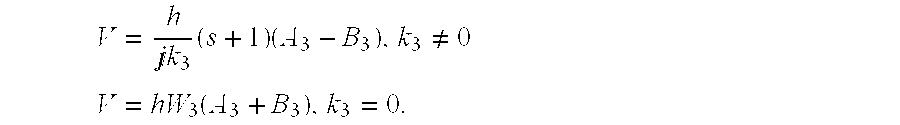
- ⁇ i ( x i ) A i e ⁇ jk i x i +B i e +jk i x i
- the strength of the resonance modes is determined by their piezoelectric coupling.
- the piezoelectrically generated voltage V is proportional to the displacement ⁇ of the vibration.
- the amplitude coefficients A i and B i are determined by the boundary conditions.
- a classical crystal oscillator 610 whose structure is symmetrical so that the leftmost region 1 and the rightmost region 3 are identical, and the vibration is trapped in the center region 2.
- the displacement ⁇ and its differential ⁇ (or, in this model, d ⁇ /dx) in the three regions are ⁇ Region 1 2 3 ⁇ A 1 ⁇ ⁇ K i ⁇ x i A 2 ⁇ ⁇ - j ⁇ ⁇ k 2 ⁇ x 2 - B 2 ⁇ ⁇ j ⁇ ⁇ k 2 ⁇ x 2 B 3 ⁇ ⁇ - K 3 ⁇ x 3 ⁇ ⁇ ⁇ x K 1 ⁇ A 1 ⁇ ⁇ K 1 ⁇ x 1 - j ⁇ ⁇ k 2 ⁇ A 2 ⁇ ⁇ - j ⁇ ⁇ k 2 ⁇ x 2 + j ⁇ ⁇ k 2 ⁇ B 2 ⁇ ⁇ j ⁇ ⁇ k 2 ⁇ x 2 - K 3 ⁇ B 3 ⁇ ⁇ - K 3 ⁇ x 3 ⁇ ⁇ ( 0 ) 0 A 2 + B 2 B 3 ⁇ ⁇ ( W ) ⁇ 0 A
- ⁇ 0 is the displacement at the interface between regions 1 and 2.
- the region 3 is in the center of the structure.
- the regions 2 and 4 are identical and they are adjacent to region 3.
- the leftmost region 1 and the rightmost region 5 are also identical, and region 1 is adjacent to region 2 and region 5 is adjacent to region 4.
- the regions numbered with 1, 2, 3, 4 and 5 refer to a symmetric resonator having (at least) these five regions in this order.
- the displacement ⁇ , in regions 2, 3 and 4 is
- ⁇ 1 A 1 e ⁇ jk 1 x 1 +B 1 e +jk 1 x 1 ,
- the strength of the symmetric solutions is determined by the difference A 3 ⁇ B 3 , which can be small or vanish altogether.
- the strength of the symmetric resonance modes can be computed numerically.
- the wave number k 2 needs to have a real value.
- the optimal width of the frame-like zone is not necessarily the same as above discussed for the regions 2 and 4, but it can be found, for example, experimentally.
- the laterally one-dimensional model discusses extensional wave modes, resonators operating in shear mode can be analyzed similarly.
- the material properties and cut-off frequency related to extensional wave modes are usually different from those related to shear modes, so proper thickness and width of a frame-like zone are typically different for shear and extensional wave modes.
- the strongest piezoelectrically excited mode in the center area of the resonator structure is piston mode.
- the spurious resonances occurring at frequencies near the piston operation frequency have often only a weak coupling. This effect enhances the electrical properties of a resonator according to the invention even further.
- the spurious resonances are seldom purely symmetric or antisymmetric, so that the results concerning the antisymmetric or symmetric solutions (resonance modes) usually cannot be directly applied in real resonator structures.
- a resonator according to the invention comprises at least two regions: the center area, which is in the piezoelectrically excitable area of the resonator, and a frame-like zone, which confines the center area.
- the center area corresponds to the region 3 of the laterally one-dimensional model described above
- the frame-like zone corresponds to the regions 2 and 4 of the laterally one-dimensional lateral model.
- a suitable thickness of the frame-like zone depends on the dispersion relation k( ⁇ ) in the frame-like zone and in the material which surrounds the frame-like zone.
- the dispersion relation k( ⁇ ) may have one of the two general forms depicted in FIG. 7, where the angular frequency ⁇ is schematically presented as a function of the wave number k.
- the horizontal axis on the right side of the vertical axis represents real values of the wave number k and on the left side of the vertical axis the wave number is imaginary.
- the vertical axis in FIG. 7 represents the angular frequency ⁇ .
- the wave number k is real, when the angular frequency ⁇ is above the cut-off angular frequency ⁇ c of the plate.
- the wave number k is real, when the angular frequency ⁇ is below the cut-off angular frequency ⁇ c .
- the dispersion of TE1 (first thickness extensional) mode is of the type I when the Poisson's ratio of the material is above 1 ⁇ 3 and of the type II when the ratio is below 1 ⁇ 3.
- the center area of a resonator according to the invention may operate in the piston mode under piezoelectric excitation, when at the operation frequency the wave number is real in the frame-like zone, zero in the center region and imaginary in the material surrounding the frame-like.
- the cut-off frequency has to be lower than the operating frequency, when the dispersion k( ⁇ ) is of type I. If the dispersion is of type I, then the cut-off frequency has to be higher than the operating frequency for the wave number to be real at the operating frequency.
- the operating frequency of piston mode is the same as the cut-off frequency of the center area of a resonator.
- the rule for choosing the angular cut-off frequencies ⁇ C1 in the surrounding area and ⁇ C2 in the frame-like zone is that the wave number in the surrounding area is imaginary and in the frame-like zone real at the piston mode frequency, which is the cut-off frequency ⁇ C3 in the center region.
- Table 1 summarizes suitable choices for the angular cut-off frequencies ⁇ C at the frame-like zone (region 2) and at the material surrounding the frame-like zone (region 1).
- the cut-off frequency can be adjusted, for example, by adjusting the thickness of the layers at these regions.
- the angular frequency ⁇ C3 denotes to the angular cut-off frequency of the center area of a resonator (region 3).
- Table 2 shows six examples of laterally one-dimensional resonator structures according to the invention.
- the six examples present possible combinations of the two dispersion types I and II in the regions 1 and 2.
- the wave numbers k 1 and k 2 are calculated using a dispersion relation
- FIGS. 8 a - 8 f present schematically partial cross-sections of the resonator structures specified in Table 2.
- the various cut-off frequencies of Table 2 are presented in FIG. 8 as a varying thickness of a resonator structure: usually the higher cut-off frequency means a thinner plate, and this is the logic in FIG. 8 . Please note, however, that in addition to the thickness of the layers, the material of the layers forming a plate also affects the cut-off frequency of the plate.
- FIG. 8 a presents a partial cross section of a resonator 810 , where both in region 1 and region 2 the dispersion is of type I.
- the relation of the cut-off frequencies in resonator 810 is the following: ⁇ C2 ⁇ C3 ⁇ C1 .
- the frame-like zone of a resonator according to the invention is thicker than the center area, and the region surrounding the frame-like zone is thinner than the frame-like zone.
- FIG. 8 b shows a resonator 820 , where the dispersion in region 1 is of type I and in region 2 the dispersion is of type II.
- the relation of the cut-off frequencies in resonator 820 is the following: ⁇ C3 ⁇ C2 ⁇ C1 . In this case, usually both the frame-like zone and the region surrounding the frame-like zone are thinner than the center area of a resonator.
- FIG. 8 c presents a resonator 830 , where the dispersion in region 1 is of type II and in region 2 it is of type I, and the relation of the cut-off frequencies is ⁇ C2 ⁇ C1 ⁇ C3 .
- the dispersion is of type II in both the regions 1 and 2 of resonator 840 , and the relation of the cut-off frequencies is ⁇ C1 ⁇ C3 ⁇ C2 .
- FIG. 8 e shows a partial cross section of a resonator 850 , where the dispersion is of type II in region 2 and of type I in region 1 and the relation of the cut-off frequencies is ⁇ C3 ⁇ C1 ⁇ C2 .
- 8 f shows a partial cross section of a resonator 860 , where the dispersion is of type I both in region 1 and 2.
- the relation of the cut-off frequencies is ⁇ C1 ⁇ C2 ⁇ C3 in resonator 860 .
- the calculated electrical responses of three laterally one-dimensional resonators having the structure specified in FIG. 8 a is presented in FIG. 9 .
- the width W 2 of the boundary region 2 varies from resonator to resonator, and the three widths W 2 are 6 ⁇ m, 12.93 ⁇ m and 18 ⁇ m.
- Smith's chart is a way to present the impedance of a certain electrical component as a function of the frequency.
- frequency increases in a clockwise manner.
- a resonator which resonates only in the basic resonance mode produces a circle on Smith's chart.
- Possible loops in the diagram indicate spurious resonance frequencies. The size of the loops indicates the strength of the spurious resonances.
- Table 3 presents a further example of a laterally one-dimensional resonator according to the invention.
- This resonator has a typical layer structure of a BAW resonator. It comprises a top electrode made of aluminium and a bottom electrode made of molybdenum. In between these electrodes, there is a piezoelectric layer of ZnO. The resonator structure is on a support layer made of SiO 2 . Table 3 specifies the widths of regions 1-5 and the thickness of each layer at the regions. In the BAW resonator described in Table 3 the frame-like zone is formed by making the top electrode thicker near its edges.
- the thickness and width of the frame-like zone (boundary region 2;4) in a resonator according to the invention may be estimated based on the following design rule.
- an infinitely long slab which has a width 2W 2 , whose the layer structure is that of the boundary region 2;4 and which is surrounded by both sides by the layer stack of region 1;5.
- the width 2W 2 is chosen so that the lowest lateral resonance frequency in the slab is equal to the cut-off frequency of the center area of the resonator.
- the width of the actual boundary region 2;4 in the complete resonator is then half of the width of the slab, in other words it is W 2 .
- the frequency of the lowest lateral resonance mode of a infinitely long slab whose width is 2W 2 , whose layer structure is known and where also the layer structure adjacent to the slab is known, can be determined straightforwardly, for example, using finite element method (FEM).
- FEM finite element method
- the cut-off frequency of a layer structure can be determined, when the materials and the thicknesses of the layers are known. This design rule produces practically the same width for the fame-like zone as the laterally one-dimensional model described above.
- material parameter values of Al, Mo, SiO 2 and ZnO found in the literature are used.
- FIG. 10 presents schematically the BAW resonator structure 1000 specified in Table 3.
- the SiO 2 support layer 200 corresponds to a substrate.
- the bottom electrode 110 and the ZnO piezoelectric layer 100 extend over the whole resonator width.
- the top electrode 120 covers the boundary regions 2 and 4, and the center region 3.
- the boundary regions 2 and 4 of the resonator structure 1000 are formed by making the top electrode 120 thicker at the edge of the electrically excitable area.
- the arrows in FIG. 10 indicate the scale; please note that the scale is different in the horizontal and vertical directions.
- FIG. 11 presents on Smith's chart the calculated electrical response of two resonator structures.
- the other is a resonator structure 1000 specified in Table 3 and presented in FIG. 10 . It is thus a resonator according to the invention, and its electrical response is illustrated with a solid line in FIG. 11 .
- the dashed line in FIG. 11 presents the electrical response of a resonator structure which does not comprise a boundary region according to the invention.
- This flat resonator is otherwise similar to that specified in Table 3, but the thickness of the top electrode at the regions 2 and 4 is 400 nm. In other words, the top electrode has uniform thickness.
- the center region can be obtained to operate in piston mode, and this does not depend on the width of the center region.
- the center area 3 of a real resonator having finite lateral dimensions does not have to have any specific form.
- the center area in a resonator according to the invention is thus not restricted to any specific forms, and it may have, for example, the free-shaped form illustrated in FIG. 12 a .
- the center area 3 may, for example, be rectangular as in resonator 1210 in FIG. 12 b , polygonal as in resonator 1220 in FIG. 12 c or circular as in resonator 1230 in FIG. 12 d.
- the shape of the electrically excitable area can be different from the shape of the center area, as long as the center area is within the electrically excitable area.
- the frame-like zone may be on the electrically excitable area, it may be partially on the electrically excitable area or it may encircle the electrically excitable. In the last case, the electrically excitable area is the same as the center area. Typically it is advantageous to restrict the electrically excitable area to the area confined by the outer circle of the frame-like zone.
- the laterally one-dimensional model above discusses only regions with constant thickness. It is also possible to construct resonators where the thickness varies within the regions.
- the width of the frame-like zone in real three-dimensional resonators can be estimated, for example, using the design rule presented above.
- the exact optimum dimensions for the frame-like zone are often found experimentally because, for example, of the uncertainties in the material parameters in thin films.
- the frame-like zone is constructed by making at least one of the layer thicker around the center area.
- the BAW resonator 1000 presented in FIG. 10 is an example of a resonator according to a first preferred embodiment of the invention; there the frame-like zone is formed by the thickness variation of the top electrode 120 . If the frame-like zone is formed by thickening the top electrode, then frame-like zone is typically within the electrically excitable area.
- FIG. 13 shows a BAW resonator 1300 according to a second preferred embodiment of the invention.
- the BAW resonator 1300 is fabricated on a glass or silicon substrate 200 . Over the substrate, there is, for example, a membrane layer 130 and an etch pit 210 isolating the resonator structure from the substrate.
- the bottom electrode 110 covers a certain part of the substrate, and it is covered by the piezoelectric layer 100 . Part of the bottom electrode 110 is left exposed for allowing the joining of the resonator to electrical components.
- the top electrode 120 covers at least part of the piezoelectric layer 100 .
- the frame-like boundary zone 2 is formed by depositing an extra frame-like layer 2 to the resonator structure.
- the same-like layer 2 according to the invention may be situated between any layers of a resonator structure.
- the extra layer is deposited on top of the top electrode 120 .
- the extra frame-like layer may be electrically conducting or isolating.
- An extra frame-like layer may, for example, encircle the electrically excitable area, being itself outside the electrically excitable area of a resonator, or it may be located at the edge of the electrically excitable area as in FIG. 13 .
- the edges of the piezoelectric layer 100 may be slanting.
- the patterning of the piezoelectric material typically produces edges that are not exactly perpendicular to the surface of the substrate.
- a resonator structure according to the invention may have such slanting edges and still operate successfully in piston mode. If the edges of the piezoelectric layer (or of any other layer, but typically the piezoelectric layer is the thickest layer in a resonator structure) are slanting already just beside the frame-like zone, the width of the frame-like zone may need adjustment when compared to the width calculated using either the laterally one-dimensional theory or the design rule described above because the acoustic properties of the surrounding region 1;5 are then changing.
- the top electrode 120 of the resonator 1300 extends as a strip to the right-hand side (in FIG. 13 ), covering part of the slanting edge of the piezoelectric layer.
- FIG. 14 shows schematically a BAW resonator 1400 according to a third preferred embodiment of the invention, where the frame-like boundary zone is formed by letting two layers overlap.
- the BAW resonator 1400 is by way of example on a membrane 130 placed over a etch pit 210 .
- the BAW resonator 1400 has a top electrode 120 and a bottom electrode 110 , and a piezoelectric layer 100 in between the electrodes.
- the piezoelectric layer 100 may be covered with a passivation layer 140 .
- the passivation layer is typically dielectric material, and it both insulates the component electrically and protects the piezoelectric material.
- the passivation layer is opened (or removed by etching) on top of the piezoelectric layer 100 , on the location where the top electrode 120 is placed. As can be seen in FIG. 14, the passivation layer 140 and the top electrode 120 overlap at the edge of the top electrode.
- the zone, where both the top electrode 120 and the passivation layer 140 extend, is the frame-like zone according to the invention. It is also possible that the layers which overlap and form the frame-like zone, are not the top-most layers of the resonator structure.
- FIG. 15 the measured electrical response of a BAW resonator according to the third preferred embodiment of the invention is compared to the electrical response of flat prior-art BAW resonator.
- Both these BAW resonators employ an acoustic quarter-wavelength mirror layer.
- the piezoelectric material is ZnO, which exhibits dispersion relation of type I for TE1 waves.
- the BAW resonator X10#46 D76M124 according to a third preferred embodiment has a frame-like zone that is 235 nm thicker than the center area of the resonator and that is 5 ⁇ m wide which has been experimentally found to be optimum for the studied resonator X10#46 D76M124.
- the frame-like zone is constructed by letting a passivation layer and the top electrode overlap at the edge of the top electrode.
- the BAW resonator X10#46 D77T8 is a flat prior-art BAW resonator. It has otherwise similar layer structure and dimensions as the BAW resonator X10#46 D76M124, but it lacks the frame-like zone.
- the measured electrical response of the BAW resonator X10#46 D76M124 is presented in FIG. 15 with a dashed line.
- the dashed line does not deviate much from a circle, indicating that the BAW resonator X10#46 D76M124 according to the third preferred embodiment of the invention operates in the piston mode.
- the measured electrical response of the BAW resonator X10#46 D77T8 is presented in FIG. 15 with a solid line.
- the solid line forms loops, indicating that the prior-art BAW resonator without a frame-like zone has spurious resonances.
- FIG. 16 shows the measured electrical responses of various BAW resonators, and it gives an example of selecting the width of the frame-like zone properly.
- these BAW resonators a SiO 2 passivation layer overlaps with the top electrode, similarly as presented in FIG. 14, forming a frame-like zone.
- the width of the frame-like zone is different in each BAW resonator, whose electrical response is presented in FIG. 16 .
- the width varies from 1 ⁇ m to 9 ⁇ m from resonator to resonator, but it is practically uniform for each resonator.
- FIG. 16 presents the purity of the electrical response as deviation from a circle on Smith's chart as a function of frequency.
- the amplitude of the waves indicates the strength of the spurious resonances.
- the curves in FIG. 16 correspond to the following widths of the frame-like zone: 1, 3, 5, 7 and 9 ⁇ m.
- the curves marked with 7, 5, 3 and 1 ⁇ m have been shifted in the vertical direction by ⁇ 0.1, ⁇ 0.2, ⁇ 0.3 and ⁇ 0.4, correspondingly, to enhance legibility.
- the BAW resonator having a 7- ⁇ m wide frame-like zone has the purest electrical response in FIG. 16, and it is a resonator according to the invention.
- the deviations from the circle on Smith's chart are less than 0.02 units.
- the width of the frame-like zone is smaller, the deviation from the circle increases.
- the resonator having a 1 ⁇ m wide frame-like zone exhibits at least 14 spurious resonance modes at the frequency range of 820 . . . 870 MHz.
- FIG. 16 (curve marked with 9 ⁇ m) shows that spurious resonances emerge at somewhat lower frequencies.
- FIG. 17 shows a cross-section of a resonator structures 1700 and 1710 according to a fourth preferred embodiment of the invention.
- a resonator according to the invention may have a frame-like zone, whose cross-section is not rectangular.
- the edges of any layer in the layer structure may be tapered. Usually the edges of the frame-like zone become automatically tapered when wet etching technique is used.
- Resonator structure 1700 is given as an example. The correct dimensions for the edge regions are found numerically, by solving the wave equation, or experimentally by observing the strength of the spurious modes.
- the edge of the piezoelectric layer 100 may be thinned gradually, as shown in FIG. 17 b for the resonator 1710 . Due to the tapering of the piezoelectric layer, the cut-off frequency of the frame-like zone varies smoothly as a function of the distance from the center of the resonator.
- a BAW resonator according to the fourth preferred embodiment of the invention may be quite simple to produce, as many thin film patterning procedures produce tapered edges in proper dimension. The width of the sloping edge of a film typically becomes comparable to the thickness of the film.
- FIG. 18 shows a top-view of some example resonator structures according to a fifth preferred embodiment of the invention.
- the frame-like zone is formed by patterning one of the layers in the layer structure.
- the patterned layer may be, for example, the top electrode 120 , as presented in FIG. 18 a
- the resonator 1810 has a frame-like zone 2 , which is formed by patterning the rim of the top electrode 120 in a suitable way. If the dimensions of the patterning image are small compared to the wavelength of the sound in the lateral direction, the cut-off frequency of the patterned region, which is indicated with dashed lines in FIGS. 18 a and 18 b , is changed.
- Patterning can be used to fabricate a frame-like zone having a higher (FIG. 18 a ) or lower (FIG. 18 c ) cut-off frequency than the center area without deposition of a new layer.
- the patterned layer may be one of the layers extending over the center area of the resonator, for example to top electrode, or it may be one of the layers extending over the region surrounding the center area.
- the manufacture of a resonator having a patterned frame-like zone typically does not require extra steps compared to manufacture of prior-art resonators. It is also possible to deposit a separate layer which forms only the patterning, but does not extend neither to the center area nor to the region surrounding the center area. Furthermore, it is possible to vary the thickness of a layer so that a patterning image specifies the thickness of a layer instead of specifying the absence/presence of a layer.
- Typical dimensions of the patterning image can thus be, for example, several micrometers. The dimensions may also be less, if such dimensions are technically feasible to achieve.
- FIGS. 18 c and 18 d show top views of two examples of patterning, which can be used to form a frame-like zone.
- Figures presenting resonator structures according to the invention present, as examples, resonators having one piezoelectric layer.
- a resonator according to the invention may as well have, for example, two piezoelectric layers and a middle electrode, or it may have more than one middle electrodes stacked in between piezoelectric layers.
- Bulk acoustic wave resonators are used above as examples of piezoelectric resonators, where a frame-like zone enhances the properties of a resonator.
- a frame-like zone according to the invention may be used to enhance the properties of thicker crystal resonators, too.
- Suitable cut-off frequency relating to the piezoelectrically excited wave mode in the frame-like zone and width of the frame-like zone may be found using the principles presented above.
- the width of the frame-like zone refers to dimension of the frame-like zone in the direction of the surface of the top electrode. Any expressions indicating directions, such as top and bottom, are used to make the description of the resonator structure more eligible. These expressions do not restrict the resonator structures according to the invention in any way.
Landscapes
- Physics & Mathematics (AREA)
- Acoustics & Sound (AREA)
- Piezo-Electric Or Mechanical Vibrators, Or Delay Or Filter Circuits (AREA)
Abstract
Description


| TABLE 1 |
| The design rules for achieving piston mode operation. |
| Region of resonator structure | Dispersion type | Design rule | ||
| Region 1 | I | ωC1 > ωC3 | ||
| Region 1 | II | ωC1 < ωC3 | ||
| Region 2 | I | ωC2 < ωC3 | ||
| Region 2 | II | ωC2 > ωC3 | ||
| TABLE 2 |
| Some resonator structures that produce piston mode operation. |
| Partial cross-section in Figure |
| 8a | 8b | 8c | 8d | 8e | 8f | |||
| Dispersion in | I | I | II | II | | II | |
| region | |||||||
| 1 | |||||||
| Dispersion in | I | II | I | II | II | I | |
| |
|||||||
| Dispersion in | I | I | I | I | | I | |
| region | |||||||
| 3 | |||||||
| α in |
10−8 | 10−8 | −10−8 | −10−8 | 10−8 | −10−8 | s2/m2 rad2 |
| α in |
10−8 | −10−8 | 10−8 | −10−8 | −10−8 | 10−8 | s2/m2 rad2 |
| α in |
10−8 | 10−8 | 10−8 | 10−8 | 10−8 | 10−8 | s2/m2 rad2 |
| ωc,1 | 6.05 | 6.05 | 5.95 | 5.95 | 6.03 | 5.93 | 109 rad/s |
| ωc,2 | 5.93 | 6.03 | 5.93 | 6.03 | 6.05 | 5.95 | 109 rad/s |
| ωc,3 | 6.00 | 6.00 | 6.00 | 6.00 | 6.00 | 6.00 | 109 rad/s |
| k1 | j77621 | j77621 | j77298 | j77298 | j60075 | j91384 | l/m |
| k2 | 91384 | 60075 | 91384 | 60075 | 77621 | 77298 | l/m |
| k3 | 0 | 0 | 0 | 0 | 0 | 0 | l/m |
| W2 (n = 0) | 7.7 | 15.2 | 7.7 | 15.2 | 8.5 | 11.2 | μm |
| W2 (n = 1) | 42.1 | 67.5 | 42.1 | 67.4 | 49.0 | 51.9 | μm |
| TABLE 3 |
| Structure of an example BAW resonator according to the invention. |
| |
1 | 2 | 3 | 4 | 5 |
| Top electrode A1 (nm) | 0 | 500 | 400 | 500 | 0 |
| Piezoelectric layer ZnO | 2200 | 2200 | 2200 | 2200 | 2200 |
| (nm) | |||||
| Bottom electrode Mo | 400 | 400 | 400 | 400 | 400 |
| (nm) | |||||
| Support layer SiO2 (nm) | 500 | 500 | 500 | 500 | 500 |
| Width of region (μm) | 40 | 4.29 | 250 | 4.29 | 40 |
| Cut-off freq.fc (MHz) | 1059.94 | 973.48 | 990.90 | 973.48 | 1059.94 |
| Electrodes | No | Yes | Yes | Yes | No |
| |
1000 | 1000 | 1000 | 1000 | 1000 |
Claims (39)
Applications Claiming Priority (3)
| Application Number | Priority Date | Filing Date | Title |
|---|---|---|---|
| FI991619A FI107660B (en) | 1999-07-19 | 1999-07-19 | resonator |
| FI991619 | 1999-07-19 | ||
| PCT/FI2000/000591 WO2001006647A1 (en) | 1999-07-19 | 2000-06-29 | Resonator structure and a filter comprising such a resonator structure |
Publications (1)
| Publication Number | Publication Date |
|---|---|
| US6812619B1 true US6812619B1 (en) | 2004-11-02 |
Family
ID=8555088
Family Applications (2)
| Application Number | Title | Priority Date | Filing Date |
|---|---|---|---|
| US10/031,579 Expired - Lifetime US6812619B1 (en) | 1999-07-19 | 2000-06-29 | Resonator structure and a filter comprising such a resonator structure |
| US10/031,533 Expired - Lifetime US6788170B1 (en) | 1999-07-19 | 2000-07-18 | Resonator structure having a dampening material and a filter having such a resonator structure |
Family Applications After (1)
| Application Number | Title | Priority Date | Filing Date |
|---|---|---|---|
| US10/031,533 Expired - Lifetime US6788170B1 (en) | 1999-07-19 | 2000-07-18 | Resonator structure having a dampening material and a filter having such a resonator structure |
Country Status (8)
| Country | Link |
|---|---|
| US (2) | US6812619B1 (en) |
| EP (3) | EP2782250A1 (en) |
| JP (2) | JP3735777B2 (en) |
| CN (2) | CN1183669C (en) |
| AU (2) | AU5687800A (en) |
| DE (1) | DE60042486D1 (en) |
| FI (1) | FI107660B (en) |
| WO (2) | WO2001006647A1 (en) |
Cited By (157)
| Publication number | Priority date | Publication date | Assignee | Title |
|---|---|---|---|---|
| US20040140869A1 (en) * | 2002-11-07 | 2004-07-22 | Stephan Marksteiner | Acoustic reflector for a BAW resonator |
| US20040163244A1 (en) * | 2000-10-30 | 2004-08-26 | Agere Systems Inc. | Method of manufacturing and mounting electronic devices to limit the effects of parasitics |
| US20050140465A1 (en) * | 2003-12-30 | 2005-06-30 | Keh-Long Hwu | Noise suppression method for wave filter |
| US20050275486A1 (en) * | 2004-06-14 | 2005-12-15 | Hongiun Feng | Acoustic resonator performance enhancements using recessed region |
| US20060071736A1 (en) * | 2004-10-01 | 2006-04-06 | Ruby Richard C | Acoustic resonator performance enhancement using alternating frame structure |
| US20060128058A1 (en) * | 2004-12-15 | 2006-06-15 | Dungan Thomas E | Wafer bonding of micro-electro mechanical systems to active circuitry |
| US20070210878A1 (en) * | 2006-03-08 | 2007-09-13 | Ngk Insulators, Ltd. | Piezoelectric thin film device |
| US20070278899A1 (en) * | 2005-02-21 | 2007-12-06 | Murata Manufacturing Co., Ltd. | Piezoelectric thin-film resonator |
| US7332985B2 (en) | 2003-10-30 | 2008-02-19 | Avago Technologies Wireless Ip (Singapore) Pte Ltd. | Cavity-less film bulk acoustic resonator (FBAR) devices |
| EP1890380A1 (en) | 2006-08-16 | 2008-02-20 | Samsung Electronics Co., Ltd. | Resonator and fabrication method thereof |
| US7362198B2 (en) | 2003-10-30 | 2008-04-22 | Avago Technologies Wireless Ip (Singapore) Pte. Ltd | Pass bandwidth control in decoupled stacked bulk acoustic resonator devices |
| US20080094154A1 (en) * | 2006-08-01 | 2008-04-24 | Epcos Ag | Bulk acoustic wave resonator and filter |
| US7369013B2 (en) | 2005-04-06 | 2008-05-06 | Avago Technologies Wireless Ip Pte Ltd | Acoustic resonator performance enhancement using filled recessed region |
| US7367095B2 (en) | 2003-10-30 | 2008-05-06 | Avago Technologies General Ip Pte Ltd | Method of making an acoustically coupled transformer |
| US7388455B2 (en) | 2003-10-30 | 2008-06-17 | Avago Technologies Wireless Ip Pte Ltd | Film acoustically-coupled transformer with increased common mode rejection |
| US7391286B2 (en) | 2005-10-06 | 2008-06-24 | Avago Wireless Ip Pte Ltd | Impedance matching and parasitic capacitor resonance of FBAR resonators and coupled filters |
| US20080174389A1 (en) * | 2005-06-02 | 2008-07-24 | Yuka Mori | Piezoelectric Resonator and Piezoelectric Thin-Film Filter |
| US20080179995A1 (en) * | 2005-11-04 | 2008-07-31 | Murata Manufacturing Co., Ltd. | Piezoelectric thin-film resonator |
| US7423503B2 (en) | 2005-10-18 | 2008-09-09 | Avago Technologies Wireless Ip (Singapore) Pte. Ltd. | Acoustic galvanic isolator incorporating film acoustically-coupled transformer |
| US7424772B2 (en) | 2003-10-30 | 2008-09-16 | Avago Technologies Wireless Ip (Singapore) Pte. Ltd. | Stacked bulk acoustic resonator band-pass filter with controllable pass bandwidth |
| US7425787B2 (en) | 2005-10-18 | 2008-09-16 | Avago Technologies Wireless Ip (Singapore) Pte. Ltd. | Acoustic galvanic isolator incorporating single insulated decoupled stacked bulk acoustic resonator with acoustically-resonant electrical insulator |
| US7427819B2 (en) | 2005-03-04 | 2008-09-23 | Avago Wireless Ip Pte Ltd | Film-bulk acoustic wave resonator with motion plate and method |
| US7436269B2 (en) | 2005-04-18 | 2008-10-14 | Avago Technologies Wireless Ip (Singapore) Pte. Ltd. | Acoustically coupled resonators and method of making the same |
| US7463499B2 (en) | 2005-10-31 | 2008-12-09 | Avago Technologies General Ip (Singapore) Pte Ltd. | AC-DC power converter |
| US7479685B2 (en) | 2006-03-10 | 2009-01-20 | Avago Technologies General Ip (Singapore) Pte. Ltd. | Electronic device on substrate with cavity and mitigated parasitic leakage path |
| US20090033177A1 (en) * | 2005-08-08 | 2009-02-05 | Kabushiki Kaisha Toshiba | Thin film piezoelectric resonator and method of manufacturing the same |
| US20090045704A1 (en) * | 2007-08-14 | 2009-02-19 | Skyworks Solutions, Inc. | Method for forming a multi-layer electrode underlying a piezoelectric layer and related structure |
| US20090045703A1 (en) * | 2007-08-14 | 2009-02-19 | Skyworks Solutions, Inc. | Bulk acoustic wave structure with aluminum cooper nitride piezoelectric layer and related method |
| US7508286B2 (en) | 2006-09-28 | 2009-03-24 | Avago Technologies Wireless Ip (Singapore) Pte. Ltd. | HBAR oscillator and method of manufacture |
| US7525398B2 (en) | 2005-10-18 | 2009-04-28 | Avago Technologies General Ip (Singapore) Pte. Ltd. | Acoustically communicating data signals across an electrical isolation barrier |
| US7557677B1 (en) * | 2006-12-20 | 2009-07-07 | Hrl Laboratories, Llc | Cascaded monolithic crystal filter with high out-of-band rejection |
| US7561009B2 (en) | 2005-11-30 | 2009-07-14 | Avago Technologies General Ip (Singapore) Pte. Ltd. | Film bulk acoustic resonator (FBAR) devices with temperature compensation |
| US20090206706A1 (en) * | 2008-02-20 | 2009-08-20 | Fujitsu Limited | Piezoelectric thin-film resonator |
| US7602102B1 (en) | 2008-04-24 | 2009-10-13 | Skyworks Solutions, Inc. | Bulk acoustic wave resonator with controlled thickness region having controlled electromechanical coupling |
| US20090267457A1 (en) * | 2008-04-24 | 2009-10-29 | Skyworks Solutions, Inc. | Bulk acoustic wave resonator with reduced energy loss |
| US7612636B2 (en) | 2006-01-30 | 2009-11-03 | Avago Technologies Wireless Ip (Singapore) Pte. Ltd. | Impedance transforming bulk acoustic wave baluns |
| US7615833B2 (en) | 2004-07-13 | 2009-11-10 | Avago Technologies Wireless Ip (Singapore) Pte. Ltd. | Film bulk acoustic resonator package and method of fabricating same |
| US7629865B2 (en) | 2006-05-31 | 2009-12-08 | Avago Technologies Wireless Ip (Singapore) Pte. Ltd. | Piezoelectric resonator structures and electrical filters |
| US7675390B2 (en) | 2005-10-18 | 2010-03-09 | Avago Technologies Wireless Ip (Singapore) Pte. Ltd. | Acoustic galvanic isolator incorporating single decoupled stacked bulk acoustic resonator |
| US20100107400A1 (en) * | 2006-05-17 | 2010-05-06 | Avago Technologies Wireless Ip (Singapore) Pte.Ltd | Method of manufacturing an acoustic mirror |
| US20100134210A1 (en) * | 2007-07-20 | 2010-06-03 | Murata Manufacturing Co., Ltd. | Piezoelectric Resonator and Piezoelectric Filter Device |
| US7732977B2 (en) | 2008-04-30 | 2010-06-08 | Avago Technologies Wireless Ip (Singapore) | Transceiver circuit for film bulk acoustic resonator (FBAR) transducers |
| US20100141353A1 (en) * | 2007-08-24 | 2010-06-10 | Fujitsu Limited | Piezoelectric thin film resonator, filter using the resonator, duplexer using the filter, and communication equipment using the filter or the duplexer |
| US7737807B2 (en) | 2005-10-18 | 2010-06-15 | Avago Technologies Wireless Ip (Singapore) Pte. Ltd. | Acoustic galvanic isolator incorporating series-connected decoupled stacked bulk acoustic resonators |
| US7746677B2 (en) | 2006-03-09 | 2010-06-29 | Avago Technologies Wireless Ip (Singapore) Pte. Ltd. | AC-DC converter circuit and power supply |
| US20100163410A1 (en) * | 2008-12-30 | 2010-07-01 | Stmicroeletronics S.R.I. | Electronic detection of biological materials |
| US7791434B2 (en) | 2004-12-22 | 2010-09-07 | Avago Technologies Wireless Ip (Singapore) Pte. Ltd. | Acoustic resonator performance enhancement using selective metal etch and having a trench in the piezoelectric |
| US7791435B2 (en) | 2007-09-28 | 2010-09-07 | Avago Technologies Wireless Ip (Singapore) Pte. Ltd. | Single stack coupled resonators having differential output |
| US20100231329A1 (en) * | 2007-10-18 | 2010-09-16 | Barber Bradley P | Baw structure with reduced topographic steps and related method |
| US7802349B2 (en) | 2003-03-07 | 2010-09-28 | Avago Technologies Wireless Ip (Singapore) Pte. Ltd. | Manufacturing process for thin film bulk acoustic resonator (FBAR) filters |
| US7855618B2 (en) | 2008-04-30 | 2010-12-21 | Avago Technologies Wireless Ip (Singapore) Pte. Ltd. | Bulk acoustic resonator electrical impedance transformers |
| US7868522B2 (en) | 2005-09-09 | 2011-01-11 | Avago Technologies Wireless Ip (Singapore) Pte. Ltd. | Adjusted frequency temperature coefficient resonator |
| US20110037539A1 (en) * | 2008-04-29 | 2011-02-17 | Nxp B.V. | Bulk acoustic wave resonator |
| US20110233922A1 (en) * | 2006-05-05 | 2011-09-29 | Weems Industries, Inc. | Identification system for pneumatic couplers |
| US8193877B2 (en) | 2009-11-30 | 2012-06-05 | Avago Technologies Wireless Ip (Singapore) Pte. Ltd. | Duplexer with negative phase shifting circuit |
| US8222795B2 (en) | 2009-01-26 | 2012-07-17 | Resonance Semiconductor Corporation | Protected resonator |
| US20120182090A1 (en) * | 2011-01-19 | 2012-07-19 | Wei Pang | Acoustic wave resonator |
| US8248185B2 (en) | 2009-06-24 | 2012-08-21 | Avago Technologies Wireless Ip (Singapore) Pte. Ltd. | Acoustic resonator structure comprising a bridge |
| US20120248941A1 (en) * | 2011-03-29 | 2012-10-04 | Avago Technologies Wireless Ip (Singapore) Pte. Lt | Stacked bulk accoustic resonator and method of fabricating the same |
| US8350445B1 (en) | 2011-06-16 | 2013-01-08 | Avago Technologies Wireless Ip (Singapore) Pte. Ltd. | Bulk acoustic resonator comprising non-piezoelectric layer and bridge |
| US8749320B2 (en) | 2009-08-17 | 2014-06-10 | Taiyo Yuden Co., Ltd. | Acoustic wave device and method for manufacturing the same |
| US8796904B2 (en) | 2011-10-31 | 2014-08-05 | Avago Technologies General Ip (Singapore) Pte. Ltd. | Bulk acoustic resonator comprising piezoelectric layer and inverse piezoelectric layer |
| US8816567B2 (en) | 2011-07-19 | 2014-08-26 | Qualcomm Mems Technologies, Inc. | Piezoelectric laterally vibrating resonator structure geometries for spurious frequency suppression |
| US20140292152A1 (en) * | 2013-04-01 | 2014-10-02 | Cymatics Laboratories Corp. | Temperature compensating electrodes |
| US8854156B2 (en) | 2009-02-20 | 2014-10-07 | Ube Industries, Ltd. | Thin-film piezoelectric resonator and thin-film piezoelectric filter using the same |
| US8902023B2 (en) | 2009-06-24 | 2014-12-02 | Avago Technologies General Ip (Singapore) Pte. Ltd. | Acoustic resonator structure having an electrode with a cantilevered portion |
| US8922302B2 (en) | 2011-08-24 | 2014-12-30 | Avago Technologies General Ip (Singapore) Pte. Ltd. | Acoustic resonator formed on a pedestal |
| US8962443B2 (en) | 2011-01-31 | 2015-02-24 | Avago Technologies General Ip (Singapore) Pte. Ltd. | Semiconductor device having an airbridge and method of fabricating the same |
| US8981876B2 (en) | 2004-11-15 | 2015-03-17 | Avago Technologies General Ip (Singapore) Pte. Ltd. | Piezoelectric resonator structures and electrical filters having frame elements |
| US9048812B2 (en) | 2011-02-28 | 2015-06-02 | Avago Technologies General Ip (Singapore) Pte. Ltd. | Bulk acoustic wave resonator comprising bridge formed within piezoelectric layer |
| US9083302B2 (en) | 2011-02-28 | 2015-07-14 | Avago Technologies General Ip (Singapore) Pte. Ltd. | Stacked bulk acoustic resonator comprising a bridge and an acoustic reflector along a perimeter of the resonator |
| US9136818B2 (en) | 2011-02-28 | 2015-09-15 | Avago Technologies General Ip (Singapore) Pte. Ltd. | Stacked acoustic resonator comprising a bridge |
| US9148117B2 (en) | 2011-02-28 | 2015-09-29 | Avago Technologies General Ip (Singapore) Pte. Ltd. | Coupled resonator filter comprising a bridge and frame elements |
| US9154112B2 (en) | 2011-02-28 | 2015-10-06 | Avago Technologies General Ip (Singapore) Pte. Ltd. | Coupled resonator filter comprising a bridge |
| US9166552B2 (en) | 2011-05-24 | 2015-10-20 | Taiyo Yuden Co., Ltd. | Filter and duplexer |
| US9203374B2 (en) | 2011-02-28 | 2015-12-01 | Avago Technologies General Ip (Singapore) Pte. Ltd. | Film bulk acoustic resonator comprising a bridge |
| US9243316B2 (en) | 2010-01-22 | 2016-01-26 | Avago Technologies General Ip (Singapore) Pte. Ltd. | Method of fabricating piezoelectric material with selected c-axis orientation |
| JP2016504880A (en) * | 2013-01-11 | 2016-02-12 | ゼットティーイー コーポレーションZte Corporation | Low insertion loss piezoelectric acoustic bandpass filter and method of realization |
| US9362887B2 (en) | 2014-06-06 | 2016-06-07 | Akoustis, Inc. | Integrated circuit configured with two or more single crystal acoustic resonator devices |
| US9425764B2 (en) | 2012-10-25 | 2016-08-23 | Avago Technologies General Ip (Singapore) Pte. Ltd. | Accoustic resonator having composite electrodes with integrated lateral features |
| US9444426B2 (en) | 2012-10-25 | 2016-09-13 | Avago Technologies General Ip (Singapore) Pte. Ltd. | Accoustic resonator having integrated lateral feature and temperature compensation feature |
| US9450565B2 (en) | 2013-03-12 | 2016-09-20 | Qorvo Us, Inc. | Border ring mode suppression in solidly-mounted bulk acoustic wave resonator |
| US9537465B1 (en) | 2014-06-06 | 2017-01-03 | Akoustis, Inc. | Acoustic resonator device with single crystal piezo material and capacitor on a bulk substrate |
| US9608589B2 (en) | 2010-10-26 | 2017-03-28 | Avago Technologies General Ip (Singapore) Pte. Ltd. | Method of forming acoustic resonator using intervening seed layer |
| US9673384B2 (en) | 2014-06-06 | 2017-06-06 | Akoustis, Inc. | Resonance circuit with a single crystal capacitor dielectric material |
| US9716581B2 (en) | 2014-07-31 | 2017-07-25 | Akoustis, Inc. | Mobile communication device configured with a single crystal piezo resonator structure |
| US9735338B2 (en) | 2009-01-26 | 2017-08-15 | Cymatics Laboratories Corp. | Protected resonator |
| DE102016103959A1 (en) | 2016-03-04 | 2017-09-07 | Snaptrack, Inc. | BAW resonator with reduced spurious modes, BAW filter and method of manufacture |
| US9805966B2 (en) | 2014-07-25 | 2017-10-31 | Akoustis, Inc. | Wafer scale packaging |
| DE102016111061A1 (en) | 2016-06-16 | 2017-12-21 | Snaptrack, Inc. | Acoustic volume wave resonator with reduced losses, RF filter with such resonators and method for producing such resonators |
| US9912314B2 (en) | 2014-07-25 | 2018-03-06 | Akoustics, Inc. | Single crystal acoustic resonator and bulk acoustic wave filter |
| US9917568B2 (en) | 2014-08-26 | 2018-03-13 | Akoustis, Inc. | Membrane substrate structure for single crystal acoustic resonator device |
| US9985194B1 (en) | 2015-05-13 | 2018-05-29 | Qorvo Us, Inc. | Spurious mode suppression in bulk acoustic wave resonator |
| US9998094B2 (en) | 2014-12-05 | 2018-06-12 | Samsung Electro-Mechanics Co., Ltd. | Bulk acoustic wave resonator having a frame spaced apart from an electrode |
| US10110189B2 (en) | 2016-11-02 | 2018-10-23 | Akoustis, Inc. | Structure and method of manufacture for acoustic resonator or filter devices using improved fabrication conditions and perimeter structure modifications |
| US10177732B2 (en) | 2015-07-29 | 2019-01-08 | Taiyo Yuden Co., Ltd. | Piezoelectric thin film resonator, filter, and duplexer |
| WO2019029912A1 (en) * | 2017-08-07 | 2019-02-14 | RF360 Europe GmbH | Baw resonator with reduced spurious modes and increased quality factor |
| US10217930B1 (en) | 2016-03-11 | 2019-02-26 | Akoustis, Inc. | Method of manufacture for single crystal acoustic resonator devices using micro-vias |
| US10277194B2 (en) | 2017-09-15 | 2019-04-30 | Globalfoundries Singapore Pte. Ltd. | Acoustic MEMs resonator and filter with fractal electrode and method for producing the same |
| US10355659B2 (en) | 2016-03-11 | 2019-07-16 | Akoustis, Inc. | Piezoelectric acoustic resonator manufactured with piezoelectric thin film transfer process |
| US10355195B2 (en) | 2016-05-18 | 2019-07-16 | Samsung Electro-Mechanics Co., Ltd. | Acoustic resonator and method of manufacturing the same |
| US10431580B1 (en) | 2017-01-12 | 2019-10-01 | Akoustis, Inc. | Monolithic single chip integrated radio frequency front end module configured with single crystal acoustic filter devices |
| US10523180B2 (en) | 2016-03-11 | 2019-12-31 | Akoustis, Inc. | Method and structure for single crystal acoustic resonator devices using thermal recrystallization |
| US10581398B2 (en) | 2016-03-11 | 2020-03-03 | Akoustis, Inc. | Method of manufacture for single crystal acoustic resonator devices using micro-vias |
| US10615773B2 (en) | 2017-09-11 | 2020-04-07 | Akoustis, Inc. | Wireless communication infrastructure system configured with a single crystal piezo resonator and filter structure |
| US10637430B2 (en) | 2016-07-07 | 2020-04-28 | Samsung Electro-Mechanics Co., Ltd. | Bulk acoustic wave filter device and method of manufacturing the same |
| US10673513B2 (en) | 2016-03-11 | 2020-06-02 | Akoustis, Inc. | Front end module for 5.2 GHz Wi-Fi acoustic wave resonator RF filter circuit |
| US10680576B2 (en) | 2016-02-05 | 2020-06-09 | Taiyo Yuden Co., Ltd. | Piezoelectric thin film resonator, filter, and duplexer |
| US10790799B2 (en) | 2017-04-07 | 2020-09-29 | Taiyo Yuden Co., Ltd. | Piezoelectric thin film resonator, filter, and multiplexer |
| US10812040B2 (en) | 2018-07-24 | 2020-10-20 | Samsung Electro-Mechanics Co., Ltd. | Acoustic wave filter device |
| US10873316B2 (en) | 2017-03-02 | 2020-12-22 | Samsung Electro-Mechanics Co., Ltd. | Acoustic resonator and method of manufacturing the same |
| US10979022B2 (en) | 2016-03-11 | 2021-04-13 | Akoustis, Inc. | 5.2 GHz Wi-Fi acoustic wave resonator RF filter circuit |
| US10979023B2 (en) | 2016-03-11 | 2021-04-13 | Akoustis, Inc. | 5.9 GHz c-V2X and DSRC acoustic wave resonator RF filter circuit |
| US10979025B2 (en) | 2016-03-11 | 2021-04-13 | Akoustis, Inc. | 5G band n79 acoustic wave resonator RF filter circuit |
| US10979024B2 (en) | 2016-03-11 | 2021-04-13 | Akoustis, Inc. | 5.2 GHz Wi-Fi coexistence acoustic wave resonator RF filter circuit |
| US10979026B2 (en) | 2016-03-11 | 2021-04-13 | Akoustis, Inc. | 5.5 GHz Wi-fi 5G coexistence acoustic wave resonator RF filter circuit |
| US10985732B2 (en) | 2016-03-11 | 2021-04-20 | Akoustis, Inc. | 5.6 GHz Wi-Fi acoustic wave resonator RF filter circuit |
| US11063576B2 (en) | 2016-03-11 | 2021-07-13 | Akoustis, Inc. | Front end module for 5.6 GHz Wi-Fi acoustic wave resonator RF filter circuit |
| US11070184B2 (en) | 2016-03-11 | 2021-07-20 | Akoustis, Inc. | Piezoelectric acoustic resonator manufactured with piezoelectric thin film transfer process |
| US11082023B2 (en) * | 2018-09-24 | 2021-08-03 | Skyworks Global Pte. Ltd. | Multi-layer raised frame in bulk acoustic wave device |
| US11177868B2 (en) | 2016-03-11 | 2021-11-16 | Akoustis, Inc. | Front end module for 6.5 GHz Wi-Fi acoustic wave resonator RF filter circuit |
| US11184079B2 (en) | 2016-03-11 | 2021-11-23 | Akoustis, Inc. | Front end module for 5.5 GHz Wi-Fi acoustic wave resonator RF filter circuit |
| US11228299B2 (en) | 2017-02-02 | 2022-01-18 | Taiyo Yuden Co., Ltd. | Piezoelectric thin film resonator with insertion film, filter, and multiplexer |
| US11233496B2 (en) | 2018-02-21 | 2022-01-25 | Vanguard International Semiconductor Singapore Pte. Ltd. | Acoustic resonator and filter with electrode having zig-zag edge and method for producing the same |
| US11264970B2 (en) * | 2019-03-02 | 2022-03-01 | Texas Instruments Incorporated | Piezoelectric resonator with patterned resonant confiners |
| US11316496B2 (en) | 2016-03-11 | 2022-04-26 | Akoustis, Inc. | Method and structure for high performance resonance circuit with single crystal piezoelectric capacitor dielectric material |
| US11356071B2 (en) | 2016-03-11 | 2022-06-07 | Akoustis, Inc. | Piezoelectric acoustic resonator with improved TCF manufactured with piezoelectric thin film transfer process |
| US11394451B2 (en) | 2016-03-11 | 2022-07-19 | Akoustis, Inc. | Front end module for 6.1 GHz Wi-Fi acoustic wave resonator RF filter circuit |
| US11411168B2 (en) | 2017-10-16 | 2022-08-09 | Akoustis, Inc. | Methods of forming group III piezoelectric thin films via sputtering |
| US11411169B2 (en) | 2017-10-16 | 2022-08-09 | Akoustis, Inc. | Methods of forming group III piezoelectric thin films via removal of portions of first sputtered material |
| US11418169B2 (en) | 2016-03-11 | 2022-08-16 | Akoustis, Inc. | 5G n41 2.6 GHz band acoustic wave resonator RF filter circuit |
| US11424728B2 (en) | 2016-03-11 | 2022-08-23 | Akoustis, Inc. | Piezoelectric acoustic resonator manufactured with piezoelectric thin film transfer process |
| US11451213B2 (en) | 2016-03-11 | 2022-09-20 | Akoustis, Inc. | 5G n79 Wi-Fi acoustic triplexer circuit |
| US11456724B2 (en) | 2016-03-11 | 2022-09-27 | Akoustis, Inc. | Acoustic wave resonator RF filter circuit device |
| US11469735B2 (en) * | 2018-11-28 | 2022-10-11 | Taiyo Yuden Co., Ltd. | Acoustic wave device, filter, and multiplexer |
| US11476825B2 (en) | 2016-03-11 | 2022-10-18 | Akoustis, Inc. | 5.5 GHz Wi-Fi coexistence acoustic wave resonator RF filter circuit |
| EP4016841A4 (en) * | 2019-08-15 | 2022-10-19 | Tianjin University | RESONATOR HAVING A COMPOSITE ANNULAR STRUCTURE, FILTER AND ELECTRONIC DEVICE |
| US11496108B2 (en) | 2020-08-17 | 2022-11-08 | Akoustis, Inc. | RF BAW resonator filter architecture for 6.5GHz Wi-Fi 6E coexistence and other ultra-wideband applications |
| US11539340B2 (en) | 2018-01-19 | 2022-12-27 | Wuhan Yanxi Micro Components Co., Ltd. | Film bulk acoustic resonator |
| US11557716B2 (en) | 2018-02-20 | 2023-01-17 | Akoustis, Inc. | Method and structure of single crystal electronic devices with enhanced strain interface regions by impurity introduction |
| US11558023B2 (en) | 2016-03-11 | 2023-01-17 | Akoustis, Inc. | Method for fabricating an acoustic resonator device |
| US11581866B2 (en) | 2016-03-11 | 2023-02-14 | Akoustis, Inc. | RF acoustic wave resonators integrated with high electron mobility transistors including a shared piezoelectric/buffer layer and methods of forming the same |
| US11621698B2 (en) | 2016-03-11 | 2023-04-04 | Akoustis, Inc. | 5.5 GHz Wi-Fi 5G coexistence acoustic wave resonator RF filter circuit |
| US11618968B2 (en) | 2020-02-07 | 2023-04-04 | Akoustis, Inc. | Apparatus including horizontal flow reactor with a central injector column having separate conduits for low-vapor pressure metalorganic precursors and other precursors for formation of piezoelectric layers on wafers |
| US11652469B2 (en) | 2018-08-27 | 2023-05-16 | Akoustis, Inc. | High power bulk acoustic wave resonator filter devices |
| US11677372B2 (en) | 2016-03-11 | 2023-06-13 | Akoustis, Inc. | Piezoelectric acoustic resonator with dielectric protective layer manufactured with piezoelectric thin film transfer process |
| US11683021B2 (en) | 2016-03-11 | 2023-06-20 | Akoustis, Inc. | 4.5G 3.55-3.7 GHz band bulk acoustic wave resonator RF filter circuit |
| US11736177B2 (en) | 2016-03-11 | 2023-08-22 | Akoustis Inc. | Front end modules for 5.6 GHz and 6.6 GHz Wi-Fi acoustic wave resonator RF filter circuits |
| US11832521B2 (en) | 2017-10-16 | 2023-11-28 | Akoustis, Inc. | Methods of forming group III-nitride single crystal piezoelectric thin films using ordered deposition and stress neutral template layers |
| US11856858B2 (en) | 2017-10-16 | 2023-12-26 | Akoustis, Inc. | Methods of forming doped crystalline piezoelectric thin films via MOCVD and related doped crystalline piezoelectric thin films |
| US11870419B2 (en) | 2020-10-13 | 2024-01-09 | Samsung Electro-Mechanics Co., Ltd. | Bulk acoustic wave resonator |
| US11895920B2 (en) | 2016-08-15 | 2024-02-06 | Akoustis, Inc. | Methods of forming group III piezoelectric thin films via removal of portions of first sputtered material |
| US11901880B2 (en) | 2021-01-18 | 2024-02-13 | Akoustis, Inc. | 5 and 6 GHz Wi-Fi coexistence acoustic wave resonator RF diplexer circuit |
| EP4142152A4 (en) * | 2020-04-21 | 2024-04-10 | Rofs Microsystem (Tianjin) Co., Ltd. | Filter, bulk acoustic wave resonator assembly and method for manufacturing same, and electronic device |
| US12101077B2 (en) | 2020-09-18 | 2024-09-24 | Skyworks Global Pte. Ltd. | Bulk acoustic wave device with raised frame structure |
| US12102010B2 (en) | 2020-03-05 | 2024-09-24 | Akoustis, Inc. | Methods of forming films including scandium at low temperatures using chemical vapor deposition to provide piezoelectric resonator devices and/or high electron mobility transistor devices |
| US12255637B2 (en) | 2021-01-18 | 2025-03-18 | Akoustis, Inc. | 5.1-7.1GHz Wi-Fi6E coexistence acoustic wave resonator RF diplexer circuit |
Families Citing this family (61)
| Publication number | Priority date | Publication date | Assignee | Title |
|---|---|---|---|---|
| US6424237B1 (en) * | 2000-12-21 | 2002-07-23 | Agilent Technologies, Inc. | Bulk acoustic resonator perimeter reflection system |
| US6548943B2 (en) | 2001-04-12 | 2003-04-15 | Nokia Mobile Phones Ltd. | Method of producing thin-film bulk acoustic wave devices |
| US6476536B1 (en) * | 2001-04-27 | 2002-11-05 | Nokia Corporation | Method of tuning BAW resonators |
| US6662419B2 (en) * | 2001-12-17 | 2003-12-16 | Intel Corporation | Method for fabricating film bulk acoustic resonators to achieve high-Q and low loss |
| KR100616508B1 (en) * | 2002-04-11 | 2006-08-29 | 삼성전기주식회사 | FARA element and its manufacturing method |
| DE10225202B4 (en) | 2002-06-06 | 2017-06-01 | Epcos Ag | With acoustic waves working device with a matching network |
| DE10241425B4 (en) * | 2002-09-06 | 2015-06-18 | Epcos Ag | Oscillator operating with acoustic waves with suppression of interfering secondary modes |
| JP3879643B2 (en) * | 2002-09-25 | 2007-02-14 | 株式会社村田製作所 | Piezoelectric resonator, piezoelectric filter, communication device |
| DE10319554B4 (en) | 2003-04-30 | 2018-05-09 | Snaptrack, Inc. | Bulk acoustic wave device with coupled resonators |
| US7230511B2 (en) * | 2003-09-12 | 2007-06-12 | Matsushita Electric Industrial Co., Ltd. | Thin film bulk acoustic resonator, method for producing the same, filter, composite electronic component device, and communication device |
| JP4657660B2 (en) * | 2003-09-12 | 2011-03-23 | パナソニック株式会社 | Thin film bulk acoustic resonator, manufacturing method thereof, filter, composite electronic component, and communication device |
| KR101130145B1 (en) | 2003-10-06 | 2012-03-28 | 엔엑스피 비 브이 | Resonator structure and method of producing it |
| US7372346B2 (en) * | 2003-12-24 | 2008-05-13 | Interuniversitair Microelektronica Centrum (Imec) | Acoustic resonator |
| JP4280198B2 (en) | 2004-04-30 | 2009-06-17 | 株式会社東芝 | Thin film piezoelectric resonator |
| TWI365603B (en) * | 2004-10-01 | 2012-06-01 | Avago Technologies Wireless Ip | A thin film bulk acoustic resonator with a mass loaded perimeter |
| US7280007B2 (en) | 2004-11-15 | 2007-10-09 | Avago Technologies General Ip (Singapore) Pte. Ltd. | Thin film bulk acoustic resonator with a mass loaded perimeter |
| JP4535841B2 (en) * | 2004-10-28 | 2010-09-01 | 富士通メディアデバイス株式会社 | Piezoelectric thin film resonator and filter using the same |
| US7098758B2 (en) | 2004-11-03 | 2006-08-29 | Avago Technologies Wireless Ip (Singapore) Pte. Ltd. | Acoustically coupled thin-film resonators having an electrode with a tapered edge |
| DE102004059965A1 (en) | 2004-12-13 | 2006-06-14 | Epcos Ag | Thin-layer resonator for working with acoustic bulk waves has a piezoelectric layer with chemically etched side surfaces |
| KR100622398B1 (en) * | 2005-07-18 | 2006-09-12 | 삼성전자주식회사 | Film Bulk Acoustic Resonator and Manufacturing Method Thereof |
| CN101278479B (en) * | 2005-09-30 | 2011-04-13 | Nxp股份有限公司 | Improvements in or relating to thin-film bulk-acoustic wave (BAW) resonators |
| DE102005057762A1 (en) | 2005-12-02 | 2007-06-06 | Epcos Ag | Resonant bulk acoustic wave resonator |
| DE102005061344A1 (en) | 2005-12-21 | 2007-06-28 | Epcos Ag | Resonant bulk acoustic wave resonator |
| JP4963193B2 (en) * | 2006-03-07 | 2012-06-27 | 日本碍子株式会社 | Piezoelectric thin film device |
| WO2007119556A1 (en) * | 2006-04-05 | 2007-10-25 | Murata Manufacturing Co., Ltd. | Piezoelectric resonator and piezoelectric filter |
| JP5027534B2 (en) * | 2006-07-07 | 2012-09-19 | 日本碍子株式会社 | Piezoelectric thin film device |
| US7893793B2 (en) | 2006-08-25 | 2011-02-22 | Panasonic Corporation | Film bulk acoustic wave resonator and method for manufacturing the same |
| DE102006047698B4 (en) | 2006-10-09 | 2009-04-09 | Epcos Ag | Resonant bulk acoustic wave resonator |
| JP2008172494A (en) * | 2007-01-11 | 2008-07-24 | Fujitsu Media Device Kk | Piezoelectric thin film resonator, acoustic wave device, and method of manufacturing acoustic wave device. |
| US20100109809A1 (en) * | 2007-01-17 | 2010-05-06 | Kensuke Tanaka | Thin film piezoelectric resonator and thin film piezoelectric filter |
| JP2008182543A (en) * | 2007-01-25 | 2008-08-07 | Ube Ind Ltd | Thin film piezoelectric resonator and thin film piezoelectric filter using the same |
| JP5013227B2 (en) * | 2007-04-11 | 2012-08-29 | 株式会社村田製作所 | Piezoelectric thin film filter |
| WO2009011022A1 (en) | 2007-07-13 | 2009-01-22 | Fujitsu Limited | Piezoelectric thin film resonant element and circuit component using the same |
| JP4730383B2 (en) * | 2008-01-21 | 2011-07-20 | 宇部興産株式会社 | Thin film acoustic resonator and manufacturing method thereof |
| JP5207902B2 (en) * | 2008-09-29 | 2013-06-12 | 京セラ株式会社 | Bulk acoustic wave resonators and electronic components |
| JP2010192721A (en) * | 2009-02-19 | 2010-09-02 | Fujifilm Corp | Piezoelectric element and method for manufacturing the same and liquid discharger |
| US8456257B1 (en) | 2009-11-12 | 2013-06-04 | Triquint Semiconductor, Inc. | Bulk acoustic wave devices and method for spurious mode suppression |
| US20110121916A1 (en) * | 2009-11-24 | 2011-05-26 | Avago Technologies Wireless Ip (Singapore) Pte. Ltd. | Hybrid bulk acoustic wave resonator |
| JP5229308B2 (en) * | 2010-12-07 | 2013-07-03 | 株式会社村田製作所 | Piezoelectric device and manufacturing method thereof |
| US9525397B2 (en) * | 2011-03-29 | 2016-12-20 | Avago Technologies General Ip (Singapore) Pte. Ltd. | Acoustic resonator comprising acoustic reflector, frame and collar |
| US8872604B2 (en) * | 2011-05-05 | 2014-10-28 | Avago Technologies General Ip (Singapore) Pte. Ltd. | Double film bulk acoustic resonators with electrode layer and piezo-electric layer thicknesses providing improved quality factor |
| US8330325B1 (en) * | 2011-06-16 | 2012-12-11 | Avago Technologies Wireless Ip (Singapore) Pte. Ltd. | Bulk acoustic resonator comprising non-piezoelectric layer |
| CN102223142B (en) * | 2011-08-13 | 2019-09-10 | 张�浩 | Acoustic resonator |
| JP5591977B2 (en) * | 2013-04-30 | 2014-09-17 | 太陽誘電株式会社 | Piezoelectric thin film resonator, filter, duplexer, communication module, and communication device |
| WO2017026257A1 (en) | 2015-08-07 | 2017-02-16 | 株式会社Piezo Studio | Method for manufacturing piezoelectric thin-film element |
| KR102703814B1 (en) * | 2016-07-07 | 2024-09-04 | 삼성전기주식회사 | Acoustic resonator and method of manufacturing thereof |
| US10720900B2 (en) | 2016-07-07 | 2020-07-21 | Samsung Electro-Mechanics Co., Ltd. | Acoustic resonator and method |
| US10630256B2 (en) | 2018-09-07 | 2020-04-21 | Vtt Technical Research Centre Of Finland Ltd | Two-stage lateral bulk acoustic wave filter |
| US10790801B2 (en) | 2018-09-07 | 2020-09-29 | Vtt Technical Research Centre Of Finland Ltd | Loaded resonators for adjusting frequency response of acoustic wave resonators |
| US10756696B2 (en) | 2018-09-10 | 2020-08-25 | Vtt Technical Research Centre Of Finland Ltd | Lateral bulk acoustic wave filter |
| JP7261568B2 (en) * | 2018-11-28 | 2023-04-20 | 太陽誘電株式会社 | Acoustic wave devices, filters and multiplexers |
| JP7456734B2 (en) * | 2019-06-17 | 2024-03-27 | 太陽誘電株式会社 | Acoustic wave devices, filters and multiplexers |
| US11088670B2 (en) | 2019-09-11 | 2021-08-10 | Vtt Technical Research Centre Of Finland Ltd | Loaded series resonators for adjusting frequency response of acoustic wave resonators |
| US11223341B2 (en) | 2019-10-22 | 2022-01-11 | Vtt Technical Research Centre Of Finland Ltd | Suppressing parasitic sidebands in lateral bulk acoustic wave resonators |
| CN110995199B (en) * | 2019-12-17 | 2022-02-01 | 武汉大学 | Duplexer |
| US12206388B2 (en) | 2020-04-22 | 2025-01-21 | The Regents Of The University Of Michigan | Bulk acoustic wave resonators employing materials with piezoelectric and negative piezoelectric coefficients |
| CN111641399A (en) * | 2020-06-01 | 2020-09-08 | 中国电子科技集团公司第二十六研究所 | Is provided with SiO2RF filter of passivation layer |
| CN114584072A (en) * | 2020-11-30 | 2022-06-03 | 华为技术有限公司 | Clock oscillator and preparation method thereof |
| TWI776661B (en) * | 2021-08-31 | 2022-09-01 | 國立陽明交通大學 | Crystal oscillator and method of making the same |
| CN115811296A (en) * | 2021-09-13 | 2023-03-17 | 苏州汉天下电子有限公司 | Filter and its manufacturing method |
| US20240396523A1 (en) * | 2021-10-15 | 2024-11-28 | Wuhan Yanxi Micro Components Co., Ltd. | Bulk acoustic wave resonance structure and preparation method therefor, and acoustic wave device |
Citations (13)
| Publication number | Priority date | Publication date | Assignee | Title |
|---|---|---|---|---|
| US4468582A (en) | 1982-04-20 | 1984-08-28 | Fujitsu Limited | Piezoelectric resonator chip and trimming method for adjusting the frequency thereof |
| US4783821A (en) * | 1987-11-25 | 1988-11-08 | The Regents Of The University Of California | IC processed piezoelectric microphone |
| US4870313A (en) | 1985-04-11 | 1989-09-26 | Toyo Communication Equipment Co., Ltd. | Piezoelectric resonators for overtone oscillations |
| US4924131A (en) * | 1987-10-14 | 1990-05-08 | Fujikura Ltd. | Piezo-electric acceleration sensor |
| US5373268A (en) | 1993-02-01 | 1994-12-13 | Motorola, Inc. | Thin film resonator having stacked acoustic reflecting impedance matching layers and method |
| US5884378A (en) | 1995-06-29 | 1999-03-23 | Motorola, Inc. | Method of making an enhanced quality factor resonator |
| US5910756A (en) * | 1997-05-21 | 1999-06-08 | Nokia Mobile Phones Limited | Filters and duplexers utilizing thin film stacked crystal filter structures and thin film bulk acoustic wave resonators |
| WO1999059244A2 (en) | 1998-05-08 | 1999-11-18 | Infineon Technologies Ag | Thin-layered piezo-resonator |
| EP0963000A2 (en) | 1998-06-02 | 1999-12-08 | Nokia Mobile Phones Ltd. | Resonator structures |
| EP0962999A2 (en) | 1998-06-02 | 1999-12-08 | Nokia Mobile Phones Ltd. | Resonator structures |
| US6111341A (en) * | 1997-02-26 | 2000-08-29 | Toyo Communication Equipment Co., Ltd. | Piezoelectric vibrator and method for manufacturing the same |
| US6476536B1 (en) * | 2001-04-27 | 2002-11-05 | Nokia Corporation | Method of tuning BAW resonators |
| US6486751B1 (en) * | 2000-09-26 | 2002-11-26 | Agere Systems Inc. | Increased bandwidth thin film resonator having a columnar structure |
Family Cites Families (5)
| Publication number | Priority date | Publication date | Assignee | Title |
|---|---|---|---|---|
| JPS5967712A (en) * | 1982-10-08 | 1984-04-17 | Murata Mfg Co Ltd | Piezoelectric resonator |
| JPH09181560A (en) * | 1995-12-22 | 1997-07-11 | Murata Mfg Co Ltd | Piezoelectric resonator |
| US5714917A (en) | 1996-10-02 | 1998-02-03 | Nokia Mobile Phones Limited | Device incorporating a tunable thin film bulk acoustic resonator for performing amplitude and phase modulation |
| JP3303777B2 (en) | 1998-06-02 | 2002-07-22 | 株式会社村田製作所 | Piezoelectric resonator |
| US6150703A (en) * | 1998-06-29 | 2000-11-21 | Trw Inc. | Lateral mode suppression in semiconductor bulk acoustic resonator (SBAR) devices using tapered electrodes, and electrodes edge damping materials |
-
1999
- 1999-07-19 FI FI991619A patent/FI107660B/en not_active IP Right Cessation
-
2000
- 2000-06-29 CN CN00810575.8A patent/CN1183669C/en not_active Expired - Lifetime
- 2000-06-29 EP EP14167275.8A patent/EP2782250A1/en not_active Withdrawn
- 2000-06-29 AU AU56878/00A patent/AU5687800A/en not_active Abandoned
- 2000-06-29 EP EP00942161.1A patent/EP1196990B1/en not_active Expired - Lifetime
- 2000-06-29 JP JP2001510983A patent/JP3735777B2/en not_active Expired - Lifetime
- 2000-06-29 WO PCT/FI2000/000591 patent/WO2001006647A1/en not_active Ceased
- 2000-06-29 US US10/031,579 patent/US6812619B1/en not_active Expired - Lifetime
- 2000-07-18 DE DE60042486T patent/DE60042486D1/en not_active Expired - Lifetime
- 2000-07-18 JP JP2001510982A patent/JP3740061B2/en not_active Expired - Lifetime
- 2000-07-18 EP EP00949512A patent/EP1196989B1/en not_active Expired - Lifetime
- 2000-07-18 AU AU62844/00A patent/AU6284400A/en not_active Abandoned
- 2000-07-18 CN CN00810665.7A patent/CN1201486C/en not_active Expired - Lifetime
- 2000-07-18 US US10/031,533 patent/US6788170B1/en not_active Expired - Lifetime
- 2000-07-18 WO PCT/FI2000/000652 patent/WO2001006646A1/en not_active Ceased
Patent Citations (13)
| Publication number | Priority date | Publication date | Assignee | Title |
|---|---|---|---|---|
| US4468582A (en) | 1982-04-20 | 1984-08-28 | Fujitsu Limited | Piezoelectric resonator chip and trimming method for adjusting the frequency thereof |
| US4870313A (en) | 1985-04-11 | 1989-09-26 | Toyo Communication Equipment Co., Ltd. | Piezoelectric resonators for overtone oscillations |
| US4924131A (en) * | 1987-10-14 | 1990-05-08 | Fujikura Ltd. | Piezo-electric acceleration sensor |
| US4783821A (en) * | 1987-11-25 | 1988-11-08 | The Regents Of The University Of California | IC processed piezoelectric microphone |
| US5373268A (en) | 1993-02-01 | 1994-12-13 | Motorola, Inc. | Thin film resonator having stacked acoustic reflecting impedance matching layers and method |
| US5884378A (en) | 1995-06-29 | 1999-03-23 | Motorola, Inc. | Method of making an enhanced quality factor resonator |
| US6111341A (en) * | 1997-02-26 | 2000-08-29 | Toyo Communication Equipment Co., Ltd. | Piezoelectric vibrator and method for manufacturing the same |
| US5910756A (en) * | 1997-05-21 | 1999-06-08 | Nokia Mobile Phones Limited | Filters and duplexers utilizing thin film stacked crystal filter structures and thin film bulk acoustic wave resonators |
| WO1999059244A2 (en) | 1998-05-08 | 1999-11-18 | Infineon Technologies Ag | Thin-layered piezo-resonator |
| EP0963000A2 (en) | 1998-06-02 | 1999-12-08 | Nokia Mobile Phones Ltd. | Resonator structures |
| EP0962999A2 (en) | 1998-06-02 | 1999-12-08 | Nokia Mobile Phones Ltd. | Resonator structures |
| US6486751B1 (en) * | 2000-09-26 | 2002-11-26 | Agere Systems Inc. | Increased bandwidth thin film resonator having a columnar structure |
| US6476536B1 (en) * | 2001-04-27 | 2002-11-05 | Nokia Corporation | Method of tuning BAW resonators |
Non-Patent Citations (9)
| Title |
|---|
| "Acoustic Bulk Wave Composite Resonators", Lakin et al, 1981, Applied Physics Letters, vol. 38, No. 3. |
| "An Air-Gap Type Piezoelectric Composite Thin Film Resonator", Hiroaki Satoh et al., 1985, 15 Proc 39<th >Annual Symp. Freq. Control. |
| "An Air-Gap Type Piezoelectric Composite Thin Film Resonator", Hiroaki Satoh et al., 1985, 15 Proc 39th Annual Symp. Freq. Control. |
| "Matrix Techniques for Modeling Ultrasonic Waves in Multilayered Media", Michael J.S. Lowe, 1995, IEEE Transactions on Ultrasonics, Ferroelectrics, and Frequency Control, vol. 42, No. 4. |
| "Thin Film Bulk Acoustic Wave Filters for GPS", Lakin et al., 1992, Ultrasonic Symposium. |
| English Translation of the Abstract of Japanese patent document No. JP 10093384. |
| English Translation of the Abstract of Japanese patent document No. JP 11135852. |
| English Translation of the Abstract of Japanese patent document No.: JP 11191722. |
| English Translation of the Abstract of Japanese patent document No.: JP 6232688. |
Cited By (245)
| Publication number | Priority date | Publication date | Assignee | Title |
|---|---|---|---|---|
| US20040163244A1 (en) * | 2000-10-30 | 2004-08-26 | Agere Systems Inc. | Method of manufacturing and mounting electronic devices to limit the effects of parasitics |
| US20040140869A1 (en) * | 2002-11-07 | 2004-07-22 | Stephan Marksteiner | Acoustic reflector for a BAW resonator |
| US6933807B2 (en) * | 2002-11-07 | 2005-08-23 | Infineon Technologies Ag | Acoustic reflector for a BAW resonator providing specified reflection of both shear waves and longitudinal waves |
| US7802349B2 (en) | 2003-03-07 | 2010-09-28 | Avago Technologies Wireless Ip (Singapore) Pte. Ltd. | Manufacturing process for thin film bulk acoustic resonator (FBAR) filters |
| US7400217B2 (en) | 2003-10-30 | 2008-07-15 | Avago Technologies Wireless Ip Pte Ltd | Decoupled stacked bulk acoustic resonator band-pass filter with controllable pass bandwith |
| US7388455B2 (en) | 2003-10-30 | 2008-06-17 | Avago Technologies Wireless Ip Pte Ltd | Film acoustically-coupled transformer with increased common mode rejection |
| US7408428B2 (en) | 2003-10-30 | 2008-08-05 | Avago Technologies Wireless Ip (Singapore) Pte. Ltd. | Temperature-compensated film bulk acoustic resonator (FBAR) devices |
| US7362198B2 (en) | 2003-10-30 | 2008-04-22 | Avago Technologies Wireless Ip (Singapore) Pte. Ltd | Pass bandwidth control in decoupled stacked bulk acoustic resonator devices |
| US7391285B2 (en) | 2003-10-30 | 2008-06-24 | Avago Technologies Wireless Ip Pte Ltd | Film acoustically-coupled transformer |
| US7367095B2 (en) | 2003-10-30 | 2008-05-06 | Avago Technologies General Ip Pte Ltd | Method of making an acoustically coupled transformer |
| US7332985B2 (en) | 2003-10-30 | 2008-02-19 | Avago Technologies Wireless Ip (Singapore) Pte Ltd. | Cavity-less film bulk acoustic resonator (FBAR) devices |
| US7424772B2 (en) | 2003-10-30 | 2008-09-16 | Avago Technologies Wireless Ip (Singapore) Pte. Ltd. | Stacked bulk acoustic resonator band-pass filter with controllable pass bandwidth |
| US7358831B2 (en) | 2003-10-30 | 2008-04-15 | Avago Technologies Wireless Ip (Singapore) Pte. Ltd. | Film bulk acoustic resonator (FBAR) devices with simplified packaging |
| US20050140465A1 (en) * | 2003-12-30 | 2005-06-30 | Keh-Long Hwu | Noise suppression method for wave filter |
| US7057476B2 (en) * | 2003-12-30 | 2006-06-06 | Industrial Technology Research Institute | Noise suppression method for wave filter |
| US20050275486A1 (en) * | 2004-06-14 | 2005-12-15 | Hongiun Feng | Acoustic resonator performance enhancements using recessed region |
| US7161448B2 (en) * | 2004-06-14 | 2007-01-09 | Avago Technologies Wireless Ip (Singapore) Pte. Ltd. | Acoustic resonator performance enhancements using recessed region |
| US7615833B2 (en) | 2004-07-13 | 2009-11-10 | Avago Technologies Wireless Ip (Singapore) Pte. Ltd. | Film bulk acoustic resonator package and method of fabricating same |
| US7714684B2 (en) | 2004-10-01 | 2010-05-11 | Avago Technologies Wireless Ip (Singapore) Pte. Ltd. | Acoustic resonator performance enhancement using alternating frame structure |
| US7388454B2 (en) | 2004-10-01 | 2008-06-17 | Avago Technologies Wireless Ip Pte Ltd | Acoustic resonator performance enhancement using alternating frame structure |
| US20060071736A1 (en) * | 2004-10-01 | 2006-04-06 | Ruby Richard C | Acoustic resonator performance enhancement using alternating frame structure |
| US8981876B2 (en) | 2004-11-15 | 2015-03-17 | Avago Technologies General Ip (Singapore) Pte. Ltd. | Piezoelectric resonator structures and electrical filters having frame elements |
| US7202560B2 (en) | 2004-12-15 | 2007-04-10 | Avago Technologies Wireless Ip (Singapore) Pte. Ltd. | Wafer bonding of micro-electro mechanical systems to active circuitry |
| US20060128058A1 (en) * | 2004-12-15 | 2006-06-15 | Dungan Thomas E | Wafer bonding of micro-electro mechanical systems to active circuitry |
| US8143082B2 (en) | 2004-12-15 | 2012-03-27 | Avago Technologies Wireless Ip (Singapore) Pte. Ltd. | Wafer bonding of micro-electro mechanical systems to active circuitry |
| US8188810B2 (en) | 2004-12-22 | 2012-05-29 | Avago Technologies Wireless Ip (Singapore) Pte. Ltd. | Acoustic resonator performance enhancement using selective metal etch |
| US7791434B2 (en) | 2004-12-22 | 2010-09-07 | Avago Technologies Wireless Ip (Singapore) Pte. Ltd. | Acoustic resonator performance enhancement using selective metal etch and having a trench in the piezoelectric |
| US7642695B2 (en) | 2005-02-21 | 2010-01-05 | Murata Manufacturing Co., Ltd. | Piezoelectric thin-film resonator |
| US20070278899A1 (en) * | 2005-02-21 | 2007-12-06 | Murata Manufacturing Co., Ltd. | Piezoelectric thin-film resonator |
| US7427819B2 (en) | 2005-03-04 | 2008-09-23 | Avago Wireless Ip Pte Ltd | Film-bulk acoustic wave resonator with motion plate and method |
| US8230562B2 (en) | 2005-04-06 | 2012-07-31 | Avago Technologies Wireless Ip (Singapore) Pte. Ltd. | Method of fabricating an acoustic resonator comprising a filled recessed region |
| US7369013B2 (en) | 2005-04-06 | 2008-05-06 | Avago Technologies Wireless Ip Pte Ltd | Acoustic resonator performance enhancement using filled recessed region |
| US7436269B2 (en) | 2005-04-18 | 2008-10-14 | Avago Technologies Wireless Ip (Singapore) Pte. Ltd. | Acoustically coupled resonators and method of making the same |
| US7636027B2 (en) * | 2005-06-02 | 2009-12-22 | Murata Manufacturing Co., Ltd. | Piezoelectric resonator and piezoelectric thin-film filter |
| US20080174389A1 (en) * | 2005-06-02 | 2008-07-24 | Yuka Mori | Piezoelectric Resonator and Piezoelectric Thin-Film Filter |
| US7709999B2 (en) | 2005-08-08 | 2010-05-04 | Kabushiki Kaisha Toshiba | Thin film piezoelectric resonator and method of manufacturing the same |
| US20090033177A1 (en) * | 2005-08-08 | 2009-02-05 | Kabushiki Kaisha Toshiba | Thin film piezoelectric resonator and method of manufacturing the same |
| US7868522B2 (en) | 2005-09-09 | 2011-01-11 | Avago Technologies Wireless Ip (Singapore) Pte. Ltd. | Adjusted frequency temperature coefficient resonator |
| US7391286B2 (en) | 2005-10-06 | 2008-06-24 | Avago Wireless Ip Pte Ltd | Impedance matching and parasitic capacitor resonance of FBAR resonators and coupled filters |
| US7675390B2 (en) | 2005-10-18 | 2010-03-09 | Avago Technologies Wireless Ip (Singapore) Pte. Ltd. | Acoustic galvanic isolator incorporating single decoupled stacked bulk acoustic resonator |
| US7423503B2 (en) | 2005-10-18 | 2008-09-09 | Avago Technologies Wireless Ip (Singapore) Pte. Ltd. | Acoustic galvanic isolator incorporating film acoustically-coupled transformer |
| US7425787B2 (en) | 2005-10-18 | 2008-09-16 | Avago Technologies Wireless Ip (Singapore) Pte. Ltd. | Acoustic galvanic isolator incorporating single insulated decoupled stacked bulk acoustic resonator with acoustically-resonant electrical insulator |
| US7737807B2 (en) | 2005-10-18 | 2010-06-15 | Avago Technologies Wireless Ip (Singapore) Pte. Ltd. | Acoustic galvanic isolator incorporating series-connected decoupled stacked bulk acoustic resonators |
| US7525398B2 (en) | 2005-10-18 | 2009-04-28 | Avago Technologies General Ip (Singapore) Pte. Ltd. | Acoustically communicating data signals across an electrical isolation barrier |
| US7463499B2 (en) | 2005-10-31 | 2008-12-09 | Avago Technologies General Ip (Singapore) Pte Ltd. | AC-DC power converter |
| US7852644B2 (en) | 2005-10-31 | 2010-12-14 | Avago Technologies General Ip (Singapore) Pte. Ltd. | AC-DC power converter |
| US7535154B2 (en) | 2005-11-04 | 2009-05-19 | Murata Manufacturing Co., Ltd. | Piezoelectric thin-film resonator |
| US20080179995A1 (en) * | 2005-11-04 | 2008-07-31 | Murata Manufacturing Co., Ltd. | Piezoelectric thin-film resonator |
| US7561009B2 (en) | 2005-11-30 | 2009-07-14 | Avago Technologies General Ip (Singapore) Pte. Ltd. | Film bulk acoustic resonator (FBAR) devices with temperature compensation |
| US7612636B2 (en) | 2006-01-30 | 2009-11-03 | Avago Technologies Wireless Ip (Singapore) Pte. Ltd. | Impedance transforming bulk acoustic wave baluns |
| US7598826B2 (en) | 2006-03-08 | 2009-10-06 | Ngk Insulators, Ltd. | Piezoelectric thin film device having a drive section with a weighted portion |
| US20070210878A1 (en) * | 2006-03-08 | 2007-09-13 | Ngk Insulators, Ltd. | Piezoelectric thin film device |
| US7746677B2 (en) | 2006-03-09 | 2010-06-29 | Avago Technologies Wireless Ip (Singapore) Pte. Ltd. | AC-DC converter circuit and power supply |
| US8238129B2 (en) | 2006-03-09 | 2012-08-07 | Avago Technologies Wireless Ip (Singapore) Pte. Ltd. | AC-DC converter circuit and power supply |
| US7479685B2 (en) | 2006-03-10 | 2009-01-20 | Avago Technologies General Ip (Singapore) Pte. Ltd. | Electronic device on substrate with cavity and mitigated parasitic leakage path |
| US8080854B2 (en) | 2006-03-10 | 2011-12-20 | Avago Technologies General Ip (Singapore) Pte. Ltd. | Electronic device on substrate with cavity and mitigated parasitic leakage path |
| US20110233922A1 (en) * | 2006-05-05 | 2011-09-29 | Weems Industries, Inc. | Identification system for pneumatic couplers |
| US20100107400A1 (en) * | 2006-05-17 | 2010-05-06 | Avago Technologies Wireless Ip (Singapore) Pte.Ltd | Method of manufacturing an acoustic mirror |
| US8256093B2 (en) | 2006-05-17 | 2012-09-04 | Avago Technologies Wireless Ip (Singapore) Pte. Ltd. | Method of manufacturing an acoustic mirror |
| US7629865B2 (en) | 2006-05-31 | 2009-12-08 | Avago Technologies Wireless Ip (Singapore) Pte. Ltd. | Piezoelectric resonator structures and electrical filters |
| US20080094154A1 (en) * | 2006-08-01 | 2008-04-24 | Epcos Ag | Bulk acoustic wave resonator and filter |
| US7636026B2 (en) * | 2006-08-01 | 2009-12-22 | Epcos Ag | Bulk acoustic wave resonator and filter |
| EP1890380A1 (en) | 2006-08-16 | 2008-02-20 | Samsung Electronics Co., Ltd. | Resonator and fabrication method thereof |
| US7508286B2 (en) | 2006-09-28 | 2009-03-24 | Avago Technologies Wireless Ip (Singapore) Pte. Ltd. | HBAR oscillator and method of manufacture |
| US7557677B1 (en) * | 2006-12-20 | 2009-07-07 | Hrl Laboratories, Llc | Cascaded monolithic crystal filter with high out-of-band rejection |
| US20100134210A1 (en) * | 2007-07-20 | 2010-06-03 | Murata Manufacturing Co., Ltd. | Piezoelectric Resonator and Piezoelectric Filter Device |
| US20090045704A1 (en) * | 2007-08-14 | 2009-02-19 | Skyworks Solutions, Inc. | Method for forming a multi-layer electrode underlying a piezoelectric layer and related structure |
| US20090045703A1 (en) * | 2007-08-14 | 2009-02-19 | Skyworks Solutions, Inc. | Bulk acoustic wave structure with aluminum cooper nitride piezoelectric layer and related method |
| US8601655B2 (en) | 2007-08-14 | 2013-12-10 | Avago Technologies General Ip (Singapore) Pte. Ltd. | Process of making a bulk acoustic wave structure with an aluminum copper nitride piezoelectric layer |
| US8035277B2 (en) | 2007-08-14 | 2011-10-11 | Avago Technologies Wireless Ip (Singapore) Pte.Ltd. | Method for forming a multi-layer electrode underlying a piezoelectric layer and related structure |
| US20100141353A1 (en) * | 2007-08-24 | 2010-06-10 | Fujitsu Limited | Piezoelectric thin film resonator, filter using the resonator, duplexer using the filter, and communication equipment using the filter or the duplexer |
| US8305159B2 (en) | 2007-08-24 | 2012-11-06 | Taiyo Yuden Co., Ltd. | Piezoelectric thin film resonator, filter using the resonator, duplexer using the filter, and communication equipment using the filter or the duplexer |
| US7791435B2 (en) | 2007-09-28 | 2010-09-07 | Avago Technologies Wireless Ip (Singapore) Pte. Ltd. | Single stack coupled resonators having differential output |
| US20100231329A1 (en) * | 2007-10-18 | 2010-09-16 | Barber Bradley P | Baw structure with reduced topographic steps and related method |
| US8514033B2 (en) * | 2007-10-18 | 2013-08-20 | Avago Technologies General Ip (Singapore) Pte. Ltd. | BAW structure with reduced topographic steps and related method |
| US7952257B2 (en) | 2008-02-20 | 2011-05-31 | Taiyo Yuden Co., Ltd. | Piezoelectric thin-film resonator |
| US20090206706A1 (en) * | 2008-02-20 | 2009-08-20 | Fujitsu Limited | Piezoelectric thin-film resonator |
| US20090267457A1 (en) * | 2008-04-24 | 2009-10-29 | Skyworks Solutions, Inc. | Bulk acoustic wave resonator with reduced energy loss |
| US7602102B1 (en) | 2008-04-24 | 2009-10-13 | Skyworks Solutions, Inc. | Bulk acoustic wave resonator with controlled thickness region having controlled electromechanical coupling |
| US20090267453A1 (en) * | 2008-04-24 | 2009-10-29 | Skyworks Solutions, Inc. | Bulk acoustic wave resonator with controlled thickness region having controlled electromechanical coupling |
| US7795781B2 (en) * | 2008-04-24 | 2010-09-14 | Avago Technologies Wireless Ip (Singapore) Pte. Ltd. | Bulk acoustic wave resonator with reduced energy loss |
| US20110037539A1 (en) * | 2008-04-29 | 2011-02-17 | Nxp B.V. | Bulk acoustic wave resonator |
| US8487719B2 (en) | 2008-04-29 | 2013-07-16 | Triquint Semiconductor, Inc. | Bulk acoustic wave resonator |
| US7855618B2 (en) | 2008-04-30 | 2010-12-21 | Avago Technologies Wireless Ip (Singapore) Pte. Ltd. | Bulk acoustic resonator electrical impedance transformers |
| US7732977B2 (en) | 2008-04-30 | 2010-06-08 | Avago Technologies Wireless Ip (Singapore) | Transceiver circuit for film bulk acoustic resonator (FBAR) transducers |
| US8586351B2 (en) | 2008-12-30 | 2013-11-19 | Stmicroelectronics S.R.L. | Electronic detection of biological materials |
| US20100163410A1 (en) * | 2008-12-30 | 2010-07-01 | Stmicroeletronics S.R.I. | Electronic detection of biological materials |
| US8487511B2 (en) | 2009-01-26 | 2013-07-16 | Resonance Semiconductor Corporation | Protected resonator |
| US8222795B2 (en) | 2009-01-26 | 2012-07-17 | Resonance Semiconductor Corporation | Protected resonator |
| US9735338B2 (en) | 2009-01-26 | 2017-08-15 | Cymatics Laboratories Corp. | Protected resonator |
| US8854156B2 (en) | 2009-02-20 | 2014-10-07 | Ube Industries, Ltd. | Thin-film piezoelectric resonator and thin-film piezoelectric filter using the same |
| US8248185B2 (en) | 2009-06-24 | 2012-08-21 | Avago Technologies Wireless Ip (Singapore) Pte. Ltd. | Acoustic resonator structure comprising a bridge |
| US8902023B2 (en) | 2009-06-24 | 2014-12-02 | Avago Technologies General Ip (Singapore) Pte. Ltd. | Acoustic resonator structure having an electrode with a cantilevered portion |
| US8749320B2 (en) | 2009-08-17 | 2014-06-10 | Taiyo Yuden Co., Ltd. | Acoustic wave device and method for manufacturing the same |
| US8193877B2 (en) | 2009-11-30 | 2012-06-05 | Avago Technologies Wireless Ip (Singapore) Pte. Ltd. | Duplexer with negative phase shifting circuit |
| US9243316B2 (en) | 2010-01-22 | 2016-01-26 | Avago Technologies General Ip (Singapore) Pte. Ltd. | Method of fabricating piezoelectric material with selected c-axis orientation |
| US9608589B2 (en) | 2010-10-26 | 2017-03-28 | Avago Technologies General Ip (Singapore) Pte. Ltd. | Method of forming acoustic resonator using intervening seed layer |
| US8791776B2 (en) * | 2011-01-19 | 2014-07-29 | Wei Pang | Acoustic wave resonator having a gasket |
| US20120182090A1 (en) * | 2011-01-19 | 2012-07-19 | Wei Pang | Acoustic wave resonator |
| US9859205B2 (en) | 2011-01-31 | 2018-01-02 | Avago Technologies General Ip (Singapore) Pte. Ltd. | Semiconductor device having an airbridge and method of fabricating the same |
| US8962443B2 (en) | 2011-01-31 | 2015-02-24 | Avago Technologies General Ip (Singapore) Pte. Ltd. | Semiconductor device having an airbridge and method of fabricating the same |
| US9048812B2 (en) | 2011-02-28 | 2015-06-02 | Avago Technologies General Ip (Singapore) Pte. Ltd. | Bulk acoustic wave resonator comprising bridge formed within piezoelectric layer |
| US9203374B2 (en) | 2011-02-28 | 2015-12-01 | Avago Technologies General Ip (Singapore) Pte. Ltd. | Film bulk acoustic resonator comprising a bridge |
| US9154112B2 (en) | 2011-02-28 | 2015-10-06 | Avago Technologies General Ip (Singapore) Pte. Ltd. | Coupled resonator filter comprising a bridge |
| US9148117B2 (en) | 2011-02-28 | 2015-09-29 | Avago Technologies General Ip (Singapore) Pte. Ltd. | Coupled resonator filter comprising a bridge and frame elements |
| US9083302B2 (en) | 2011-02-28 | 2015-07-14 | Avago Technologies General Ip (Singapore) Pte. Ltd. | Stacked bulk acoustic resonator comprising a bridge and an acoustic reflector along a perimeter of the resonator |
| US9136818B2 (en) | 2011-02-28 | 2015-09-15 | Avago Technologies General Ip (Singapore) Pte. Ltd. | Stacked acoustic resonator comprising a bridge |
| US8575820B2 (en) * | 2011-03-29 | 2013-11-05 | Avago Technologies General Ip (Singapore) Pte. Ltd. | Stacked bulk acoustic resonator |
| US20120248941A1 (en) * | 2011-03-29 | 2012-10-04 | Avago Technologies Wireless Ip (Singapore) Pte. Lt | Stacked bulk accoustic resonator and method of fabricating the same |
| US9166552B2 (en) | 2011-05-24 | 2015-10-20 | Taiyo Yuden Co., Ltd. | Filter and duplexer |
| US8350445B1 (en) | 2011-06-16 | 2013-01-08 | Avago Technologies Wireless Ip (Singapore) Pte. Ltd. | Bulk acoustic resonator comprising non-piezoelectric layer and bridge |
| US8816567B2 (en) | 2011-07-19 | 2014-08-26 | Qualcomm Mems Technologies, Inc. | Piezoelectric laterally vibrating resonator structure geometries for spurious frequency suppression |
| US8922302B2 (en) | 2011-08-24 | 2014-12-30 | Avago Technologies General Ip (Singapore) Pte. Ltd. | Acoustic resonator formed on a pedestal |
| US8796904B2 (en) | 2011-10-31 | 2014-08-05 | Avago Technologies General Ip (Singapore) Pte. Ltd. | Bulk acoustic resonator comprising piezoelectric layer and inverse piezoelectric layer |
| US9425764B2 (en) | 2012-10-25 | 2016-08-23 | Avago Technologies General Ip (Singapore) Pte. Ltd. | Accoustic resonator having composite electrodes with integrated lateral features |
| US9444426B2 (en) | 2012-10-25 | 2016-09-13 | Avago Technologies General Ip (Singapore) Pte. Ltd. | Accoustic resonator having integrated lateral feature and temperature compensation feature |
| JP2016504880A (en) * | 2013-01-11 | 2016-02-12 | ゼットティーイー コーポレーションZte Corporation | Low insertion loss piezoelectric acoustic bandpass filter and method of realization |
| US9450565B2 (en) | 2013-03-12 | 2016-09-20 | Qorvo Us, Inc. | Border ring mode suppression in solidly-mounted bulk acoustic wave resonator |
| US20140292152A1 (en) * | 2013-04-01 | 2014-10-02 | Cymatics Laboratories Corp. | Temperature compensating electrodes |
| US9571061B2 (en) | 2014-06-06 | 2017-02-14 | Akoustis, Inc. | Integrated circuit configured with two or more single crystal acoustic resonator devices |
| US11495734B2 (en) | 2014-06-06 | 2022-11-08 | Akoustis, Inc. | Method of manufacture for single crystal capacitor dielectric for a resonance circuit |
| US9537465B1 (en) | 2014-06-06 | 2017-01-03 | Akoustis, Inc. | Acoustic resonator device with single crystal piezo material and capacitor on a bulk substrate |
| US9362887B2 (en) | 2014-06-06 | 2016-06-07 | Akoustis, Inc. | Integrated circuit configured with two or more single crystal acoustic resonator devices |
| US12549153B2 (en) | 2014-06-06 | 2026-02-10 | Akoustis Technologies Corp. | Method of manufacture for single crystal capacitor dielectric for a resonance circuit |
| US10319898B2 (en) | 2014-06-06 | 2019-06-11 | Akoustis, Inc. | Resonance circuit with a single crystal capacitor dielectric material |
| US12244289B2 (en) | 2014-06-06 | 2025-03-04 | Akoustis, Inc. | Method of manufacturing integrated circuit configured with two or more single crystal acoustic resonator devices |
| US9673384B2 (en) | 2014-06-06 | 2017-06-06 | Akoustis, Inc. | Resonance circuit with a single crystal capacitor dielectric material |
| US10211804B2 (en) | 2014-06-06 | 2019-02-19 | Akoustis, Inc. | Method of manufacturing integrated circuit configured with two or more single crystal acoustic resonator devices |
| US10516377B2 (en) | 2014-06-06 | 2019-12-24 | Akoustis, Inc. | Method of manufacture for single crystal capacitor dielectric for a resonance circuit |
| US11496109B2 (en) | 2014-06-06 | 2022-11-08 | Akoustis, Inc. | Method of manufacturing integrated circuit configured with two or more single crystal acoustic resonator devices |
| US11398402B2 (en) | 2014-07-25 | 2022-07-26 | Akoustis, Inc. | Wafer scale packaging |
| US11245376B2 (en) | 2014-07-25 | 2022-02-08 | Akoustis, Inc. | Single crystal acoustic resonator and bulk acoustic wave filter |
| US9912314B2 (en) | 2014-07-25 | 2018-03-06 | Akoustics, Inc. | Single crystal acoustic resonator and bulk acoustic wave filter |
| US10431490B2 (en) | 2014-07-25 | 2019-10-01 | Akoustis, Inc. | Wafer scale packaging |
| US9805966B2 (en) | 2014-07-25 | 2017-10-31 | Akoustis, Inc. | Wafer scale packaging |
| US9716581B2 (en) | 2014-07-31 | 2017-07-25 | Akoustis, Inc. | Mobile communication device configured with a single crystal piezo resonator structure |
| US10084588B2 (en) | 2014-07-31 | 2018-09-25 | Akoustis, Inc. | Mobile communication device configured with a single crystal piezo resonator structure |
| US9917568B2 (en) | 2014-08-26 | 2018-03-13 | Akoustis, Inc. | Membrane substrate structure for single crystal acoustic resonator device |
| US9998094B2 (en) | 2014-12-05 | 2018-06-12 | Samsung Electro-Mechanics Co., Ltd. | Bulk acoustic wave resonator having a frame spaced apart from an electrode |
| US9985194B1 (en) | 2015-05-13 | 2018-05-29 | Qorvo Us, Inc. | Spurious mode suppression in bulk acoustic wave resonator |
| US11133791B2 (en) | 2015-05-13 | 2021-09-28 | Qorvo Us, Inc. | Spurious mode suppression in bulk acoustic wave resonator |
| US10177732B2 (en) | 2015-07-29 | 2019-01-08 | Taiyo Yuden Co., Ltd. | Piezoelectric thin film resonator, filter, and duplexer |
| US10680576B2 (en) | 2016-02-05 | 2020-06-09 | Taiyo Yuden Co., Ltd. | Piezoelectric thin film resonator, filter, and duplexer |
| DE102016103959A1 (en) | 2016-03-04 | 2017-09-07 | Snaptrack, Inc. | BAW resonator with reduced spurious modes, BAW filter and method of manufacture |
| US11456724B2 (en) | 2016-03-11 | 2022-09-27 | Akoustis, Inc. | Acoustic wave resonator RF filter circuit device |
| US11804819B2 (en) | 2016-03-11 | 2023-10-31 | Akoustis, Inc. | Method and structure for high performance resonance circuit with single crystal piezoelectric capacitor dielectric material |
| US12573995B2 (en) | 2016-03-11 | 2026-03-10 | Akoustis Technologies Corp. | Piezoelectric acoustic resonator with improved TCF manufactured with piezoelectric thin film transfer process |
| US12489424B2 (en) | 2016-03-11 | 2025-12-02 | Akoustis Technologies Corp. | 5.5 GHz Wi-Fi 5G coexistence acoustic wave resonator RF filter circuit |
| US10523180B2 (en) | 2016-03-11 | 2019-12-31 | Akoustis, Inc. | Method and structure for single crystal acoustic resonator devices using thermal recrystallization |
| US10581398B2 (en) | 2016-03-11 | 2020-03-03 | Akoustis, Inc. | Method of manufacture for single crystal acoustic resonator devices using micro-vias |
| US12289087B2 (en) | 2016-03-11 | 2025-04-29 | Akoustis, Inc. | RF acoustic wave resonators integrated with high electron mobility transistors including a shared piezoelectric/buffer layer |
| US12231108B2 (en) | 2016-03-11 | 2025-02-18 | Akoustis, Inc. | Acoustic wave resonator, RF filter circuit and system |
| US10673513B2 (en) | 2016-03-11 | 2020-06-02 | Akoustis, Inc. | Front end module for 5.2 GHz Wi-Fi acoustic wave resonator RF filter circuit |
| US10355659B2 (en) | 2016-03-11 | 2019-07-16 | Akoustis, Inc. | Piezoelectric acoustic resonator manufactured with piezoelectric thin film transfer process |
| US12136906B2 (en) | 2016-03-11 | 2024-11-05 | Akoustis, Inc. | Piezoelectric acoustic resonator manufactured with piezoelectric thin film transfer process |
| US12136983B2 (en) | 2016-03-11 | 2024-11-05 | Akoustis, Inc. | Front end modules for Wi-Fi acoustic wave resonator RF filter circuits |
| US11881831B2 (en) | 2016-03-11 | 2024-01-23 | Akoustis, Inc. | Method of manufacture for single crystal acoustic resonator devices using micro-vias |
| US11736177B2 (en) | 2016-03-11 | 2023-08-22 | Akoustis Inc. | Front end modules for 5.6 GHz and 6.6 GHz Wi-Fi acoustic wave resonator RF filter circuits |
| US11711064B2 (en) | 2016-03-11 | 2023-07-25 | Akoustis, Inc. | Acoustic wave resonator, RF filter circuit and system |
| US10979022B2 (en) | 2016-03-11 | 2021-04-13 | Akoustis, Inc. | 5.2 GHz Wi-Fi acoustic wave resonator RF filter circuit |
| US10979023B2 (en) | 2016-03-11 | 2021-04-13 | Akoustis, Inc. | 5.9 GHz c-V2X and DSRC acoustic wave resonator RF filter circuit |
| US10979025B2 (en) | 2016-03-11 | 2021-04-13 | Akoustis, Inc. | 5G band n79 acoustic wave resonator RF filter circuit |
| US10979024B2 (en) | 2016-03-11 | 2021-04-13 | Akoustis, Inc. | 5.2 GHz Wi-Fi coexistence acoustic wave resonator RF filter circuit |
| US11689186B2 (en) | 2016-03-11 | 2023-06-27 | Akoustis, Inc. | 5.5 GHz Wi-Fi 5G coexistence acoustic wave resonator RF filter circuit |
| US10979026B2 (en) | 2016-03-11 | 2021-04-13 | Akoustis, Inc. | 5.5 GHz Wi-fi 5G coexistence acoustic wave resonator RF filter circuit |
| US10985732B2 (en) | 2016-03-11 | 2021-04-20 | Akoustis, Inc. | 5.6 GHz Wi-Fi acoustic wave resonator RF filter circuit |
| US11683021B2 (en) | 2016-03-11 | 2023-06-20 | Akoustis, Inc. | 4.5G 3.55-3.7 GHz band bulk acoustic wave resonator RF filter circuit |
| US11031989B2 (en) | 2016-03-11 | 2021-06-08 | Akoustis, Inc. | Front end module for 5.2 GHz Wi-Fi acoustic wave resonator RF filter circuit |
| US11063204B2 (en) | 2016-03-11 | 2021-07-13 | Akoustis, Inc. | Method of manufacture for single crystal acoustic resonator devices using micro-vias |
| US11063576B2 (en) | 2016-03-11 | 2021-07-13 | Akoustis, Inc. | Front end module for 5.6 GHz Wi-Fi acoustic wave resonator RF filter circuit |
| US11070184B2 (en) | 2016-03-11 | 2021-07-20 | Akoustis, Inc. | Piezoelectric acoustic resonator manufactured with piezoelectric thin film transfer process |
| US11677372B2 (en) | 2016-03-11 | 2023-06-13 | Akoustis, Inc. | Piezoelectric acoustic resonator with dielectric protective layer manufactured with piezoelectric thin film transfer process |
| US11671067B2 (en) | 2016-03-11 | 2023-06-06 | Akoustis, Inc. | Piezoelectric acoustic resonator manufactured with piezoelectric thin film transfer process |
| US11646710B2 (en) | 2016-03-11 | 2023-05-09 | Akoustis, Inc. | Piezoelectric acoustic resonator manufactured with piezoelectric thin film transfer process |
| US11177868B2 (en) | 2016-03-11 | 2021-11-16 | Akoustis, Inc. | Front end module for 6.5 GHz Wi-Fi acoustic wave resonator RF filter circuit |
| US11184079B2 (en) | 2016-03-11 | 2021-11-23 | Akoustis, Inc. | Front end module for 5.5 GHz Wi-Fi acoustic wave resonator RF filter circuit |
| US11646718B2 (en) | 2016-03-11 | 2023-05-09 | Akoustis, Inc. | Acoustic wave resonator, RF filter circuit device and system |
| US11646717B2 (en) | 2016-03-11 | 2023-05-09 | Akoustis, Inc. | Acoustic wave resonator, RF filter circuit device and system |
| US11646719B2 (en) | 2016-03-11 | 2023-05-09 | Akoustis, Inc. | Acoustic wave resonator RF filter circuit and system |
| US11245382B2 (en) | 2016-03-11 | 2022-02-08 | Akoustis, Inc. | Method and structure for single crystal acoustic resonator devices using thermal recrystallization |
| US11637545B2 (en) | 2016-03-11 | 2023-04-25 | Akoustis, Inc. | Acoustic wave resonator RF filter circuit and system |
| US11316496B2 (en) | 2016-03-11 | 2022-04-26 | Akoustis, Inc. | Method and structure for high performance resonance circuit with single crystal piezoelectric capacitor dielectric material |
| US11356071B2 (en) | 2016-03-11 | 2022-06-07 | Akoustis, Inc. | Piezoelectric acoustic resonator with improved TCF manufactured with piezoelectric thin film transfer process |
| US11394451B2 (en) | 2016-03-11 | 2022-07-19 | Akoustis, Inc. | Front end module for 6.1 GHz Wi-Fi acoustic wave resonator RF filter circuit |
| US10217930B1 (en) | 2016-03-11 | 2019-02-26 | Akoustis, Inc. | Method of manufacture for single crystal acoustic resonator devices using micro-vias |
| US11621698B2 (en) | 2016-03-11 | 2023-04-04 | Akoustis, Inc. | 5.5 GHz Wi-Fi 5G coexistence acoustic wave resonator RF filter circuit |
| US11616490B2 (en) | 2016-03-11 | 2023-03-28 | Akoustis, Inc. | RF filter circuit including BAW resonators |
| US11418169B2 (en) | 2016-03-11 | 2022-08-16 | Akoustis, Inc. | 5G n41 2.6 GHz band acoustic wave resonator RF filter circuit |
| US11424728B2 (en) | 2016-03-11 | 2022-08-23 | Akoustis, Inc. | Piezoelectric acoustic resonator manufactured with piezoelectric thin film transfer process |
| US11451213B2 (en) | 2016-03-11 | 2022-09-20 | Akoustis, Inc. | 5G n79 Wi-Fi acoustic triplexer circuit |
| US11611386B2 (en) | 2016-03-11 | 2023-03-21 | Akoustis, Inc. | Front end module for 6.1 GHz wi-fi acoustic wave resonator RF filter circuit |
| US11456723B2 (en) | 2016-03-11 | 2022-09-27 | Akoustis, Inc. | Acoustic wave resonator RF filter circuit device |
| US11581866B2 (en) | 2016-03-11 | 2023-02-14 | Akoustis, Inc. | RF acoustic wave resonators integrated with high electron mobility transistors including a shared piezoelectric/buffer layer and methods of forming the same |
| US11476825B2 (en) | 2016-03-11 | 2022-10-18 | Akoustis, Inc. | 5.5 GHz Wi-Fi coexistence acoustic wave resonator RF filter circuit |
| US11558023B2 (en) | 2016-03-11 | 2023-01-17 | Akoustis, Inc. | Method for fabricating an acoustic resonator device |
| US10355195B2 (en) | 2016-05-18 | 2019-07-16 | Samsung Electro-Mechanics Co., Ltd. | Acoustic resonator and method of manufacturing the same |
| DE102016111061A1 (en) | 2016-06-16 | 2017-12-21 | Snaptrack, Inc. | Acoustic volume wave resonator with reduced losses, RF filter with such resonators and method for producing such resonators |
| DE102016111061B4 (en) | 2016-06-16 | 2018-06-28 | Snaptrack, Inc. | Acoustic volume wave resonator with reduced losses, RF filter with such resonators and method for producing such resonators |
| WO2017218542A1 (en) | 2016-06-16 | 2017-12-21 | Snaptrack, Inc. | Bulk acoustic wave resonator with reduced losses, rf filter with such resonators and method for manufacturing such resonators |
| US10637430B2 (en) | 2016-07-07 | 2020-04-28 | Samsung Electro-Mechanics Co., Ltd. | Bulk acoustic wave filter device and method of manufacturing the same |
| US11895920B2 (en) | 2016-08-15 | 2024-02-06 | Akoustis, Inc. | Methods of forming group III piezoelectric thin films via removal of portions of first sputtered material |
| US12278607B2 (en) | 2016-11-02 | 2025-04-15 | Akoustis, Inc. | Method for fabricating an acoustic resonator device with perimeter structures |
| US11165404B2 (en) | 2016-11-02 | 2021-11-02 | Akoustis, Inc. | Method for fabricating an acoustic resonator device with perimeter structures |
| US10992279B2 (en) | 2016-11-02 | 2021-04-27 | Akoustis, Inc. | Structure and method of manufacture for acoustic resonator or filter devices using improved fabrication conditions and perimeter structure modifications |
| US10110188B2 (en) | 2016-11-02 | 2018-10-23 | Akoustis, Inc. | Structure and method of manufacture for acoustic resonator or filter devices using improved fabrication conditions and perimeter structure modifications |
| US10979011B2 (en) | 2016-11-02 | 2021-04-13 | Akoustis, Inc. | Structure and method of manufacture for acoustic resonator or filter devices using improved fabrication conditions and perimeter structure modifications |
| US10931251B2 (en) | 2016-11-02 | 2021-02-23 | Akoustis, Inc. | Structure and method of manufacture for acoustic resonator or filter devices using improved fabrication conditions and perimeter structure modifications |
| US10110190B2 (en) | 2016-11-02 | 2018-10-23 | Akoustis, Inc. | Structure and method of manufacture for acoustic resonator or filter devices using improved fabrication conditions and perimeter structure modifications |
| US11563412B2 (en) | 2016-11-02 | 2023-01-24 | Akoustis, Inc. | Structure and method of manufacture for acoustic resonator or filter devices using improved fabrication conditions and perimeter structure modifications |
| US10110189B2 (en) | 2016-11-02 | 2018-10-23 | Akoustis, Inc. | Structure and method of manufacture for acoustic resonator or filter devices using improved fabrication conditions and perimeter structure modifications |
| US11728781B2 (en) | 2016-11-02 | 2023-08-15 | Akoustis, Inc. | Method for fabricating an acoustic resonator device with perimeter structures |
| US10957688B2 (en) | 2017-01-12 | 2021-03-23 | Akoustis, Inc. | Monolithic single chip integrated radio frequency front end module configured with single crystal acoustic filter devices |
| US10431580B1 (en) | 2017-01-12 | 2019-10-01 | Akoustis, Inc. | Monolithic single chip integrated radio frequency front end module configured with single crystal acoustic filter devices |
| US11581306B2 (en) | 2017-01-12 | 2023-02-14 | Akoustis, Inc. | Monolithic single chip integrated radio frequency front end module configured with single crystal acoustic filter devices |
| US11228299B2 (en) | 2017-02-02 | 2022-01-18 | Taiyo Yuden Co., Ltd. | Piezoelectric thin film resonator with insertion film, filter, and multiplexer |
| US10873316B2 (en) | 2017-03-02 | 2020-12-22 | Samsung Electro-Mechanics Co., Ltd. | Acoustic resonator and method of manufacturing the same |
| US10790799B2 (en) | 2017-04-07 | 2020-09-29 | Taiyo Yuden Co., Ltd. | Piezoelectric thin film resonator, filter, and multiplexer |
| WO2019029912A1 (en) * | 2017-08-07 | 2019-02-14 | RF360 Europe GmbH | Baw resonator with reduced spurious modes and increased quality factor |
| US10615773B2 (en) | 2017-09-11 | 2020-04-07 | Akoustis, Inc. | Wireless communication infrastructure system configured with a single crystal piezo resonator and filter structure |
| US10277194B2 (en) | 2017-09-15 | 2019-04-30 | Globalfoundries Singapore Pte. Ltd. | Acoustic MEMs resonator and filter with fractal electrode and method for producing the same |
| US11411169B2 (en) | 2017-10-16 | 2022-08-09 | Akoustis, Inc. | Methods of forming group III piezoelectric thin films via removal of portions of first sputtered material |
| US11832521B2 (en) | 2017-10-16 | 2023-11-28 | Akoustis, Inc. | Methods of forming group III-nitride single crystal piezoelectric thin films using ordered deposition and stress neutral template layers |
| US11856858B2 (en) | 2017-10-16 | 2023-12-26 | Akoustis, Inc. | Methods of forming doped crystalline piezoelectric thin films via MOCVD and related doped crystalline piezoelectric thin films |
| US11411168B2 (en) | 2017-10-16 | 2022-08-09 | Akoustis, Inc. | Methods of forming group III piezoelectric thin films via sputtering |
| US11539340B2 (en) | 2018-01-19 | 2022-12-27 | Wuhan Yanxi Micro Components Co., Ltd. | Film bulk acoustic resonator |
| US11557716B2 (en) | 2018-02-20 | 2023-01-17 | Akoustis, Inc. | Method and structure of single crystal electronic devices with enhanced strain interface regions by impurity introduction |
| US11233496B2 (en) | 2018-02-21 | 2022-01-25 | Vanguard International Semiconductor Singapore Pte. Ltd. | Acoustic resonator and filter with electrode having zig-zag edge and method for producing the same |
| US10812040B2 (en) | 2018-07-24 | 2020-10-20 | Samsung Electro-Mechanics Co., Ltd. | Acoustic wave filter device |
| US11652469B2 (en) | 2018-08-27 | 2023-05-16 | Akoustis, Inc. | High power bulk acoustic wave resonator filter devices |
| US11967939B2 (en) | 2018-09-24 | 2024-04-23 | Skyworks Global Pte. Ltd. | Multi-layer raised frame in bulk acoustic wave device |
| US12341486B2 (en) | 2018-09-24 | 2025-06-24 | Skyworks Global Pte. Ltd. | Multi-layer raised frame in bulk acoustic wave device |
| US11082023B2 (en) * | 2018-09-24 | 2021-08-03 | Skyworks Global Pte. Ltd. | Multi-layer raised frame in bulk acoustic wave device |
| US11469735B2 (en) * | 2018-11-28 | 2022-10-11 | Taiyo Yuden Co., Ltd. | Acoustic wave device, filter, and multiplexer |
| US11264970B2 (en) * | 2019-03-02 | 2022-03-01 | Texas Instruments Incorporated | Piezoelectric resonator with patterned resonant confiners |
| EP4016841A4 (en) * | 2019-08-15 | 2022-10-19 | Tianjin University | RESONATOR HAVING A COMPOSITE ANNULAR STRUCTURE, FILTER AND ELECTRONIC DEVICE |
| US11618968B2 (en) | 2020-02-07 | 2023-04-04 | Akoustis, Inc. | Apparatus including horizontal flow reactor with a central injector column having separate conduits for low-vapor pressure metalorganic precursors and other precursors for formation of piezoelectric layers on wafers |
| US12102010B2 (en) | 2020-03-05 | 2024-09-24 | Akoustis, Inc. | Methods of forming films including scandium at low temperatures using chemical vapor deposition to provide piezoelectric resonator devices and/or high electron mobility transistor devices |
| EP4142152A4 (en) * | 2020-04-21 | 2024-04-10 | Rofs Microsystem (Tianjin) Co., Ltd. | Filter, bulk acoustic wave resonator assembly and method for manufacturing same, and electronic device |
| US11496108B2 (en) | 2020-08-17 | 2022-11-08 | Akoustis, Inc. | RF BAW resonator filter architecture for 6.5GHz Wi-Fi 6E coexistence and other ultra-wideband applications |
| US12101077B2 (en) | 2020-09-18 | 2024-09-24 | Skyworks Global Pte. Ltd. | Bulk acoustic wave device with raised frame structure |
| US12283937B2 (en) | 2020-09-18 | 2025-04-22 | Skyworks Global Pte. Ltd. | Bulk acoustic wave device with multi-gradient raised frame |
| US12278611B2 (en) | 2020-09-18 | 2025-04-15 | Skyworks Global Pte. Ltd. | Multi-gradient raised frame in bulk acoustic wave device |
| US11870419B2 (en) | 2020-10-13 | 2024-01-09 | Samsung Electro-Mechanics Co., Ltd. | Bulk acoustic wave resonator |
| US12255637B2 (en) | 2021-01-18 | 2025-03-18 | Akoustis, Inc. | 5.1-7.1GHz Wi-Fi6E coexistence acoustic wave resonator RF diplexer circuit |
| US11901880B2 (en) | 2021-01-18 | 2024-02-13 | Akoustis, Inc. | 5 and 6 GHz Wi-Fi coexistence acoustic wave resonator RF diplexer circuit |
Also Published As
| Publication number | Publication date |
|---|---|
| CN1201486C (en) | 2005-05-11 |
| EP1196990B1 (en) | 2014-09-10 |
| EP1196989A1 (en) | 2002-04-17 |
| JP3735777B2 (en) | 2006-01-18 |
| FI991619L (en) | 2001-01-20 |
| CN1364339A (en) | 2002-08-14 |
| AU5687800A (en) | 2001-02-05 |
| CN1183669C (en) | 2005-01-05 |
| US6788170B1 (en) | 2004-09-07 |
| JP2003505906A (en) | 2003-02-12 |
| AU6284400A (en) | 2001-02-05 |
| WO2001006646A1 (en) | 2001-01-25 |
| EP1196990A1 (en) | 2002-04-17 |
| FI107660B (en) | 2001-09-14 |
| JP2003505905A (en) | 2003-02-12 |
| CN1361939A (en) | 2002-07-31 |
| EP2782250A1 (en) | 2014-09-24 |
| JP3740061B2 (en) | 2006-01-25 |
| EP1196989B1 (en) | 2009-07-01 |
| WO2001006647A1 (en) | 2001-01-25 |
| DE60042486D1 (en) | 2009-08-13 |
Similar Documents
| Publication | Publication Date | Title |
|---|---|---|
| US6812619B1 (en) | Resonator structure and a filter comprising such a resonator structure | |
| US20220216852A1 (en) | Loaded resonators for adjusting frequency response of acoustic wave resonators | |
| JP3940932B2 (en) | Thin film piezoelectric resonator, thin film piezoelectric device and manufacturing method thereof | |
| US10630256B2 (en) | Two-stage lateral bulk acoustic wave filter | |
| US8673121B2 (en) | Method of fabricating piezoelectric materials with opposite C-axis orientations | |
| US8704616B2 (en) | Contour-mode piezoelectric micromechanical resonators | |
| EP1170862B1 (en) | Piezoelectric resonator and piezoelectric filter using the same | |
| WO2020161283A1 (en) | Low loss acoustic device | |
| JP2015198450A (en) | Acoustic resonator including acoustic redistribution layers | |
| EP3776854A1 (en) | Surface acoustic wave device on composite substrate | |
| JP2025010594A (en) | Lateral bulk acoustic wave filters | |
| WO2025091598A1 (en) | Surface acoustic wave resonator and manufacturing method therefor, and filter | |
| KR20060119999A (en) | Method of manufacturing resonator structure, filter, resonator structure and transmitter / receiver using them | |
| KR100771345B1 (en) | Piezoelectric thin-film resonator and filter | |
| JP2007129776A (en) | Thin film piezoelectric resonator, thin film piezoelectric device and manufacturing method thereof | |
| CN115037263A (en) | Transverse-excitation film bulk acoustic resonator and filter | |
| US12057822B2 (en) | Bulk acoustic resonator | |
| US20250175148A1 (en) | Acoustic resonator | |
| JPH0396005A (en) | Piezoelectric thin film resonator | |
| TW202310460A (en) | Bulk-acoustic wave resonator | |
| CN112953447A (en) | Resonator and electronic device | |
| US10965272B2 (en) | Filter with antiresonance frequency correction | |
| CN219999344U (en) | Film bulk acoustic resonator | |
| CN114285390B (en) | Acoustic resonators with thickness-direction excitation shear mode |
Legal Events
| Date | Code | Title | Description |
|---|---|---|---|
| AS | Assignment |
Owner name: NOKIA CORPORATION, FINLAND Free format text: ASSIGNMENT OF ASSIGNORS INTEREST;ASSIGNORS:KAITILA, JYRKI;YLILAMMI, MARKKU;ELLA, JUHA;REEL/FRAME:012700/0775;SIGNING DATES FROM 20011214 TO 20020103 |
|
| STCF | Information on status: patent grant |
Free format text: PATENTED CASE |
|
| FEPP | Fee payment procedure |
Free format text: PAYOR NUMBER ASSIGNED (ORIGINAL EVENT CODE: ASPN); ENTITY STATUS OF PATENT OWNER: LARGE ENTITY |
|
| AS | Assignment |
Owner name: AVAGO WIRELESS IP (SINGAPORE) PRIVATE LIMITED, SIN Free format text: ASSIGNMENT OF ASSIGNORS INTEREST;ASSIGNOR:JOHANSSON, FOLKE;REEL/FRAME:018653/0750 Effective date: 20061130 |
|
| FPAY | Fee payment |
Year of fee payment: 4 |
|
| AS | Assignment |
Owner name: AVAGO WIRELESS IP (SINGAPORE) PRIVATE LIMITED, SIN Free format text: ASSIGNMENT OF ASSIGNORS INTEREST;ASSIGNOR:NOKIA CORPORATION;REEL/FRAME:023220/0596 Effective date: 20061130 |
|
| AS | Assignment |
Owner name: AVAGO TECHNOLOGIES WIRELESS IP (SINGAPORE) PTE. LT Free format text: ASSIGNMENT OF ASSIGNORS INTEREST;ASSIGNOR:NOKIA CORPORATION;REEL/FRAME:023220/0830 Effective date: 20090915 |
|
| FEPP | Fee payment procedure |
Free format text: PAYOR NUMBER ASSIGNED (ORIGINAL EVENT CODE: ASPN); ENTITY STATUS OF PATENT OWNER: LARGE ENTITY Free format text: PAYER NUMBER DE-ASSIGNED (ORIGINAL EVENT CODE: RMPN); ENTITY STATUS OF PATENT OWNER: LARGE ENTITY |
|
| FPAY | Fee payment |
Year of fee payment: 8 |
|
| AS | Assignment |
Owner name: AVAGO TECHNOLOGIES GENERAL IP (SINGAPORE) PTE. LTD Free format text: MERGER;ASSIGNOR:AVAGO TECHNOLOGIES WIRELESS IP (SINGAPORE) PTE. LTD.;REEL/FRAME:030369/0703 Effective date: 20121030 |
|
| AS | Assignment |
Owner name: DEUTSCHE BANK AG NEW YORK BRANCH, AS COLLATERAL AGENT, NEW YORK Free format text: PATENT SECURITY AGREEMENT;ASSIGNOR:AVAGO TECHNOLOGIES GENERAL IP (SINGAPORE) PTE. LTD.;REEL/FRAME:032851/0001 Effective date: 20140506 Owner name: DEUTSCHE BANK AG NEW YORK BRANCH, AS COLLATERAL AG Free format text: PATENT SECURITY AGREEMENT;ASSIGNOR:AVAGO TECHNOLOGIES GENERAL IP (SINGAPORE) PTE. LTD.;REEL/FRAME:032851/0001 Effective date: 20140506 |
|
| AS | Assignment |
Owner name: AVAGO TECHNOLOGIES GENERAL IP (SINGAPORE) PTE. LTD., SINGAPORE Free format text: TERMINATION AND RELEASE OF SECURITY INTEREST IN PATENT RIGHTS (RELEASES RF 032851-0001);ASSIGNOR:DEUTSCHE BANK AG NEW YORK BRANCH, AS COLLATERAL AGENT;REEL/FRAME:037689/0001 Effective date: 20160201 Owner name: AVAGO TECHNOLOGIES GENERAL IP (SINGAPORE) PTE. LTD Free format text: TERMINATION AND RELEASE OF SECURITY INTEREST IN PATENT RIGHTS (RELEASES RF 032851-0001);ASSIGNOR:DEUTSCHE BANK AG NEW YORK BRANCH, AS COLLATERAL AGENT;REEL/FRAME:037689/0001 Effective date: 20160201 |
|
| AS | Assignment |
Owner name: BANK OF AMERICA, N.A., AS COLLATERAL AGENT, NORTH CAROLINA Free format text: PATENT SECURITY AGREEMENT;ASSIGNOR:AVAGO TECHNOLOGIES GENERAL IP (SINGAPORE) PTE. LTD.;REEL/FRAME:037808/0001 Effective date: 20160201 Owner name: BANK OF AMERICA, N.A., AS COLLATERAL AGENT, NORTH Free format text: PATENT SECURITY AGREEMENT;ASSIGNOR:AVAGO TECHNOLOGIES GENERAL IP (SINGAPORE) PTE. LTD.;REEL/FRAME:037808/0001 Effective date: 20160201 |
|
| FPAY | Fee payment |
Year of fee payment: 12 |
|
| AS | Assignment |
Owner name: AVAGO TECHNOLOGIES GENERAL IP (SINGAPORE) PTE. LTD., SINGAPORE Free format text: TERMINATION AND RELEASE OF SECURITY INTEREST IN PATENTS;ASSIGNOR:BANK OF AMERICA, N.A., AS COLLATERAL AGENT;REEL/FRAME:041710/0001 Effective date: 20170119 Owner name: AVAGO TECHNOLOGIES GENERAL IP (SINGAPORE) PTE. LTD Free format text: TERMINATION AND RELEASE OF SECURITY INTEREST IN PATENTS;ASSIGNOR:BANK OF AMERICA, N.A., AS COLLATERAL AGENT;REEL/FRAME:041710/0001 Effective date: 20170119 |
|
| AS | Assignment |
Owner name: AVAGO TECHNOLOGIES INTERNATIONAL SALES PTE. LIMITED, SINGAPORE Free format text: MERGER;ASSIGNOR:AVAGO TECHNOLOGIES GENERAL IP (SINGAPORE) PTE. LTD.;REEL/FRAME:047196/0097 Effective date: 20180509 Owner name: AVAGO TECHNOLOGIES INTERNATIONAL SALES PTE. LIMITE Free format text: MERGER;ASSIGNOR:AVAGO TECHNOLOGIES GENERAL IP (SINGAPORE) PTE. LTD.;REEL/FRAME:047196/0097 Effective date: 20180509 |
|
| AS | Assignment |
Owner name: AVAGO TECHNOLOGIES INTERNATIONAL SALES PTE. LIMITE Free format text: CORRECTIVE ASSIGNMENT TO CORRECT THE EXECUTION DATE PREVIOUSLY RECORDED AT REEL: 047196 FRAME: 0097. ASSIGNOR(S) HEREBY CONFIRMS THE MERGER;ASSIGNOR:AVAGO TECHNOLOGIES GENERAL IP (SINGAPORE) PTE. LTD.;REEL/FRAME:048555/0510 Effective date: 20180905 Owner name: AVAGO TECHNOLOGIES INTERNATIONAL SALES PTE. LIMITED, SINGAPORE Free format text: CORRECTIVE ASSIGNMENT TO CORRECT THE EXECUTION DATE PREVIOUSLY RECORDED AT REEL: 047196 FRAME: 0097. ASSIGNOR(S) HEREBY CONFIRMS THE MERGER;ASSIGNOR:AVAGO TECHNOLOGIES GENERAL IP (SINGAPORE) PTE. LTD.;REEL/FRAME:048555/0510 Effective date: 20180905 |