US6808993B2 - Ultra-thin gate dielectrics - Google Patents
Ultra-thin gate dielectrics Download PDFInfo
- Publication number
- US6808993B2 US6808993B2 US10/339,783 US33978303A US6808993B2 US 6808993 B2 US6808993 B2 US 6808993B2 US 33978303 A US33978303 A US 33978303A US 6808993 B2 US6808993 B2 US 6808993B2
- Authority
- US
- United States
- Prior art keywords
- substrate
- ultra
- layer
- processing
- gas
- Prior art date
- Legal status (The legal status is an assumption and is not a legal conclusion. Google has not performed a legal analysis and makes no representation as to the accuracy of the status listed.)
- Expired - Lifetime
Links
- 239000003989 dielectric material Substances 0.000 title abstract description 7
- QGZKDVFQNNGYKY-UHFFFAOYSA-N Ammonia Chemical compound N QGZKDVFQNNGYKY-UHFFFAOYSA-N 0.000 claims abstract description 90
- 229910000069 nitrogen hydride Inorganic materials 0.000 claims abstract description 54
- 238000000034 method Methods 0.000 claims abstract description 46
- 238000011065 in-situ storage Methods 0.000 claims abstract description 34
- MWUXSHHQAYIFBG-UHFFFAOYSA-N Nitric oxide Chemical compound O=[N] MWUXSHHQAYIFBG-UHFFFAOYSA-N 0.000 claims abstract description 32
- 229910021529 ammonia Inorganic materials 0.000 claims abstract description 18
- 238000009792 diffusion process Methods 0.000 claims abstract description 16
- KFUSEUYYWQURPO-OWOJBTEDSA-N trans-1,2-dichloroethene Chemical group Cl\C=C\Cl KFUSEUYYWQURPO-OWOJBTEDSA-N 0.000 claims abstract description 11
- 239000000758 substrate Substances 0.000 claims description 91
- VYPSYNLAJGMNEJ-UHFFFAOYSA-N Silicium dioxide Chemical compound O=[Si]=O VYPSYNLAJGMNEJ-UHFFFAOYSA-N 0.000 claims description 58
- 239000007789 gas Substances 0.000 claims description 44
- 239000000377 silicon dioxide Substances 0.000 claims description 29
- 239000000460 chlorine Substances 0.000 claims description 25
- 229910052814 silicon oxide Inorganic materials 0.000 claims description 7
- ZAMOUSCENKQFHK-UHFFFAOYSA-N Chlorine atom Chemical compound [Cl] ZAMOUSCENKQFHK-UHFFFAOYSA-N 0.000 claims description 5
- MYMOFIZGZYHOMD-UHFFFAOYSA-N Dioxygen Chemical compound O=O MYMOFIZGZYHOMD-UHFFFAOYSA-N 0.000 claims description 5
- 229910052801 chlorine Inorganic materials 0.000 claims description 5
- 239000001301 oxygen Substances 0.000 claims description 5
- 229910052760 oxygen Inorganic materials 0.000 claims description 5
- 235000012239 silicon dioxide Nutrition 0.000 claims description 5
- 238000000137 annealing Methods 0.000 claims 4
- 238000004519 manufacturing process Methods 0.000 abstract description 9
- 238000011066 ex-situ storage Methods 0.000 abstract description 6
- 238000005516 engineering process Methods 0.000 abstract description 5
- 230000003247 decreasing effect Effects 0.000 abstract description 2
- IJGRMHOSHXDMSA-UHFFFAOYSA-N Atomic nitrogen Chemical compound N#N IJGRMHOSHXDMSA-UHFFFAOYSA-N 0.000 description 12
- 230000003647 oxidation Effects 0.000 description 9
- 238000007254 oxidation reaction Methods 0.000 description 9
- 239000004065 semiconductor Substances 0.000 description 8
- 229910052757 nitrogen Inorganic materials 0.000 description 6
- 238000006243 chemical reaction Methods 0.000 description 4
- 238000010348 incorporation Methods 0.000 description 4
- 238000010790 dilution Methods 0.000 description 2
- 239000012895 dilution Substances 0.000 description 2
- 230000006978 adaptation Effects 0.000 description 1
- 238000010923 batch production Methods 0.000 description 1
- 230000015572 biosynthetic process Effects 0.000 description 1
- 230000015556 catabolic process Effects 0.000 description 1
- 230000003197 catalytic effect Effects 0.000 description 1
- 238000001816 cooling Methods 0.000 description 1
- 238000005336 cracking Methods 0.000 description 1
- 238000010438 heat treatment Methods 0.000 description 1
- 238000004377 microelectronic Methods 0.000 description 1
- 238000004886 process control Methods 0.000 description 1
- WQGWDDDVZFFDIG-UHFFFAOYSA-N pyrogallol Chemical compound OC1=CC=CC(O)=C1O WQGWDDDVZFFDIG-UHFFFAOYSA-N 0.000 description 1
- XLYOFNOQVPJJNP-UHFFFAOYSA-N water Substances O XLYOFNOQVPJJNP-UHFFFAOYSA-N 0.000 description 1
Images


Classifications
-
- H—ELECTRICITY
- H01—ELECTRIC ELEMENTS
- H01L—SEMICONDUCTOR DEVICES NOT COVERED BY CLASS H10
- H01L21/00—Processes or apparatus adapted for the manufacture or treatment of semiconductor or solid state devices or of parts thereof
- H01L21/02—Manufacture or treatment of semiconductor devices or of parts thereof
- H01L21/04—Manufacture or treatment of semiconductor devices or of parts thereof the devices having potential barriers, e.g. a PN junction, depletion layer or carrier concentration layer
- H01L21/18—Manufacture or treatment of semiconductor devices or of parts thereof the devices having potential barriers, e.g. a PN junction, depletion layer or carrier concentration layer the devices having semiconductor bodies comprising elements of Group IV of the Periodic Table or AIIIBV compounds with or without impurities, e.g. doping materials
- H01L21/28—Manufacture of electrodes on semiconductor bodies using processes or apparatus not provided for in groups H01L21/20 - H01L21/268
- H01L21/28008—Making conductor-insulator-semiconductor electrodes
- H01L21/28017—Making conductor-insulator-semiconductor electrodes the insulator being formed after the semiconductor body, the semiconductor being silicon
- H01L21/28158—Making the insulator
- H01L21/28167—Making the insulator on single crystalline silicon, e.g. using a liquid, i.e. chemical oxidation
- H01L21/28202—Making the insulator on single crystalline silicon, e.g. using a liquid, i.e. chemical oxidation in a nitrogen-containing ambient, e.g. nitride deposition, growth, oxynitridation, NH3 nitridation, N2O oxidation, thermal nitridation, RTN, plasma nitridation, RPN
-
- H—ELECTRICITY
- H01—ELECTRIC ELEMENTS
- H01L—SEMICONDUCTOR DEVICES NOT COVERED BY CLASS H10
- H01L21/00—Processes or apparatus adapted for the manufacture or treatment of semiconductor or solid state devices or of parts thereof
- H01L21/02—Manufacture or treatment of semiconductor devices or of parts thereof
- H01L21/02104—Forming layers
- H01L21/02107—Forming insulating materials on a substrate
- H01L21/02109—Forming insulating materials on a substrate characterised by the type of layer, e.g. type of material, porous/non-porous, pre-cursors, mixtures or laminates
- H01L21/022—Forming insulating materials on a substrate characterised by the type of layer, e.g. type of material, porous/non-porous, pre-cursors, mixtures or laminates the layer being a laminate, i.e. composed of sublayers, e.g. stacks of alternating high-k metal oxides
-
- H—ELECTRICITY
- H01—ELECTRIC ELEMENTS
- H01L—SEMICONDUCTOR DEVICES NOT COVERED BY CLASS H10
- H01L21/00—Processes or apparatus adapted for the manufacture or treatment of semiconductor or solid state devices or of parts thereof
- H01L21/02—Manufacture or treatment of semiconductor devices or of parts thereof
- H01L21/04—Manufacture or treatment of semiconductor devices or of parts thereof the devices having potential barriers, e.g. a PN junction, depletion layer or carrier concentration layer
- H01L21/18—Manufacture or treatment of semiconductor devices or of parts thereof the devices having potential barriers, e.g. a PN junction, depletion layer or carrier concentration layer the devices having semiconductor bodies comprising elements of Group IV of the Periodic Table or AIIIBV compounds with or without impurities, e.g. doping materials
- H01L21/28—Manufacture of electrodes on semiconductor bodies using processes or apparatus not provided for in groups H01L21/20 - H01L21/268
- H01L21/28008—Making conductor-insulator-semiconductor electrodes
- H01L21/28017—Making conductor-insulator-semiconductor electrodes the insulator being formed after the semiconductor body, the semiconductor being silicon
- H01L21/28158—Making the insulator
- H01L21/28167—Making the insulator on single crystalline silicon, e.g. using a liquid, i.e. chemical oxidation
- H01L21/28185—Making the insulator on single crystalline silicon, e.g. using a liquid, i.e. chemical oxidation with a treatment, e.g. annealing, after the formation of the gate insulator and before the formation of the definitive gate conductor
-
- H—ELECTRICITY
- H01—ELECTRIC ELEMENTS
- H01L—SEMICONDUCTOR DEVICES NOT COVERED BY CLASS H10
- H01L21/00—Processes or apparatus adapted for the manufacture or treatment of semiconductor or solid state devices or of parts thereof
- H01L21/02—Manufacture or treatment of semiconductor devices or of parts thereof
- H01L21/04—Manufacture or treatment of semiconductor devices or of parts thereof the devices having potential barriers, e.g. a PN junction, depletion layer or carrier concentration layer
- H01L21/18—Manufacture or treatment of semiconductor devices or of parts thereof the devices having potential barriers, e.g. a PN junction, depletion layer or carrier concentration layer the devices having semiconductor bodies comprising elements of Group IV of the Periodic Table or AIIIBV compounds with or without impurities, e.g. doping materials
- H01L21/30—Treatment of semiconductor bodies using processes or apparatus not provided for in groups H01L21/20 - H01L21/26
- H01L21/31—Treatment of semiconductor bodies using processes or apparatus not provided for in groups H01L21/20 - H01L21/26 to form insulating layers thereon, e.g. for masking or by using photolithographic techniques; After treatment of these layers; Selection of materials for these layers
- H01L21/314—Inorganic layers
- H01L21/3143—Inorganic layers composed of alternated layers or of mixtures of nitrides and oxides or of oxinitrides, e.g. formation of oxinitride by oxidation of nitride layers
- H01L21/3144—Inorganic layers composed of alternated layers or of mixtures of nitrides and oxides or of oxinitrides, e.g. formation of oxinitride by oxidation of nitride layers on silicon
-
- H—ELECTRICITY
- H01—ELECTRIC ELEMENTS
- H01L—SEMICONDUCTOR DEVICES NOT COVERED BY CLASS H10
- H01L21/00—Processes or apparatus adapted for the manufacture or treatment of semiconductor or solid state devices or of parts thereof
- H01L21/70—Manufacture or treatment of devices consisting of a plurality of solid state components formed in or on a common substrate or of parts thereof; Manufacture of integrated circuit devices or of parts thereof
- H01L21/77—Manufacture or treatment of devices consisting of a plurality of solid state components or integrated circuits formed in, or on, a common substrate
- H01L21/78—Manufacture or treatment of devices consisting of a plurality of solid state components or integrated circuits formed in, or on, a common substrate with subsequent division of the substrate into plural individual devices
- H01L21/82—Manufacture or treatment of devices consisting of a plurality of solid state components or integrated circuits formed in, or on, a common substrate with subsequent division of the substrate into plural individual devices to produce devices, e.g. integrated circuits, each consisting of a plurality of components
- H01L21/822—Manufacture or treatment of devices consisting of a plurality of solid state components or integrated circuits formed in, or on, a common substrate with subsequent division of the substrate into plural individual devices to produce devices, e.g. integrated circuits, each consisting of a plurality of components the substrate being a semiconductor, using silicon technology
- H01L21/8232—Field-effect technology
- H01L21/8234—MIS technology, i.e. integration processes of field effect transistors of the conductor-insulator-semiconductor type
- H01L21/8238—Complementary field-effect transistors, e.g. CMOS
- H01L21/823857—Complementary field-effect transistors, e.g. CMOS with a particular manufacturing method of the gate insulating layers, e.g. different gate insulating layer thicknesses, particular gate insulator materials or particular gate insulator implants
-
- H—ELECTRICITY
- H01—ELECTRIC ELEMENTS
- H01L—SEMICONDUCTOR DEVICES NOT COVERED BY CLASS H10
- H01L29/00—Semiconductor devices specially adapted for rectifying, amplifying, oscillating or switching and having potential barriers; Capacitors or resistors having potential barriers, e.g. a PN-junction depletion layer or carrier concentration layer; Details of semiconductor bodies or of electrodes thereof ; Multistep manufacturing processes therefor
- H01L29/40—Electrodes ; Multistep manufacturing processes therefor
- H01L29/43—Electrodes ; Multistep manufacturing processes therefor characterised by the materials of which they are formed
- H01L29/49—Metal-insulator-semiconductor electrodes, e.g. gates of MOSFET
- H01L29/51—Insulating materials associated therewith
- H01L29/511—Insulating materials associated therewith with a compositional variation, e.g. multilayer structures
- H01L29/513—Insulating materials associated therewith with a compositional variation, e.g. multilayer structures the variation being perpendicular to the channel plane
-
- H—ELECTRICITY
- H01—ELECTRIC ELEMENTS
- H01L—SEMICONDUCTOR DEVICES NOT COVERED BY CLASS H10
- H01L29/00—Semiconductor devices specially adapted for rectifying, amplifying, oscillating or switching and having potential barriers; Capacitors or resistors having potential barriers, e.g. a PN-junction depletion layer or carrier concentration layer; Details of semiconductor bodies or of electrodes thereof ; Multistep manufacturing processes therefor
- H01L29/40—Electrodes ; Multistep manufacturing processes therefor
- H01L29/43—Electrodes ; Multistep manufacturing processes therefor characterised by the materials of which they are formed
- H01L29/49—Metal-insulator-semiconductor electrodes, e.g. gates of MOSFET
- H01L29/51—Insulating materials associated therewith
- H01L29/518—Insulating materials associated therewith the insulating material containing nitrogen, e.g. nitride, oxynitride, nitrogen-doped material
-
- H—ELECTRICITY
- H01—ELECTRIC ELEMENTS
- H01L—SEMICONDUCTOR DEVICES NOT COVERED BY CLASS H10
- H01L21/00—Processes or apparatus adapted for the manufacture or treatment of semiconductor or solid state devices or of parts thereof
- H01L21/02—Manufacture or treatment of semiconductor devices or of parts thereof
- H01L21/02104—Forming layers
- H01L21/02107—Forming insulating materials on a substrate
- H01L21/02109—Forming insulating materials on a substrate characterised by the type of layer, e.g. type of material, porous/non-porous, pre-cursors, mixtures or laminates
- H01L21/02112—Forming insulating materials on a substrate characterised by the type of layer, e.g. type of material, porous/non-porous, pre-cursors, mixtures or laminates characterised by the material of the layer
- H01L21/02123—Forming insulating materials on a substrate characterised by the type of layer, e.g. type of material, porous/non-porous, pre-cursors, mixtures or laminates characterised by the material of the layer the material containing silicon
- H01L21/0217—Forming insulating materials on a substrate characterised by the type of layer, e.g. type of material, porous/non-porous, pre-cursors, mixtures or laminates characterised by the material of the layer the material containing silicon the material being a silicon nitride not containing oxygen, e.g. SixNy or SixByNz
-
- H—ELECTRICITY
- H01—ELECTRIC ELEMENTS
- H01L—SEMICONDUCTOR DEVICES NOT COVERED BY CLASS H10
- H01L21/00—Processes or apparatus adapted for the manufacture or treatment of semiconductor or solid state devices or of parts thereof
- H01L21/02—Manufacture or treatment of semiconductor devices or of parts thereof
- H01L21/04—Manufacture or treatment of semiconductor devices or of parts thereof the devices having potential barriers, e.g. a PN junction, depletion layer or carrier concentration layer
- H01L21/18—Manufacture or treatment of semiconductor devices or of parts thereof the devices having potential barriers, e.g. a PN junction, depletion layer or carrier concentration layer the devices having semiconductor bodies comprising elements of Group IV of the Periodic Table or AIIIBV compounds with or without impurities, e.g. doping materials
- H01L21/30—Treatment of semiconductor bodies using processes or apparatus not provided for in groups H01L21/20 - H01L21/26
- H01L21/31—Treatment of semiconductor bodies using processes or apparatus not provided for in groups H01L21/20 - H01L21/26 to form insulating layers thereon, e.g. for masking or by using photolithographic techniques; After treatment of these layers; Selection of materials for these layers
- H01L21/314—Inorganic layers
- H01L21/318—Inorganic layers composed of nitrides
- H01L21/3185—Inorganic layers composed of nitrides of siliconnitrides
Definitions
- the present invention relates to microelectronic device fabrication and, more particularly, to gate dielectrics for semiconductor devices.
- the semiconductor substrate undergoes a number of thermal processes some of which are performed in two separate apparatus.
- Batch furnaces such as vertical diffusion furnaces (VDF)
- VDF vertical diffusion furnaces
- Rapid thermal processors process one wafer at a time and are used predominantly for silicidation, nitridation, SiO 2 anneals, and gate oxidation for films under 100 nm.
- gate oxidation is usually considered the most critical oxidation application, as required gate oxide thickness' shrink from 40-50 nm for the 0.25 ⁇ m devices to 30-40 nm for 0.18 ⁇ m devices and 20-30 nm for 0.15 ⁇ m devices. Due to currently available batch furnace limitations, RTPs are used for the ultra-thin, below 100 nm, dielectric gate oxidation and nitridation.
- nitridation is an important step in fabrication of an ultra-thin gate dielectric.
- the incorporation of nitrogen degrades low-field electron mobility, increases high-field electron mobility, improves charge to breakdown, and increases fixed positive charge, among others.
- Rapid thermal processors provide dedicated equipment that can provide the precise level of process control required for ultra-thin gate oxidation layers, and in particular, nitridation of the gate oxide. Rapid thermal processors provide faster temperature rise times and more precise temperature uniformity than batch furnaces, which provides the necessary control.
- New apparatus and methods are needed for providing an ultra-thin nitrided gate dielectric in an in-situ process using a batch process.
- FIGS. 1A-C are side views of a Si substrate 10 undergoing in-situ ammonia nitridation of an ultra-thin DCE/O 2 (Trans 1,2-Dichloroethylene) based gate dielectric, in an embodiment in accordance with the invention
- FIGS. 2A-D are side views of a Si substrate 10 undergoing in-situ ammonia nitridation of an ultra-thin nitric oxide (NO) based gate dielectric, in an embodiment in accordance with the invention
- FIGS. 3A-D are side views of a Si substrate 10 undergoing in-situ ammonia nitridation of an ultra-thin “dry-wet” DCE/O 2 —H 2 O/O 2 based ultra-thin gate dielectric, in an embodiment in accordance with the invention
- FIGS. 4A-D are side views of a Si substrate 10 undergoing in-situ ammonia nitridation of an ultra-thin “dry-wet” DCE/O 2 —H 2 O/O 2 based ultra-thin gate dielectric, in another embodiment in accordance with the invention;
- FIG. 5 presents data comparing the performance of an ultra-thin DCE based gate oxide in-situ nitridation in accordance with an embodiment of the present invention with the performance of traditional ex-situ rapid thermal anneal processing
- FIG. 6 is a cut-away view of an embodiment of a vertical diffusion furnace in accordance with the present invention.
- ammonia (NH 3 ) is used as the nitrogen (N) source in in-situ processes for the nitridation of ultra-thin chemically tailored gate dielectrics.
- FIGS. 1A-C are side views of a Si substrate 10 undergoing in-situ ammonia nitridation of an ultra-thin DCE/O 2 (Trans 1,2-Dichloroethylene) based gate dielectric, in an embodiment in accordance with the invention.
- an ultra-thin DCE/O 2 Trans 1,2-Dichloroethylene
- FIG. 1A is a side view of a Si semiconductor substrate 10 .
- the substrate 10 is processed in a batch vertical diffusion furnace with DCE/O 2 (Trans 1,2-Dichloroethylene/Oxygen) gas.
- FIG. 1B is a side view of the resulting substrate 11 showing a base gate dielectric 12 comprising a chlorine (Cl) layer 13 on a silicon dioxide (SiO 2 ) layer 14 .
- the substrate 11 is processed in-situ with an ultra-dilute NH 3 /N 2 gas at a concentration of less than 1E-7 moles NH 3 /mm 2 .
- FIG. 1C is a side view of the resulting substrate 15 showing a dielectric 17 comprising an N layer 18 on the SiO 2 layer 14 .
- the DCE plays a critical role in the in-situ surface nitridation process as the incorporated Cl species is constrained to the surface of the grown gate oxide and undergoes a substitutional chemical reaction with the NH 3 species during the nitridation process.
- the substitutional chemistry between the Cl and NH 3 species enables maximum nitrogen incorporation, constraining the nitridation to the surface of the gate dielectric.
- FIGS. 2A-D are side views of a Si substrate 10 undergoing in-situ ammonia nitridation of an ultra-thin nitric oxide (NO) based gate dielectric, in an embodiment in accordance with the invention.
- NO ultra-thin nitric oxide
- FIG. 2A is a side view of a Si semiconductor substrate 10 .
- the substrate 10 is processed in a batch vertical diffusion furnace with NO/N 2 gas.
- FIG. 2B is a side view of the resulting substrate 20 showing a base gate dielectric 21 comprising a SiON layer 22 .
- the substrate 20 is re-oxidized in-situ with DCE/O 2 gas.
- FIG. 2C is a side view of the resulting substrate 23 showing a dielectric 24 comprising a Cl layer 13 on a SiON layer 22 on a SiO 2 layer 14 .
- the substrate 23 is processed in-situ with an ultra-dilute NH 3 /N 2 gas at a concentration of less than 1E-7 moles NH 3 /mm 2 .
- FIG. 2D is a side view of the resulting substrate 26 showing a dielectric 26 comprising an N layer 18 on a SiON layer 22 .
- the DCE plays a critical role in the in-situ surface nitridation process as the incorporated Cl species is constrained to the surface of the grown gate oxide and undergoes a substitutional chemical reaction with the NH 3 species during the nitridation process.
- the substitutional chemistry between the Cl and NH 3 species enables maximum nitrogen incorporation, constraining the nitridation to the surface of the gate dielectric.
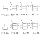
- FIGS. 3A-D are side views of a Si substrate 10 undergoing in-situ ammonia nitridation of an ultra-thin “dry-wet” DCE/O 2 —H 2 O/O 2 based ultra-thin gate dielectric, in an embodiment in accordance with the invention.
- FIG. 3A is a side view of a Si semiconductor substrate 10 .
- the substrate 10 is processed in a batch vertical diffusion furnace with a “dry ox” DCE/O 2 gas.
- FIG. 3B is a side view of the resulting substrate 30 showing a base gate dielectric 31 comprising a Cl layer 13 on the SiO 2 layer 14 .
- the substrate 30 is processed in-situ with H 2 O/O 2 gas (wet ox).
- FIG. 3C is a side view of the resulting substrate 32 showing a dielectric 33 comprising a Cl layer 13 on a SiO 2 layer 14 .
- FIG. 3D is a side view of the resulting substrate 35 showing a dielectric 36 comprising an N layer 18 on a SiO 2 layer 14 .
- the DCE plays a critical role in the in-situ surface nitridation process as the incorporated Cl species is constrained to the surface of the grown gate oxide and undergoes a substitutional chemical reaction with the NH 3 species during the nitridation process.
- the substitutional chemistry between the C 1 and NH 3 species enables maximum nitrogen incorporation, constraining the nitridation to the surface of the gate dielectric.
- FIGS. 4A-D are side views of a Si substrate 10 undergoing in-situ ammonia nitridation of an ultra-thin “dry-wet” DCE/O 2 —H 2 O/O 2 based ultra-thin gate dielectric, in another embodiment in accordance with the invention.
- FIG. 4A is a side view of a Si semiconductor substrate 10 .
- the substrate 10 is processed in a batch vertical diffusion furnace with a “dry ox” DCE/O 2 gas.
- FIG. 4B is a side view of the resulting substrate 40 showing a base gate dielectric 41 comprising a Cl layer 13 on a SiO 2 layer 14 .
- the substrate 40 is processed in-situ with an ultra-dilute NH 3 /N 2 gas at a concentration of less than 1 E-7 moles NH 3 /mm 2 .
- FIG. 4C is a side view of the resulting substrate 42 showing a dielectric 43 comprising an N layer 18 on a SiO 2 layer 14 .
- the substrate 42 is processed in-situ with H 2 O/O 2 gas (wet ox).
- FIG. 4D is a side view of the resulting substrate 44 showing a dielectric 46 comprising an N layer 18 on a SiO 2 layer 14 .
- a gate dielectric can be chemically tailored to incorporate different levels of nitridation at the gate dielectric surface, and alter the edge to area leakage characteristics to accommodate different CMOS technology transistor requirements.
- FIG. 5 present data comparing the performance of an ultra-thin DCE based gate oxide with in-situ nitridation with the performance of traditional ex-situ rapid thermal anneal (RTA) processing for both 13 ⁇ m and 0.09 ⁇ m technologies.
- the ultra-thin chemically tailored gate dielectrics generated in vertical diffusion furnace with ultra-dilute NH 3 , below 1E-7 moles NH 3 /mm 2 , in-situ nitridation show a performance comparable or better to traditional ex-situ rapid thermal anneal (RTA) processing techniques for 90 nm CMOS technology.
- RTA rapid thermal anneal
- FIG. 6 is a representation of a vertical diffusion furnace 60 (VDF) for in-situ nitridation and growth of ultra-thin gate dielectrics, in accordance with an embodiment of the present invention.
- the VDF is particularly useful for nitridation via an NH 3 (ammonia) or NO (Nitric Oxide) source.
- the VDF comprises: a RHC (rapid heat/rapid cool) thermal apparatus 61 ; an external pyro torch for DCE cracking 62 ; catalytic water (steam) vapor generator 63 ; NO (nitric oxide) source 64 ; NH 3 (ammonia) source 65 ; and N 2 reactor chamber dilution source.
- the semiconductor substrate are held horizontally in a frame 68 , and are processed in a reaction chamber 69 .
- the VDF 60 comprises: an NO (nitric oxide) source 64 with a flow rate of less than 50 sccms; NH 3 (ammonia) source 65 with a flow rate of less than 50 sccms; and N 2 reactor chamber dilution source greater than 25 slm.
- the VDF 60 is an atmospheric system capable of processing multiple substrates 67 (batch) with rapid heating and cooling up to temperatures of 1100° C.
- the substrates 67 are inserted into the reactor chamber 69 where they are oxidized at temperatures between 500° C.-750° C. Subsequently, the oxidized or re-oxidized substrates 67 are thermally ramped to temperatures between 700° C.-975° C. and annealed in-situ with an ultra-dilute NH 3 /N 2 gas at a concentration of less than 1E-7 moles NH 3 /mm 2 .
- the substrates 67 are cooled using a rapid heat/rapid cool thermal apparatus to a temperature below 700° C. where the final NH 3 /O 2 gas (wet ox) treatment is conducted.
- the substrates 67 are removed from the reactor chamber 69 at a temperature below 700° C. All processing steps occur under atmospheric conditions, in accordance with the methods of the present invention.
Landscapes
- Engineering & Computer Science (AREA)
- Microelectronics & Electronic Packaging (AREA)
- Power Engineering (AREA)
- General Physics & Mathematics (AREA)
- Computer Hardware Design (AREA)
- Physics & Mathematics (AREA)
- Condensed Matter Physics & Semiconductors (AREA)
- Manufacturing & Machinery (AREA)
- Chemical & Material Sciences (AREA)
- Chemical Kinetics & Catalysis (AREA)
- Crystallography & Structural Chemistry (AREA)
- General Chemical & Material Sciences (AREA)
- Ceramic Engineering (AREA)
- Formation Of Insulating Films (AREA)
- Insulated Gate Type Field-Effect Transistor (AREA)
Abstract
Description
Claims (22)
Priority Applications (1)
| Application Number | Priority Date | Filing Date | Title |
|---|---|---|---|
| US10/339,783 US6808993B2 (en) | 2003-01-08 | 2003-01-08 | Ultra-thin gate dielectrics |
Applications Claiming Priority (1)
| Application Number | Priority Date | Filing Date | Title |
|---|---|---|---|
| US10/339,783 US6808993B2 (en) | 2003-01-08 | 2003-01-08 | Ultra-thin gate dielectrics |
Publications (2)
| Publication Number | Publication Date |
|---|---|
| US20040132316A1 US20040132316A1 (en) | 2004-07-08 |
| US6808993B2 true US6808993B2 (en) | 2004-10-26 |
Family
ID=32681546
Family Applications (1)
| Application Number | Title | Priority Date | Filing Date |
|---|---|---|---|
| US10/339,783 Expired - Lifetime US6808993B2 (en) | 2003-01-08 | 2003-01-08 | Ultra-thin gate dielectrics |
Country Status (1)
| Country | Link |
|---|---|
| US (1) | US6808993B2 (en) |
Cited By (4)
| Publication number | Priority date | Publication date | Assignee | Title |
|---|---|---|---|---|
| US20060148179A1 (en) * | 2005-01-03 | 2006-07-06 | Yu-Ren Wang | Method of fabricating nitrogen-containing gate dielectric layer and semiconductor device |
| US20080102650A1 (en) * | 2006-10-30 | 2008-05-01 | Edward Dennis Adams | Method of fabricating a nitrided silicon oxide gate dielectric layer |
| US20090206406A1 (en) * | 2008-02-15 | 2009-08-20 | Willy Rachmady | Multi-gate device having a t-shaped gate structure |
| CN102820207A (en) * | 2011-06-11 | 2012-12-12 | 中国科学院微电子研究所 | Method and device for avoiding chloroethylene failure of oxidation furnace tube |
Families Citing this family (2)
| Publication number | Priority date | Publication date | Assignee | Title |
|---|---|---|---|---|
| US20090085082A1 (en) * | 2007-09-27 | 2009-04-02 | Gilbert Dewey | Controlled intermixing of hfo2 and zro2 dielectrics enabling higher dielectric constant and reduced gate leakage |
| CN107305842B (en) * | 2016-04-25 | 2021-08-17 | 联华电子股份有限公司 | Method for manufacturing gate dielectric layer |
Citations (4)
| Publication number | Priority date | Publication date | Assignee | Title |
|---|---|---|---|---|
| US6124171A (en) | 1998-09-24 | 2000-09-26 | Intel Corporation | Method of forming gate oxide having dual thickness by oxidation process |
| US6239044B1 (en) * | 1998-06-08 | 2001-05-29 | Sony Corporation | Apparatus for forming silicon oxide film and method of forming silicon oxide film |
| US6265297B1 (en) * | 1999-09-01 | 2001-07-24 | Micron Technology, Inc. | Ammonia passivation of metal gate electrodes to inhibit oxidation of metal |
| US6670242B1 (en) * | 1999-06-24 | 2003-12-30 | Agere Systems Inc. | Method for making an integrated circuit device including a graded, grown, high quality gate oxide layer and a nitride layer |
-
2003
- 2003-01-08 US US10/339,783 patent/US6808993B2/en not_active Expired - Lifetime
Patent Citations (4)
| Publication number | Priority date | Publication date | Assignee | Title |
|---|---|---|---|---|
| US6239044B1 (en) * | 1998-06-08 | 2001-05-29 | Sony Corporation | Apparatus for forming silicon oxide film and method of forming silicon oxide film |
| US6124171A (en) | 1998-09-24 | 2000-09-26 | Intel Corporation | Method of forming gate oxide having dual thickness by oxidation process |
| US6670242B1 (en) * | 1999-06-24 | 2003-12-30 | Agere Systems Inc. | Method for making an integrated circuit device including a graded, grown, high quality gate oxide layer and a nitride layer |
| US6265297B1 (en) * | 1999-09-01 | 2001-07-24 | Micron Technology, Inc. | Ammonia passivation of metal gate electrodes to inhibit oxidation of metal |
Non-Patent Citations (2)
| Title |
|---|
| "Promecon (TM) 1000 [vertical furnace installation], " Sizary Products, http://www.sizary.com/products_P1000_vert.htm, Jul. 25, 2001, 3 pgs. |
| Peters, Laura, "Thermal Processing's Tool of Choice: Single-Wafer RTP or Fast Ramp Batch?" Semiconductor International, Jan. 1, 1998, 6 pgs. |
Cited By (8)
| Publication number | Priority date | Publication date | Assignee | Title |
|---|---|---|---|---|
| US20060148179A1 (en) * | 2005-01-03 | 2006-07-06 | Yu-Ren Wang | Method of fabricating nitrogen-containing gate dielectric layer and semiconductor device |
| US7312139B2 (en) * | 2005-01-03 | 2007-12-25 | United Microelectronics Corp. | Method of fabricating nitrogen-containing gate dielectric layer and semiconductor device |
| US20080102650A1 (en) * | 2006-10-30 | 2008-05-01 | Edward Dennis Adams | Method of fabricating a nitrided silicon oxide gate dielectric layer |
| US7737050B2 (en) | 2006-10-30 | 2010-06-15 | International Business Machines Corporation | Method of fabricating a nitrided silicon oxide gate dielectric layer |
| US20090206406A1 (en) * | 2008-02-15 | 2009-08-20 | Willy Rachmady | Multi-gate device having a t-shaped gate structure |
| US8264048B2 (en) | 2008-02-15 | 2012-09-11 | Intel Corporation | Multi-gate device having a T-shaped gate structure |
| CN102820207A (en) * | 2011-06-11 | 2012-12-12 | 中国科学院微电子研究所 | Method and device for avoiding chloroethylene failure of oxidation furnace tube |
| CN102820207B (en) * | 2011-06-11 | 2015-09-23 | 中国科学院微电子研究所 | Method and device for avoiding chloroethylene failure of oxidation furnace tube |
Also Published As
| Publication number | Publication date |
|---|---|
| US20040132316A1 (en) | 2004-07-08 |
Similar Documents
| Publication | Publication Date | Title |
|---|---|---|
| JP5072837B2 (en) | Improved manufacturing method for annealing a plasma-nitrided gate dielectric in two steps after nitridation | |
| KR101014938B1 (en) | Silicon oxynitride gate dielectric formation using multiple annealing steps | |
| KR101058882B1 (en) | Nitrogen Profile Tailoring of Silicon Oxynitrides by Rapid Thermal Annealing with Ammonia at Ultra-Low Pressure | |
| US20080090425A9 (en) | Two-step post nitridation annealing for lower EOT plasma nitrided gate dielectrics | |
| KR101286309B1 (en) | Replacement metal gate transistors with reduced gate oxide leakage | |
| WO2012018975A2 (en) | Mos transistors including sion gate dielectric with enhanced nitrogen concentration at its sidewalls | |
| US7514376B2 (en) | Manufacture of semiconductor device having nitridized insulating film | |
| JP2005166696A (en) | Metallic compound thin film, manufacturing method therefor, semiconductor device including the same and manufacturing method therefor | |
| JP3593340B2 (en) | Manufacturing method of integrated circuit device | |
| US6808993B2 (en) | Ultra-thin gate dielectrics | |
| US20060148179A1 (en) | Method of fabricating nitrogen-containing gate dielectric layer and semiconductor device | |
| JP4762169B2 (en) | Manufacturing method of semiconductor device | |
| JP3399413B2 (en) | Oxynitride film and method for forming the same | |
| JP2007142024A (en) | Method of manufacturing semiconductor device | |
| US6221789B1 (en) | Thin oxides of silicon | |
| US6407008B1 (en) | Method of forming an oxide layer | |
| JP2000243752A (en) | Method of forming silicon nitride oxide film and manufacture for p-type semiconductor element | |
| JP5119904B2 (en) | Manufacturing method of semiconductor device | |
| JP5121142B2 (en) | Manufacturing method of semiconductor device | |
| JP2006319137A (en) | Semiconductor device and its manufacturing method | |
| JP3357815B2 (en) | Method for manufacturing semiconductor device | |
| JP2000269490A (en) | Manufacture of semiconductor device | |
| JPH11297690A (en) | Formation of gate insulating film | |
| JP2005150285A (en) | Method of manufacturing semiconductor device | |
| JPH07135206A (en) | Oxide film forming method |
Legal Events
| Date | Code | Title | Description |
|---|---|---|---|
| AS | Assignment |
Owner name: INTEL CORPORATION, CALIFORNIA Free format text: ASSIGNMENT OF ASSIGNORS INTEREST;ASSIGNORS:FINNIE, CHRISTINE M.;LINDERT, NICK;ALTHOFF, KIRK;AND OTHERS;REEL/FRAME:014038/0474 Effective date: 20030425 |
|
| STCF | Information on status: patent grant |
Free format text: PATENTED CASE |
|
| FEPP | Fee payment procedure |
Free format text: PAYOR NUMBER ASSIGNED (ORIGINAL EVENT CODE: ASPN); ENTITY STATUS OF PATENT OWNER: LARGE ENTITY |
|
| CC | Certificate of correction | ||
| FPAY | Fee payment |
Year of fee payment: 4 |
|
| FPAY | Fee payment |
Year of fee payment: 8 |
|
| FPAY | Fee payment |
Year of fee payment: 12 |