US6800338B2 - Electro-optical liquid-crystal display - Google Patents
Electro-optical liquid-crystal display Download PDFInfo
- Publication number
- US6800338B2 US6800338B2 US09/834,762 US83476201A US6800338B2 US 6800338 B2 US6800338 B2 US 6800338B2 US 83476201 A US83476201 A US 83476201A US 6800338 B2 US6800338 B2 US 6800338B2
- Authority
- US
- United States
- Prior art keywords
- liquid
- carbon atoms
- crystal
- display according
- alignment layers
- Prior art date
- Legal status (The legal status is an assumption and is not a legal conclusion. Google has not performed a legal analysis and makes no representation as to the accuracy of the status listed.)
- Expired - Fee Related, expires
Links
- 0 [1*]c1cnc(-c2cc(C)c([2*])c(C)c2)nc1 Chemical compound [1*]c1cnc(-c2cc(C)c([2*])c(C)c2)nc1 0.000 description 34
- SPSITJRIKZHNML-UHFFFAOYSA-N C.C.C.C.C.C.CC1CCC(CCC2CCC(CC3CCC(CC4CCC(C)CC4)CC3)CC2)CC1 Chemical compound C.C.C.C.C.C.CC1CCC(CCC2CCC(CC3CCC(CC4CCC(C)CC4)CC3)CC2)CC1 SPSITJRIKZHNML-UHFFFAOYSA-N 0.000 description 3
- DKLCRRAJPZVKTH-UHFFFAOYSA-N Cc1cc(C2CCC(C)CC2)cc(C)c1C#N.II Chemical compound Cc1cc(C2CCC(C)CC2)cc(C)c1C#N.II DKLCRRAJPZVKTH-UHFFFAOYSA-N 0.000 description 3
- JCIZQQKWMNXWMW-UHFFFAOYSA-N Cc1ccc(C(=O)Oc2cc(C)c(C#N)c(F)c2)cc1 Chemical compound Cc1ccc(C(=O)Oc2cc(C)c(C#N)c(F)c2)cc1 JCIZQQKWMNXWMW-UHFFFAOYSA-N 0.000 description 3
- JHXJAWXZLWDDED-UHFFFAOYSA-N C=CC1CCC(c2ccc(C#N)cc2)CC1 Chemical compound C=CC1CCC(c2ccc(C#N)cc2)CC1 JHXJAWXZLWDDED-UHFFFAOYSA-N 0.000 description 2
- PYGSGIHPNBGSQU-UHFFFAOYSA-N CC1CCC(C)CC1.CC1CCC(C)CC1.CC1CCC(C)CC1.CC1CCC(C)CC1.CC1CCC(C)CC1.CC1COC(C)OC1.Cc1ccc(C)c(F)c1.Cc1ccc(C)c(F)c1.Cc1ccc(C)cc1.Cc1ccc(C)nc1.Cc1ccc(C)nc1.Cc1cnc(C)nc1 Chemical compound CC1CCC(C)CC1.CC1CCC(C)CC1.CC1CCC(C)CC1.CC1CCC(C)CC1.CC1CCC(C)CC1.CC1COC(C)OC1.Cc1ccc(C)c(F)c1.Cc1ccc(C)c(F)c1.Cc1ccc(C)cc1.Cc1ccc(C)nc1.Cc1ccc(C)nc1.Cc1cnc(C)nc1 PYGSGIHPNBGSQU-UHFFFAOYSA-N 0.000 description 2
- IFRMBICULWSWMO-UHFFFAOYSA-N C.C.C.C.C.C.C.C.C.CC1CCC(C)CC1.CC1CCC(C)CC1.CC1CCC(C)CC1.CC1CCC(C)CC1.CC1CCC(C)CC1.Cc1ccc(C)cc1 Chemical compound C.C.C.C.C.C.C.C.C.CC1CCC(C)CC1.CC1CCC(C)CC1.CC1CCC(C)CC1.CC1CCC(C)CC1.CC1CCC(C)CC1.Cc1ccc(C)cc1 IFRMBICULWSWMO-UHFFFAOYSA-N 0.000 description 1
- WCRWIHYZRRKDGF-UHFFFAOYSA-N C.C.C.C.C.C.C.C.CC1CCC(C)CC1.CC1CCC(C)CC1.CC1CCC(C)CC1.CC1CCC(C)CC1.CC1CCC(C)CC1 Chemical compound C.C.C.C.C.C.C.C.CC1CCC(C)CC1.CC1CCC(C)CC1.CC1CCC(C)CC1.CC1CCC(C)CC1.CC1CCC(C)CC1 WCRWIHYZRRKDGF-UHFFFAOYSA-N 0.000 description 1
- WMIFCOOBCQATKY-UHFFFAOYSA-N C.C.C.C.C.C.C.C.CC1CCC(CC2CCC(CC3CCC(CC4CCC(C)CC4)CC3)CC2)CC1 Chemical compound C.C.C.C.C.C.C.C.CC1CCC(CC2CCC(CC3CCC(CC4CCC(C)CC4)CC3)CC2)CC1 WMIFCOOBCQATKY-UHFFFAOYSA-N 0.000 description 1
- HZBUPDLZEOKWFD-UHFFFAOYSA-N C.C.C.C.C.C.C=CCC1CCC(C2CCC(CC=C)CC2)CC1 Chemical compound C.C.C.C.C.C.C=CCC1CCC(C2CCC(CC=C)CC2)CC1 HZBUPDLZEOKWFD-UHFFFAOYSA-N 0.000 description 1
- NSEVWWHEESPTBQ-UHFFFAOYSA-N C.C.C.C.C.C.CC1CCC(C)CC1.CC1CCC(C)CC1.CC1CCC(C)CC1.CC1CCC(C)CC1.CC1CCC(C)CC1.CC1COC(C)OC1.Cc1ccc(C)c(F)c1.Cc1ccc(C)c(F)c1.Cc1ccc(C)cc1.Cc1ccc(C)nc1.Cc1ccc(C)nc1.Cc1cnc(C)nc1 Chemical compound C.C.C.C.C.C.CC1CCC(C)CC1.CC1CCC(C)CC1.CC1CCC(C)CC1.CC1CCC(C)CC1.CC1CCC(C)CC1.CC1COC(C)OC1.Cc1ccc(C)c(F)c1.Cc1ccc(C)c(F)c1.Cc1ccc(C)cc1.Cc1ccc(C)nc1.Cc1ccc(C)nc1.Cc1cnc(C)nc1 NSEVWWHEESPTBQ-UHFFFAOYSA-N 0.000 description 1
- KWSPRHWNXPZCFF-UHFFFAOYSA-N C.C.C.C.C.C.CC1COC(C)OC1.Cc1ccc(C)c(F)c1.Cc1ccc(C)c(F)c1.Cc1ccc(C)cc1.Cc1ccc(C)nc1.Cc1ccc(C)nc1.Cc1cnc(C)nc1 Chemical compound C.C.C.C.C.C.CC1COC(C)OC1.Cc1ccc(C)c(F)c1.Cc1ccc(C)c(F)c1.Cc1ccc(C)cc1.Cc1ccc(C)nc1.Cc1ccc(C)nc1.Cc1cnc(C)nc1 KWSPRHWNXPZCFF-UHFFFAOYSA-N 0.000 description 1
- AJBKWLIVNOPVIO-UHFFFAOYSA-N C.C.C.C.C.CC1CCC(C2CCC(CC3CCC(C4CCC(C)CC4)CC3)CC2)CC1.CC1CCC(CC2CCC(C)CC2)CC1.CC1CCC(CC2CCC(C3CCC(C)CC3)CC2)CC1 Chemical compound C.C.C.C.C.CC1CCC(C2CCC(CC3CCC(C4CCC(C)CC4)CC3)CC2)CC1.CC1CCC(CC2CCC(C)CC2)CC1.CC1CCC(CC2CCC(C3CCC(C)CC3)CC2)CC1 AJBKWLIVNOPVIO-UHFFFAOYSA-N 0.000 description 1
- GCKBANOJBOADPH-UHFFFAOYSA-N C.C.C.C.C.CC1COC(C)OC1.Cc1cc(F)c(C)c(F)c1.Cc1ccc(C)c(F)c1.Cc1ccc(C)cc1 Chemical compound C.C.C.C.C.CC1COC(C)OC1.Cc1cc(F)c(C)c(F)c1.Cc1ccc(C)c(F)c1.Cc1ccc(C)cc1 GCKBANOJBOADPH-UHFFFAOYSA-N 0.000 description 1
- PVGDLIYTVYSMIW-UHFFFAOYSA-N C.C.C.C.CC1CCC(C)CC1.CC1CCC(C)CC1.CC1CCC(C)CC1 Chemical compound C.C.C.C.CC1CCC(C)CC1.CC1CCC(C)CC1.CC1CCC(C)CC1 PVGDLIYTVYSMIW-UHFFFAOYSA-N 0.000 description 1
- RJTUFYLKYLRISR-UHFFFAOYSA-N C.C.C.C.CC1CCC(C)CC1.CC1CCC(C)CC1.Cc1ccc(C)cc1 Chemical compound C.C.C.C.CC1CCC(C)CC1.CC1CCC(C)CC1.Cc1ccc(C)cc1 RJTUFYLKYLRISR-UHFFFAOYSA-N 0.000 description 1
- QXHFVMNBAOMODB-UHFFFAOYSA-M C.C.C.C.Cc1cc(CC2CCC(CC3CCC(C)CC3)CC2)cc(C)c1C.[V]I Chemical compound C.C.C.C.Cc1cc(CC2CCC(CC3CCC(C)CC3)CC2)cc(C)c1C.[V]I QXHFVMNBAOMODB-UHFFFAOYSA-M 0.000 description 1
- WTAFVKCBOQTPTH-UHFFFAOYSA-N C.C.C.C=CCC1CCC(C2CCC(C=C)CC2)CC1 Chemical compound C.C.C.C=CCC1CCC(C2CCC(C=C)CC2)CC1 WTAFVKCBOQTPTH-UHFFFAOYSA-N 0.000 description 1
- ZORMPPBPNITURF-UHFFFAOYSA-N C.C.C.C=CCC1CCC(c2ccc(C#N)cc2)CC1 Chemical compound C.C.C.C=CCC1CCC(c2ccc(C#N)cc2)CC1 ZORMPPBPNITURF-UHFFFAOYSA-N 0.000 description 1
- WOJMBGCXIUCJIS-UHFFFAOYSA-N C.C.C.CC1CCC(C)CC1.CC1CCC(C)CC1 Chemical compound C.C.C.CC1CCC(C)CC1.CC1CCC(C)CC1 WOJMBGCXIUCJIS-UHFFFAOYSA-N 0.000 description 1
- INNIVNHKMFMXSV-UHFFFAOYSA-N C.C.C.CC=CCC1CCC(c2ccc(C#N)cc2)CC1 Chemical compound C.C.C.CC=CCC1CCC(c2ccc(C#N)cc2)CC1 INNIVNHKMFMXSV-UHFFFAOYSA-N 0.000 description 1
- GFEAPZIMBUOGCT-UHFFFAOYSA-M C.C.C.Cc1ccc(C#Cc2ccc(CC3CCC(C)CC3)cc2)cc1.[V]I Chemical compound C.C.C.Cc1ccc(C#Cc2ccc(CC3CCC(C)CC3)cc2)cc1.[V]I GFEAPZIMBUOGCT-UHFFFAOYSA-M 0.000 description 1
- XXRSWNHWOOBATO-UHFFFAOYSA-N C.C.C=Nc1ccc(OC(=O)c2ccc(COC)cc2)cc1F.Cc1ccc(C(=O)Oc2cc(F)c(C#N)c(F)c2)cc1.Cc1ccc(C(=O)Oc2ccc(C#N)c(F)c2)cc1 Chemical compound C.C.C=Nc1ccc(OC(=O)c2ccc(COC)cc2)cc1F.Cc1ccc(C(=O)Oc2cc(F)c(C#N)c(F)c2)cc1.Cc1ccc(C(=O)Oc2ccc(C#N)c(F)c2)cc1 XXRSWNHWOOBATO-UHFFFAOYSA-N 0.000 description 1
- WGUJGGKVKZJXLQ-UHFFFAOYSA-N C.C.CC1CCC(C)CC1.Cc1ccc(C)cc1 Chemical compound C.C.CC1CCC(C)CC1.Cc1ccc(C)cc1 WGUJGGKVKZJXLQ-UHFFFAOYSA-N 0.000 description 1
- KJBGMPWWCJVCLK-ONEGZZNKSA-N C/C=C/C1CCC(c2ccc(-c3ccc(C)cc3)cc2)CC1 Chemical compound C/C=C/C1CCC(c2ccc(-c3ccc(C)cc3)cc2)CC1 KJBGMPWWCJVCLK-ONEGZZNKSA-N 0.000 description 1
- OSEGRSWKSZYORA-ONEGZZNKSA-N C/C=C/CCC1CCC(c2ccc(-c3ccc(C)cc3)cc2)CC1 Chemical compound C/C=C/CCC1CCC(c2ccc(-c3ccc(C)cc3)cc2)CC1 OSEGRSWKSZYORA-ONEGZZNKSA-N 0.000 description 1
- INISWPBOLQGEGH-UHFFFAOYSA-N C=CC1CCC(C2CCC(C)CC2)CC1 Chemical compound C=CC1CCC(C2CCC(C)CC2)CC1 INISWPBOLQGEGH-UHFFFAOYSA-N 0.000 description 1
- JHYHMRZAJLCIHW-UHFFFAOYSA-N C=CC1CCC(C2CCC(C=C)CC2)CC1 Chemical compound C=CC1CCC(C2CCC(C=C)CC2)CC1 JHYHMRZAJLCIHW-UHFFFAOYSA-N 0.000 description 1
- FVVMZDMDPCZGFP-UHFFFAOYSA-N C=CC1CCC(C2CCC(C=CC)CC2)CC1 Chemical compound C=CC1CCC(C2CCC(C=CC)CC2)CC1 FVVMZDMDPCZGFP-UHFFFAOYSA-N 0.000 description 1
- BCUMFFLWJNKNOU-UHFFFAOYSA-N C=CC1CCC(C2CCC(c3ccc(C)cc3)CC2)CC1 Chemical compound C=CC1CCC(C2CCC(c3ccc(C)cc3)CC2)CC1 BCUMFFLWJNKNOU-UHFFFAOYSA-N 0.000 description 1
- ALFLDQIYGBNZCO-UHFFFAOYSA-N C=CC1CCC(C2CCC(c3ccc(F)c(F)c3)CC2)CC1 Chemical compound C=CC1CCC(C2CCC(c3ccc(F)c(F)c3)CC2)CC1 ALFLDQIYGBNZCO-UHFFFAOYSA-N 0.000 description 1
- MZPXJRMYFGDCSL-UHFFFAOYSA-N C=CC1CCC(c2ccc(-c3ccc(C)cc3)cc2)CC1 Chemical compound C=CC1CCC(c2ccc(-c3ccc(C)cc3)cc2)CC1 MZPXJRMYFGDCSL-UHFFFAOYSA-N 0.000 description 1
- ZWDLVDAOTSTTNH-UHFFFAOYSA-N C=CCC1CCC(C2CCC(C)CC2)CC1.C=CCC1CCC(C2CCC(CC=C)CC2)CC1.CC1CCC(C2CCC(C)CC2)CC1.COC1CCC(C2CCC(C)CC2)CC1 Chemical compound C=CCC1CCC(C2CCC(C)CC2)CC1.C=CCC1CCC(C2CCC(CC=C)CC2)CC1.CC1CCC(C2CCC(C)CC2)CC1.COC1CCC(C2CCC(C)CC2)CC1 ZWDLVDAOTSTTNH-UHFFFAOYSA-N 0.000 description 1
- LBVKJXXREKNHCM-UHFFFAOYSA-N C=CCC1CCC(c2ccc(-c3ccc(C)cc3)cc2)CC1 Chemical compound C=CCC1CCC(c2ccc(-c3ccc(C)cc3)cc2)CC1 LBVKJXXREKNHCM-UHFFFAOYSA-N 0.000 description 1
- OXPUOKDPOMJNKA-UHFFFAOYSA-N C=CCCC1CCC(C2CCC(c3ccc(C)cc3)CC2)CC1 Chemical compound C=CCCC1CCC(C2CCC(c3ccc(C)cc3)CC2)CC1 OXPUOKDPOMJNKA-UHFFFAOYSA-N 0.000 description 1
- GDCDKEVEFPFLRM-UHFFFAOYSA-N CC#COC1CCC(C2CCC(C)CC2)CC1 Chemical compound CC#COC1CCC(C2CCC(C)CC2)CC1 GDCDKEVEFPFLRM-UHFFFAOYSA-N 0.000 description 1
- XVTNSOOKHDCYKH-PHEQNACWSA-N CC1CCC(/C=C/C2CCC(/C=C/C3CCC(C)CC3)CC2)CC1 Chemical compound CC1CCC(/C=C/C2CCC(/C=C/C3CCC(C)CC3)CC2)CC1 XVTNSOOKHDCYKH-PHEQNACWSA-N 0.000 description 1
- DVZSFMHCSUGJJF-MDZDMXLPSA-N CC1CCC(/C=C/C2CCC(C3CCC(C)CC3)CC2)CC1 Chemical compound CC1CCC(/C=C/C2CCC(C3CCC(C)CC3)CC2)CC1 DVZSFMHCSUGJJF-MDZDMXLPSA-N 0.000 description 1
- LLRRZTVJWKMDGF-UHFFFAOYSA-N CC1CCC(C(=O)Oc2cc(F)c(C#N)c(F)c2)CC1.CC1CCC(C(=O)Oc2ccc(C#N)c(F)c2)CC1.CC1CCC(C(=O)Oc2ccc(C#N)cc2)CC1.CC1CCC(CCc2cc(F)c(C#N)c(F)c2)CC1.CC1CCC(CCc2ccc(C#N)c(F)c2)CC1.CC1CCC(CCc2ccc(C#N)cc2)CC1 Chemical compound CC1CCC(C(=O)Oc2cc(F)c(C#N)c(F)c2)CC1.CC1CCC(C(=O)Oc2ccc(C#N)c(F)c2)CC1.CC1CCC(C(=O)Oc2ccc(C#N)cc2)CC1.CC1CCC(CCc2cc(F)c(C#N)c(F)c2)CC1.CC1CCC(CCc2ccc(C#N)c(F)c2)CC1.CC1CCC(CCc2ccc(C#N)cc2)CC1 LLRRZTVJWKMDGF-UHFFFAOYSA-N 0.000 description 1
- LLEFIRNHFTUVNT-UHFFFAOYSA-N CC1CCC(C2CCC(C(=O)Oc3cc(F)c(F)c(F)c3)CC2)CC1.CC1CCC(C2CCC(c3ccc(F)c(F)c3)CC2)CC1.CC1CCC(C2CCC(c3ccc(F)cc3)CC2)CC1.CC1CCC(CCc2ccc(F)c(F)c2)CC1.CC1CCC(c2cc(F)c(F)c(F)c2)CC1.CC1CCC(c2ccc(-c3cc(F)c(F)c(F)c3)c(F)c2)CC1.CC1CCC(c2ccc(-c3ccc(F)c(F)c3)cc2)CC1.CC1CCC(c2ccc(C(=O)Oc3cc(F)c(F)c(F)c3)cc2)CC1.CC1CCC(c2ccc(F)c(F)c2)CC1.CC1CCC(c2ccc(F)cc2)CC1 Chemical compound CC1CCC(C2CCC(C(=O)Oc3cc(F)c(F)c(F)c3)CC2)CC1.CC1CCC(C2CCC(c3ccc(F)c(F)c3)CC2)CC1.CC1CCC(C2CCC(c3ccc(F)cc3)CC2)CC1.CC1CCC(CCc2ccc(F)c(F)c2)CC1.CC1CCC(c2cc(F)c(F)c(F)c2)CC1.CC1CCC(c2ccc(-c3cc(F)c(F)c(F)c3)c(F)c2)CC1.CC1CCC(c2ccc(-c3ccc(F)c(F)c3)cc2)CC1.CC1CCC(c2ccc(C(=O)Oc3cc(F)c(F)c(F)c3)cc2)CC1.CC1CCC(c2ccc(F)c(F)c2)CC1.CC1CCC(c2ccc(F)cc2)CC1 LLEFIRNHFTUVNT-UHFFFAOYSA-N 0.000 description 1
- PJUAFLKBQAKDFY-UHFFFAOYSA-N CC1CCC(C2CCC(C)CC2)CC1.Cc1ccc(C2CCC(C)CC2)cc1 Chemical compound CC1CCC(C2CCC(C)CC2)CC1.Cc1ccc(C2CCC(C)CC2)cc1 PJUAFLKBQAKDFY-UHFFFAOYSA-N 0.000 description 1
- WNOIABIPQKODBY-UHFFFAOYSA-N CC1CCC(CCC2CCC(C)CC2)CC1 Chemical compound CC1CCC(CCC2CCC(C)CC2)CC1 WNOIABIPQKODBY-UHFFFAOYSA-N 0.000 description 1
- GGJNXEWYOVFBDN-UHFFFAOYSA-N CC1CCC(CCc2ccc(-c3ccc(C4CCC(C)CC4)cc3)cc2)CC1 Chemical compound CC1CCC(CCc2ccc(-c3ccc(C4CCC(C)CC4)cc3)cc2)CC1 GGJNXEWYOVFBDN-UHFFFAOYSA-N 0.000 description 1
- KXOOHUNXYVAMSS-UHFFFAOYSA-N CC1CCC(CCc2ccc(C#N)cc2)CC1 Chemical compound CC1CCC(CCc2ccc(C#N)cc2)CC1 KXOOHUNXYVAMSS-UHFFFAOYSA-N 0.000 description 1
- LYEGRKIYVVNGIY-UHFFFAOYSA-N CC1CCC(COOc2ccc(C3CCC(C)CC3)cc2)CC1 Chemical compound CC1CCC(COOc2ccc(C3CCC(C)CC3)cc2)CC1 LYEGRKIYVVNGIY-UHFFFAOYSA-N 0.000 description 1
- RYHGAAYQUPRDPQ-UHFFFAOYSA-N CC1CCC(OC(=O)C2CCC(C)CC2)CC1 Chemical compound CC1CCC(OC(=O)C2CCC(C)CC2)CC1 RYHGAAYQUPRDPQ-UHFFFAOYSA-N 0.000 description 1
- JFTVIVZHQMBCLR-UHFFFAOYSA-N CC1CCC(OC(=O)C2CCC(C3CCC(C)CC3)CC2)CC1 Chemical compound CC1CCC(OC(=O)C2CCC(C3CCC(C)CC3)CC2)CC1 JFTVIVZHQMBCLR-UHFFFAOYSA-N 0.000 description 1
- PPYYQGHVIQGKDR-UHFFFAOYSA-N CC1CCC(OC(=O)C2CCC(C3CCC(C)CC3)CC2)CC1.CC1CCC(c2ccc(-c3ccc(C4CCC(C)CC4)cc3)cc2)CC1.CC1CCC(c2ccc(-c3ccc(C4CCC(C)CC4)cc3F)cc2)CC1.CC1CCC(c2ccc(OC(=O)C3CCC(C4CCC(C)CC4)CC3)cc2)CC1.Cc1ccc(C2CCC(C)CC2)cc1.Cc1ccc(C2CCC(C3CCC(C)CC3)CC2)cc1.Cc1ccc(C2CCC(C3CCC(C4CCC(C)CC4)CC3)CC2)cc1.Cc1ccc(C2CCC(CCC3CCC(C)CC3)CC2)cc1.Cc1ccc(CCC2CCC(C3CCC(C)CC3)CC2)cc1.Cc1ccc(OC(=O)C2CCC(C3CCC(C)CC3)CC2)cc1 Chemical compound CC1CCC(OC(=O)C2CCC(C3CCC(C)CC3)CC2)CC1.CC1CCC(c2ccc(-c3ccc(C4CCC(C)CC4)cc3)cc2)CC1.CC1CCC(c2ccc(-c3ccc(C4CCC(C)CC4)cc3F)cc2)CC1.CC1CCC(c2ccc(OC(=O)C3CCC(C4CCC(C)CC4)CC3)cc2)CC1.Cc1ccc(C2CCC(C)CC2)cc1.Cc1ccc(C2CCC(C3CCC(C)CC3)CC2)cc1.Cc1ccc(C2CCC(C3CCC(C4CCC(C)CC4)CC3)CC2)cc1.Cc1ccc(C2CCC(CCC3CCC(C)CC3)CC2)cc1.Cc1ccc(CCC2CCC(C3CCC(C)CC3)CC2)cc1.Cc1ccc(OC(=O)C2CCC(C3CCC(C)CC3)CC2)cc1 PPYYQGHVIQGKDR-UHFFFAOYSA-N 0.000 description 1
- OOWHGAJZZJPJPX-UHFFFAOYSA-N CC1CCC(OC(=O)c2ccc(C3CCC(C)CC3)cc2)CC1 Chemical compound CC1CCC(OC(=O)c2ccc(C3CCC(C)CC3)cc2)CC1 OOWHGAJZZJPJPX-UHFFFAOYSA-N 0.000 description 1
- MRVIGGQIZGUNPJ-UHFFFAOYSA-N CC1CCC(c2cc(F)c(C#N)c(F)c2)CC1.CC1CCC(c2ccc(C#N)c(F)c2)CC1.CC1CCC(c2ccc(C#N)cc2)CC1 Chemical compound CC1CCC(c2cc(F)c(C#N)c(F)c2)CC1.CC1CCC(c2ccc(C#N)c(F)c2)CC1.CC1CCC(c2ccc(C#N)cc2)CC1 MRVIGGQIZGUNPJ-UHFFFAOYSA-N 0.000 description 1
- KSOKWHKGJLDMBC-UHFFFAOYSA-N CC1CCC(c2ccc(-c3ccc(C4CCC(C)CC4)cc3F)cc2)CC1 Chemical compound CC1CCC(c2ccc(-c3ccc(C4CCC(C)CC4)cc3F)cc2)CC1 KSOKWHKGJLDMBC-UHFFFAOYSA-N 0.000 description 1
- IULWJSCTPKQWLV-UHFFFAOYSA-N CC1CCC(c2ccc(CCC3CCC(C4CCC(C)CC4)CC3)cc2)CC1 Chemical compound CC1CCC(c2ccc(CCC3CCC(C4CCC(C)CC4)CC3)cc2)CC1 IULWJSCTPKQWLV-UHFFFAOYSA-N 0.000 description 1
- WKQAMNGFAAFSOC-UHFFFAOYSA-N CC1CCC(c2ccc(OC(=O)C3CCC(C4CCC(C)CC4)CC3)cc2)CC1 Chemical compound CC1CCC(c2ccc(OC(=O)C3CCC(C4CCC(C)CC4)CC3)cc2)CC1 WKQAMNGFAAFSOC-UHFFFAOYSA-N 0.000 description 1
- INDIWWBFPCCGNS-UHFFFAOYSA-N CC=CC1CCC(C2CCC(C=CC)CC2)CC1 Chemical compound CC=CC1CCC(C2CCC(C=CC)CC2)CC1 INDIWWBFPCCGNS-UHFFFAOYSA-N 0.000 description 1
- WFVBLRKVRNUULX-UHFFFAOYSA-N CC=CC1CCC(c2ccc(C#N)cc2)CC1 Chemical compound CC=CC1CCC(c2ccc(C#N)cc2)CC1 WFVBLRKVRNUULX-UHFFFAOYSA-N 0.000 description 1
- WBUQBWQWNDKJJR-UHFFFAOYSA-N CCC(C)COc1ccc(-c2ccc(C#N)cc2)cc1 Chemical compound CCC(C)COc1ccc(-c2ccc(C#N)cc2)cc1 WBUQBWQWNDKJJR-UHFFFAOYSA-N 0.000 description 1
- DNJQGRFZQMOYGM-UHFFFAOYSA-N CCC(C)Cc1ccc(-c2ccc(C#N)cc2)cc1 Chemical compound CCC(C)Cc1ccc(-c2ccc(C#N)cc2)cc1 DNJQGRFZQMOYGM-UHFFFAOYSA-N 0.000 description 1
- OYZITXKNUGHHKV-UHFFFAOYSA-N CCC1CCC(C(=O)Oc2ccc(-c3ccc(C#N)cc3)cc2)CC1 Chemical compound CCC1CCC(C(=O)Oc2ccc(-c3ccc(C#N)cc3)cc2)CC1 OYZITXKNUGHHKV-UHFFFAOYSA-N 0.000 description 1
- AITQOXOBSMXBRV-UHFFFAOYSA-N CCCCCc1ccc(-c2ccc(-c3ccc(C#N)cc3)cc2)cc1 Chemical compound CCCCCc1ccc(-c2ccc(-c3ccc(C#N)cc3)cc2)cc1 AITQOXOBSMXBRV-UHFFFAOYSA-N 0.000 description 1
- ZGSRUHJPFMBPDS-UHFFFAOYSA-N COCC1CCC(C2CCC(C)CC2)CC1 Chemical compound COCC1CCC(C2CCC(C)CC2)CC1 ZGSRUHJPFMBPDS-UHFFFAOYSA-N 0.000 description 1
- RINYLKSNGRLNCU-UHFFFAOYSA-N COc1ccc(-c2ccc(C#N)cc2)cc1 Chemical compound COc1ccc(-c2ccc(C#N)cc2)cc1 RINYLKSNGRLNCU-UHFFFAOYSA-N 0.000 description 1
- NXIQTICRGSVAKI-UHFFFAOYSA-N Cc1cc(CC2CCC(C)CC2)cc(C)c1C#N.[V] Chemical compound Cc1cc(CC2CCC(C)CC2)cc(C)c1C#N.[V] NXIQTICRGSVAKI-UHFFFAOYSA-N 0.000 description 1
- UITRQTKOTSQCGX-UHFFFAOYSA-N Cc1cc(F)c(C#Cc2ccc(C3CCC(C)CC3)cc2)c(F)c1.Cc1ccc(-c2ccc(C#Cc3c(F)cc(C)cc3F)cc2)cc1.Cc1ccc(C#Cc2c(F)cc(C)cc2F)cc1.Cc1ccc(C#Cc2ccc(-c3ccc(C)cc3)cc2)cc1.Cc1ccc(C#Cc2ccc(C)c(F)c2F)cc1.Cc1ccc(C#Cc2ccc(C)cc2)cc1.Cc1ccc(C#Cc2ccc(C3CCC(C)CC3)cc2)c(F)c1F.Cc1ccc(C#Cc2ccc(C3CCC(C)CC3)cc2)cc1.Cc1ccc(C#Cc2ccc(CCC3CCC(C)CC3)cc2)cc1 Chemical compound Cc1cc(F)c(C#Cc2ccc(C3CCC(C)CC3)cc2)c(F)c1.Cc1ccc(-c2ccc(C#Cc3c(F)cc(C)cc3F)cc2)cc1.Cc1ccc(C#Cc2c(F)cc(C)cc2F)cc1.Cc1ccc(C#Cc2ccc(-c3ccc(C)cc3)cc2)cc1.Cc1ccc(C#Cc2ccc(C)c(F)c2F)cc1.Cc1ccc(C#Cc2ccc(C)cc2)cc1.Cc1ccc(C#Cc2ccc(C3CCC(C)CC3)cc2)c(F)c1F.Cc1ccc(C#Cc2ccc(C3CCC(C)CC3)cc2)cc1.Cc1ccc(C#Cc2ccc(CCC3CCC(C)CC3)cc2)cc1 UITRQTKOTSQCGX-UHFFFAOYSA-N 0.000 description 1
- CGRKJGAKPDOBRB-UHFFFAOYSA-N Cc1ccc(-c2ccc(-c3ccc(C#N)cc3)cc2F)cc1 Chemical compound Cc1ccc(-c2ccc(-c3ccc(C#N)cc3)cc2F)cc1 CGRKJGAKPDOBRB-UHFFFAOYSA-N 0.000 description 1
- QLSNVABODCOLNS-UHFFFAOYSA-N Cc1ccc(-c2ccc(C#N)cc2)c(F)c1 Chemical compound Cc1ccc(-c2ccc(C#N)cc2)c(F)c1 QLSNVABODCOLNS-UHFFFAOYSA-N 0.000 description 1
- QIBWMVSMTSYUSK-UHFFFAOYSA-N Cc1ccc(-c2ccc(C#N)cc2)cc1 Chemical compound Cc1ccc(-c2ccc(C#N)cc2)cc1 QIBWMVSMTSYUSK-UHFFFAOYSA-N 0.000 description 1
- COZVOEWJRCIRIN-UHFFFAOYSA-N Cc1ccc(-c2ccc(C3CCC(C)(C#N)CC3)cc2)cc1 Chemical compound Cc1ccc(-c2ccc(C3CCC(C)(C#N)CC3)cc2)cc1 COZVOEWJRCIRIN-UHFFFAOYSA-N 0.000 description 1
- OQUSEJWKMSUWAK-UHFFFAOYSA-N Cc1ccc(-c2ccc(CCC3CCC(C)CC3)cc2)c(F)c1 Chemical compound Cc1ccc(-c2ccc(CCC3CCC(C)CC3)cc2)c(F)c1 OQUSEJWKMSUWAK-UHFFFAOYSA-N 0.000 description 1
- GTCBJIWYUZTREV-MDZDMXLPSA-N Cc1ccc(C2CCC(/C=C/C3CCC(C)CC3)CC2)cc1 Chemical compound Cc1ccc(C2CCC(/C=C/C3CCC(C)CC3)CC2)cc1 GTCBJIWYUZTREV-MDZDMXLPSA-N 0.000 description 1
- VGPUNBKDHUPPIT-UHFFFAOYSA-N Cc1ccc(C2CCC(C)CC2)c(F)c1F Chemical compound Cc1ccc(C2CCC(C)CC2)c(F)c1F VGPUNBKDHUPPIT-UHFFFAOYSA-N 0.000 description 1
- HJLUUORXWKAPHX-UHFFFAOYSA-N Cc1ccc(C2CCC(C3CCC(C)CC3)CC2)c(F)c1F Chemical compound Cc1ccc(C2CCC(C3CCC(C)CC3)CC2)c(F)c1F HJLUUORXWKAPHX-UHFFFAOYSA-N 0.000 description 1
Classifications
-
- G—PHYSICS
- G02—OPTICS
- G02F—OPTICAL DEVICES OR ARRANGEMENTS FOR THE CONTROL OF LIGHT BY MODIFICATION OF THE OPTICAL PROPERTIES OF THE MEDIA OF THE ELEMENTS INVOLVED THEREIN; NON-LINEAR OPTICS; FREQUENCY-CHANGING OF LIGHT; OPTICAL LOGIC ELEMENTS; OPTICAL ANALOGUE/DIGITAL CONVERTERS
- G02F1/00—Devices or arrangements for the control of the intensity, colour, phase, polarisation or direction of light arriving from an independent light source, e.g. switching, gating or modulating; Non-linear optics
- G02F1/01—Devices or arrangements for the control of the intensity, colour, phase, polarisation or direction of light arriving from an independent light source, e.g. switching, gating or modulating; Non-linear optics for the control of the intensity, phase, polarisation or colour
- G02F1/13—Devices or arrangements for the control of the intensity, colour, phase, polarisation or direction of light arriving from an independent light source, e.g. switching, gating or modulating; Non-linear optics for the control of the intensity, phase, polarisation or colour based on liquid crystals, e.g. single liquid crystal display cells
- G02F1/133—Constructional arrangements; Operation of liquid crystal cells; Circuit arrangements
- G02F1/1333—Constructional arrangements; Manufacturing methods
- G02F1/1337—Surface-induced orientation of the liquid crystal molecules, e.g. by alignment layers
- G02F1/133711—Surface-induced orientation of the liquid crystal molecules, e.g. by alignment layers by organic films, e.g. polymeric films
- G02F1/133723—Polyimide, polyamide-imide
-
- C—CHEMISTRY; METALLURGY
- C09—DYES; PAINTS; POLISHES; NATURAL RESINS; ADHESIVES; COMPOSITIONS NOT OTHERWISE PROVIDED FOR; APPLICATIONS OF MATERIALS NOT OTHERWISE PROVIDED FOR
- C09K—MATERIALS FOR MISCELLANEOUS APPLICATIONS, NOT PROVIDED FOR ELSEWHERE
- C09K19/00—Liquid crystal materials
- C09K19/04—Liquid crystal materials characterised by the chemical structure of the liquid crystal components, e.g. by a specific unit
- C09K19/42—Mixtures of liquid crystal compounds covered by two or more of the preceding groups C09K19/06 - C09K19/40
- C09K19/46—Mixtures of liquid crystal compounds covered by two or more of the preceding groups C09K19/06 - C09K19/40 containing esters
-
- C—CHEMISTRY; METALLURGY
- C09—DYES; PAINTS; POLISHES; NATURAL RESINS; ADHESIVES; COMPOSITIONS NOT OTHERWISE PROVIDED FOR; APPLICATIONS OF MATERIALS NOT OTHERWISE PROVIDED FOR
- C09K—MATERIALS FOR MISCELLANEOUS APPLICATIONS, NOT PROVIDED FOR ELSEWHERE
- C09K19/00—Liquid crystal materials
- C09K19/02—Liquid crystal materials characterised by optical, electrical or physical properties of the components, in general
- C09K19/0208—Twisted Nematic (T.N.); Super Twisted Nematic (S.T.N.); Optical Mode Interference (O.M.I.)
-
- C—CHEMISTRY; METALLURGY
- C09—DYES; PAINTS; POLISHES; NATURAL RESINS; ADHESIVES; COMPOSITIONS NOT OTHERWISE PROVIDED FOR; APPLICATIONS OF MATERIALS NOT OTHERWISE PROVIDED FOR
- C09K—MATERIALS FOR MISCELLANEOUS APPLICATIONS, NOT PROVIDED FOR ELSEWHERE
- C09K19/00—Liquid crystal materials
- C09K19/52—Liquid crystal materials characterised by components which are not liquid crystals, e.g. additives with special physical aspect: solvents, solid particles
- C09K19/54—Additives having no specific mesophase characterised by their chemical composition
- C09K19/56—Aligning agents
-
- G—PHYSICS
- G02—OPTICS
- G02F—OPTICAL DEVICES OR ARRANGEMENTS FOR THE CONTROL OF LIGHT BY MODIFICATION OF THE OPTICAL PROPERTIES OF THE MEDIA OF THE ELEMENTS INVOLVED THEREIN; NON-LINEAR OPTICS; FREQUENCY-CHANGING OF LIGHT; OPTICAL LOGIC ELEMENTS; OPTICAL ANALOGUE/DIGITAL CONVERTERS
- G02F1/00—Devices or arrangements for the control of the intensity, colour, phase, polarisation or direction of light arriving from an independent light source, e.g. switching, gating or modulating; Non-linear optics
- G02F1/01—Devices or arrangements for the control of the intensity, colour, phase, polarisation or direction of light arriving from an independent light source, e.g. switching, gating or modulating; Non-linear optics for the control of the intensity, phase, polarisation or colour
- G02F1/13—Devices or arrangements for the control of the intensity, colour, phase, polarisation or direction of light arriving from an independent light source, e.g. switching, gating or modulating; Non-linear optics for the control of the intensity, phase, polarisation or colour based on liquid crystals, e.g. single liquid crystal display cells
- G02F1/133—Constructional arrangements; Operation of liquid crystal cells; Circuit arrangements
- G02F1/1333—Constructional arrangements; Manufacturing methods
- G02F1/1337—Surface-induced orientation of the liquid crystal molecules, e.g. by alignment layers
- G02F1/133711—Surface-induced orientation of the liquid crystal molecules, e.g. by alignment layers by organic films, e.g. polymeric films
-
- C—CHEMISTRY; METALLURGY
- C08—ORGANIC MACROMOLECULAR COMPOUNDS; THEIR PREPARATION OR CHEMICAL WORKING-UP; COMPOSITIONS BASED THEREON
- C08G—MACROMOLECULAR COMPOUNDS OBTAINED OTHERWISE THAN BY REACTIONS ONLY INVOLVING UNSATURATED CARBON-TO-CARBON BONDS
- C08G73/00—Macromolecular compounds obtained by reactions forming a linkage containing nitrogen with or without oxygen or carbon in the main chain of the macromolecule, not provided for in groups C08G12/00 - C08G71/00
- C08G73/06—Polycondensates having nitrogen-containing heterocyclic rings in the main chain of the macromolecule
- C08G73/10—Polyimides; Polyester-imides; Polyamide-imides; Polyamide acids or similar polyimide precursors
-
- C—CHEMISTRY; METALLURGY
- C08—ORGANIC MACROMOLECULAR COMPOUNDS; THEIR PREPARATION OR CHEMICAL WORKING-UP; COMPOSITIONS BASED THEREON
- C08L—COMPOSITIONS OF MACROMOLECULAR COMPOUNDS
- C08L79/00—Compositions of macromolecular compounds obtained by reactions forming in the main chain of the macromolecule a linkage containing nitrogen with or without oxygen or carbon only, not provided for in groups C08L61/00 - C08L77/00
- C08L79/04—Polycondensates having nitrogen-containing heterocyclic rings in the main chain; Polyhydrazides; Polyamide acids or similar polyimide precursors
- C08L79/08—Polyimides; Polyester-imides; Polyamide-imides; Polyamide acids or similar polyimide precursors
-
- C—CHEMISTRY; METALLURGY
- C09—DYES; PAINTS; POLISHES; NATURAL RESINS; ADHESIVES; COMPOSITIONS NOT OTHERWISE PROVIDED FOR; APPLICATIONS OF MATERIALS NOT OTHERWISE PROVIDED FOR
- C09K—MATERIALS FOR MISCELLANEOUS APPLICATIONS, NOT PROVIDED FOR ELSEWHERE
- C09K2323/00—Functional layers of liquid crystal optical display excluding electroactive liquid crystal layer characterised by chemical composition
- C09K2323/02—Alignment layer characterised by chemical composition
- C09K2323/025—Polyamide
-
- C—CHEMISTRY; METALLURGY
- C09—DYES; PAINTS; POLISHES; NATURAL RESINS; ADHESIVES; COMPOSITIONS NOT OTHERWISE PROVIDED FOR; APPLICATIONS OF MATERIALS NOT OTHERWISE PROVIDED FOR
- C09K—MATERIALS FOR MISCELLANEOUS APPLICATIONS, NOT PROVIDED FOR ELSEWHERE
- C09K2323/00—Functional layers of liquid crystal optical display excluding electroactive liquid crystal layer characterised by chemical composition
- C09K2323/03—Viewing layer characterised by chemical composition
-
- G—PHYSICS
- G02—OPTICS
- G02F—OPTICAL DEVICES OR ARRANGEMENTS FOR THE CONTROL OF LIGHT BY MODIFICATION OF THE OPTICAL PROPERTIES OF THE MEDIA OF THE ELEMENTS INVOLVED THEREIN; NON-LINEAR OPTICS; FREQUENCY-CHANGING OF LIGHT; OPTICAL LOGIC ELEMENTS; OPTICAL ANALOGUE/DIGITAL CONVERTERS
- G02F1/00—Devices or arrangements for the control of the intensity, colour, phase, polarisation or direction of light arriving from an independent light source, e.g. switching, gating or modulating; Non-linear optics
- G02F1/01—Devices or arrangements for the control of the intensity, colour, phase, polarisation or direction of light arriving from an independent light source, e.g. switching, gating or modulating; Non-linear optics for the control of the intensity, phase, polarisation or colour
- G02F1/13—Devices or arrangements for the control of the intensity, colour, phase, polarisation or direction of light arriving from an independent light source, e.g. switching, gating or modulating; Non-linear optics for the control of the intensity, phase, polarisation or colour based on liquid crystals, e.g. single liquid crystal display cells
- G02F1/137—Devices or arrangements for the control of the intensity, colour, phase, polarisation or direction of light arriving from an independent light source, e.g. switching, gating or modulating; Non-linear optics for the control of the intensity, phase, polarisation or colour based on liquid crystals, e.g. single liquid crystal display cells characterised by the electro-optical or magneto-optical effect, e.g. field-induced phase transition, orientation effect, guest-host interaction or dynamic scattering
- G02F1/139—Devices or arrangements for the control of the intensity, colour, phase, polarisation or direction of light arriving from an independent light source, e.g. switching, gating or modulating; Non-linear optics for the control of the intensity, phase, polarisation or colour based on liquid crystals, e.g. single liquid crystal display cells characterised by the electro-optical or magneto-optical effect, e.g. field-induced phase transition, orientation effect, guest-host interaction or dynamic scattering based on orientation effects in which the liquid crystal remains transparent
- G02F1/1396—Devices or arrangements for the control of the intensity, colour, phase, polarisation or direction of light arriving from an independent light source, e.g. switching, gating or modulating; Non-linear optics for the control of the intensity, phase, polarisation or colour based on liquid crystals, e.g. single liquid crystal display cells characterised by the electro-optical or magneto-optical effect, e.g. field-induced phase transition, orientation effect, guest-host interaction or dynamic scattering based on orientation effects in which the liquid crystal remains transparent the liquid crystal being selectively controlled between a twisted state and a non-twisted state, e.g. TN-LC cell
- G02F1/1397—Devices or arrangements for the control of the intensity, colour, phase, polarisation or direction of light arriving from an independent light source, e.g. switching, gating or modulating; Non-linear optics for the control of the intensity, phase, polarisation or colour based on liquid crystals, e.g. single liquid crystal display cells characterised by the electro-optical or magneto-optical effect, e.g. field-induced phase transition, orientation effect, guest-host interaction or dynamic scattering based on orientation effects in which the liquid crystal remains transparent the liquid crystal being selectively controlled between a twisted state and a non-twisted state, e.g. TN-LC cell the twist being substantially higher than 90°, e.g. STN-, SBE-, OMI-LC cells
Definitions
- the present invention relates to electro-optical liquid-crystalline displays, in particular STN displays having low addressing voltages.
- liquid-crystal displays of this type the liquid crystals are used as dielectrics whose optical properties change reversibly on application of an electric voltage.
- Electro-optical displays which use liquid crystals as media are known to the person skilled in the art. These liquid-crystal displays use various electro-optical effects. The most common of these are the TN effect ( t wisted n ematic, having a homogeneous, virtually planar initial alignment of the liquid crystals and a nematic structure which is twisted by about 90°) and the STN effect ( s uper t wisted n ematic) and the SBE effect ( s uper t wisted b irefringence e ffect). In these and similar electro-optical effects, liquid-crystalline media of positive dielectric anisotropy ( ⁇ ) are used.
- STN displays which, in the present application, include all common and known types of display with relatively high twist, such as, for example, SBE ( s upertwisted b irefringent e ffect), GH (guest/host), STN and OMI (optical mode interference) displays, as well as compensated STN displays, such as DSTN ( d ouble layer STN) and film-compensated STN displays
- the liquid-crystal director is twisted from one side of the liquid-crystal layer to the other by a given angle of from greater than 90°, typically of 180° or more, up to 600°, typically up to 270°.
- a chiral liquid-crystal medium which consists of mesogenic chiral substances or, most widespread, consists of a non-chiral medium to which a chiral substance (a so-called dopant) is added.
- the upper geometrical limit is in each case at a twist which is 180° higher, i.e. at a d/P value which is 0.5 higher.
- the cholesteric pitch increases, and thus the lower limit of the d/P ratio increases.
- the so-called striped transition perpendicular to the director orientation in the centre of a liquid-crystal layer occurs on application of an electric voltage in the region of relatively high doping. This effect significantly reduces the upper limit of possible doping and is usually, in particular in the case of relatively high twist angles, much more pronounced than the increase in the lower limit on application of the voltage.
- liquid-crystal media of high dielectric anisotropy which generally consist predominantly and usually even very substantially of liquid-crystal compounds having the corresponding dielectric anisotropy, i.e. compounds of positive dielectric anisotropy in the case of dielectrically positive media. If need be, significant amounts of dielectrically neutral liquid-crystal compounds are typically employed. Liquid-crystal compounds with the sign of the dielectric anisotropy opposite to the dielectric anisotropy of the medium are generally employed extremely sparingly or not at all.
- STN displays which are also the subject-matter of the present application.
- dielectrically positive liquid-crystal media which comprise dielectrically negative liquid-crystal compounds can be employed, for example in accordance with DE 41 00 287, in order to increase the steepness of the electro-optical characteristic line.
- the pixels of the liquid-crystal displays can be addressed directly, time-sequentially, i.e. in time multiplex mode, or by means of a matrix of active, electrically nonlinear elements.
- addressing in time multiplex mode is the most wide-spread.
- the columns and rows of a matrix-form arrangement of liquid-crystal switching elements are addressed by means of an Alt and Pleschko addressing scheme.
- the liquid-crystal medium of the liquid-crystal display elements reacts to the root mean square (rms) of the addressing voltage.
- rms root mean square
- the addressing here can alternatively be carried out by “multiple line addressing”, by means of “active addressing” or the so-called “improved Alt-Pleshko addressing”.
- low multiplex drive is commonly used for multiplex ratios of 1:32 or less
- mid multiplex drive is commonly used for multiplex ratios in the range from about 1:48 to 1:100
- high multiplex drive is commonly used for multiplex ratios of about 1:128 or more (for example 1:240, 1:400 or 1:480).
- the steepness of the electro-optical characteristic line of the liquid-crystal cell must be sufficiently large (the numerical value V 90 /V 10 must be correspondingly small) in order to be able to address the requisite number of rows. This also applies in the case of liquid-crystal displays having low addressing voltages. In these, however, the possible variations of the liquid-crystal medium are subject to relatively narrow limits. On the one hand, a large proportion of highly dielectrically positive compounds is required in order to achieve the requisite low threshold voltages.
- the most important parameters of the alignment layer are its dielectric constant, its surface energy and its layer thickness. In addition, its refractive index, its transparency and its color also have to be taken into account.
- the alignment layers used are generally, and also in accordance with the present invention, rubbed organic layers, in particular polyimides.
- organic layers in particular polyimides.
- STN displays which are the subject-matter of the present invention, use is frequently preferably made of polyamidic acids, which are not imidated until they are on the substrate.
- Alignment layers having a layer thickness (d(AL)) in the range from 5 nm to 100 nm, particularly in the range from 7 nm to 80 nm, very particularly preferably in the range from 8 nm to 60 nm, and especially preferably in the range from 10nm to 25 nm, are typically used.
- the upper limit for the layer thickness of the alignment layer is determined, in particular, by the desired steepness.
- the lower limit of the layer thickness of the alignment layer is determined by the applicational properties. Thus, generation of the requisite preferential direction by rubbing is no longer possible in the case of very thin layers.
- Various defects may occur individually or together. The most typical defects are inadequate or nonuniform alignment or the occurrence of small holes, known as pinholes, in the alignment layer.
- Alignment layers which can be used in accordance with the present invention are the usual commercial polyimides. Examples which may be mentioned here are SE 150, SE 3140 and SE 4110 from Nissan Chemicals, Japan, SN-7100, SN-7200 and SN-7300 from HDM (Hitachi-DuPont Microsystems), Japan, and polyimides from Japan Synthetic Rubber, Japan.
- the dielectric constant of the alignment layer used is, for example, 3.0 and that of SE 150 is 2.9.
- Suitable for use in displays according to the invention are, in particular, liquid-crystal media of high dielectric anisotropy and with a relatively broad operating- and storage-temperature range.
- the shelf life at ⁇ 30° C. in liquid-crystal cells having a liquid-crystal layer thickness which is suitable for the requisite optical retardation is preferably greater than or equal to 500 hours and particularly preferably greater than or equal to 1000 hours.
- Very particular preference is given to liquid-crystal media whose shelf life at ⁇ 40° C. is 1000 hours or more.
- liquid-crystal media which comprise one or more compound(s) of the formula I
- R 1 is alkyl or alkoxy having 1 to 7 carbon atoms or alkoxyalkyl, alkenyl or alkenyloxy having 2 to 7 carbon atoms, preferably alkyl or alkoxyalkyl, and
- Y 1 is H or F, preferably H.
- liquid-crystal media employed in accordance with the present invention comprise
- R 1 is alkyl or alkoxy having 1 to 7 carbon atoms, preferably n-alkyl or n-alkoxy, particularly preferably having 2 to 5 carbon atoms, or alkoxyalkyl, alkenyl or alkenyloxy having 2 to 7 carbon atoms, preferably 1E-alkenyl, 1-alkenyloxy or straight-chain alkoxyalkyl, preferably having 2 to 5 carbon atoms, and particularly preferably alkyl or alkoxyalkyl, and
- Y 1 is H or F, preferably H,
- R 2 , Y 21 and Y 22 are as defined above under the formula I for R 1 and Y 1 respectively, and Y 21 and Y 22 are preferably both H or both F,
- R 31 and R 32 are each, independently of one another, as defined above under the formula I for R 1 , and
- Z 31 , Z 32 and Z 33 are each, independently of one another, —CH 2 CH 2 —, —CH ⁇ CH—, —COO— or a single bond,
- o and p independently of one another, are 0 or 1
- R 31 and R 32 are each, independently of one another, alkyl or alkoxy having 1-5 carbon atoms or alkenyl having 2-5 carbon atoms,
- the media contain one or more compounds selected from the group of compounds a) (Formula I) and b) (Formula II) and optionally one or more of compounds c) (Formula III).
- the media preferably contain one or more compounds selected from a) or b) and one or more compounds of c), most preferably they contain one or more compounds of each of a), b) and c).
- liquid-crystal medium employed additionally comprises one or more compound(s) of the formula IV
- R 41 and R 42 are each, independently of one another, alkyl or alkoxy having 1 to 7 carbon atoms, preferably n-alkyl or n-alkoxy, preferably having 1 to 5 carbon atoms, or alkoxyalkyl, alkenyl, alkenyloxy or alkynyl having 2 to 7 carbon atoms, preferably straight-chain alkoxyalkyl, 1E-alkenyl or 1E-alkenyloxy, preferably having 1 to 5 carbon atoms,
- Z 4 is COO, CH 2 CH 2 , —C ⁇ C— or preferably a single bond, where the phenyl rings, independently of one another, may optionally be monosubstituted or disubstituted by F, and
- n 4 is 0, 1 or 2, preferably 0 or 1.
- the liquid-crystal medium employed optionally comprises one or more compound(s) of the formula V
- R 5 is alkyl having 1 to 9 carbon atoms, preferably n-alkyl, preferably having 2 to 7 carbon atoms,
- Z 5 is —CH 2 CH 2 —, —CH ⁇ CH— or —COO—, preferably —CH ⁇ CH— or —COO—, particularly preferably —COO—, and
- Y 51 and Y 52 are each, independently of one another, H or F, preferably one is H and the other is F or both are F, particularly preferably both are H.
- the liquid-crystal medium employed preferably comprises one or more compound(s) of the formula VI
- R 6 is as defined above under the formula I for R 1 ,
- Z 61 and Z 62 are each, independently of one another, —CH 2 —CH 2 —, —CH ⁇ CH—, —COO— or a single bond,
- X 6 is F, Cl, OCF 2 H, OCF 3 or CF 3 ,
- Y 61 and Y 62 are each, independently of one another, H or F, and
- n 6 is 0, 1 or 2, preferably 0 or 1.
- liquid-crystal media which comprise one or more compound(s) of the formula I selected from the group consisting of the compounds of the subformulae I1 to I3
- n is from 1 to 9, preferably from 2 to 7, and
- n 1 to 3
- liquid-crystal media employed in accordance with the invention preferably comprise one or more compound(s) of the formula II selected from the group consisting of the compounds of the subformulae II1 to II3:
- R 2 is as defined above under the formula II.
- the liquid-crystal medium employed particularly preferably comprises one or more compound(s) selected from the group consisting of the compounds of the formulae III1 to III3:
- the liquid-crystal medium employed especially preferably comprises one or more compound(s) selected from the group consisting of the compounds of the formulae III1a to III1d, III2a to III2e, III3a to III3d and III4a:
- n and m are each, independently of one another, from 1 to 5, and o and p are each, independently thereof and from one another, are from 0 to 3,
- R 31 and R 33 are each as defined above under the formula III1, and the phenyl rings may optionally be fluorinated, but not in such a way that the compounds are identical with those of the formula II and their subformulae.
- R 31 is preferably n-alkyl having 1 to 5 carbon atoms, particularly preferably having 1 to 3 carbon atoms
- R 32 is preferably n-alkyl or n-alkoxy having 1 to 5 carbon atoms or alkenyl having 2 to 5 carbon atoms.
- R 31 and R 33 are each as defined above under the formula III1, and the phenyl rings may optionally be fluorinated, but not in such a way that the compounds are identical with those of the formula II and their subformulae.
- R 31 is preferably n-alkyl having 1 to 5 carbon atoms, particularly preferably having 1 to 3 carbon atoms
- R 32 is preferably n-alkyl or n-alkoxy having 1 to 5 carbon atoms or al
- the liquid-crystal medium employed preferably comprises one or more compound(s) selected from the group consisting of the compounds of the formulae IV1a to IV1c, IV2a to IV2d and IV3a to IV3b:
- R 41 and R 42 are as defined above under the formula IV.
- the liquid-crystal medium employed preferably comprises one or more compound(s) selected from the group consisting of the compounds of the formulae V1a to V1c and V2a to V2c:
- R 5 is as defined above under the formula V.
- the liquid-crystal medium employed preferably comprises one or more compound(s) selected from the group consisting of the compounds of the formulae VI1a to VI1d, VI2a to VI2d and VI3a and VI3b:
- R 6 is as defined above under the formula VI.
- the liquid-crystal media employed in accordance with the invention preferably comprise from 40% to 75% of one or more, preferably more, preferably highly dielectrically positive compound(s) selected from the group consisting of the compounds of the formulae I and II, preferably from the group consisting of the compounds of the formulae I1 and II2.
- liquid-crystal media employed in accordance with the invention comprise in total, based on the mixture as a whole,
- the individual compounds of Formulas I to VI here are generally employed in concentrations of from 1% to 30%, preferably from 2% to 20% and particularly preferably from 4% to 16%.
- the compounds of the various formulae are employed in the liquid-crystal media employed in accordance with the invention as summarized in the following table.
- Formulae Ranges gen. preferably generally preferably part. pref. I I1 42% to 65% 45% to 60% 45% to 58% II II3 0% to 25% 0% to 20% 5% to 20% III III1a-II1c, III2c, 0% to 36% 0% to 30% 2% to 20% III3a, III3b and III3d IV IV1a, V2a and 0% to 20% 5% to 15% 7% to 14% IV3b V V1a 0% to 20% 0% to 15% 0% to 10% VI VI1, VI2c and 0% to 40% 2% to 30% 3% to 25% VI3a
- liquid-crystal media comprise
- liquid-crystal media which satisfy one or more of the following conditions.
- the media comprise
- one or more compounds of the formula III2 in particular in each case in concentrations of from 3% to 12% per compound, preferably in each case at least one compound in which R 31 is alkenyl,
- one or more compounds of the formulae III1a and/or III1c in particular in concentrations of from 4% to 15% per compound,
- the liquid-crystal media used in accordance with the invention preferably have nematic phases of in each case at least from ⁇ 20° C. to 70° C., preferably from ⁇ 30° C. to 80° C. and very particularly preferably from ⁇ 40° C. to 80° C.
- the term “have a nematic phase” here means firstly that no smectic phase and no crystallization are observed at low temperatures at the corresponding temperature and secondly that no clearing occurs on heating from the nematic phase.
- the investigation at low temperatures is carried out in a flow viscometer at the corresponding temperature and checked by storage in test cells having a layer thickness corresponding to the electro-optical application for at least 100 hours.
- the clearing point is measured by conventional methods in capillaries.
- liquid-crystal media used in accordance with the invention are characterized by optical anisotropy values which are particularly suitable for STN displays having conventional layer thicknesses.
- the birefringence values are in the range from 0.100 to 0.180, preferably in the range from 0.120 to 0.170 and very particularly preferably in the range from 0.120 to 0.160 and most preferably in the range from 0.130 to 0.150.
- liquid-crystal displays according to the invention have relatively low threshold voltage values of less than or equal to 1.8 V, preferably less than or equal to 1.7 V, particularly preferably less than or equal to 1.5 V and very particularly preferably less than or equal to 1.0 V.
- the steepness values of the electro-optical-characteristic line of the liquid-crystal displays are preferably less than or equal to 1.100, particularly preferably less than or equal to 1.080, very particularly preferably less than or equal to 1.060 and in particular less than or equal to 1.040. They are generally at values of 1.020 or greater.
- the use of alignment layers of low layer thickness improves the steepness of the electro-optical characteristic line of the displays.
- the difference in the steepness of the characteristic line from 1 (V 90 /V 10 ⁇ 1) of the displays according to the invention is preferably less than 80% of the corresponding value of an otherwise identical display having alignment layers with a layer thickness of 100 nm.
- This value is particularly preferably less than 70% and very particularly preferably at most 50% of the comparative value of the comparative display having an alignment layer with a thickness of 100 nm.
- liquid-crystal displays in which the difference of the steepness values from 1 is 90% or less, preferably 75% or less and particularly preferably 50% or less than the corresponding value of a comparative display having a layer thickness of the alignment layer of 70 nm.
- the alignment layer preferably has a refractive index in the range from 1.550 to 1.800, particularly preferably in the range from 1.590 to 1.750 and very particularly preferably in the range from 1.600 to 1.700.
- the transmission by the alignment layer (where twice the layer thickness is taken into account since both substrates of the display carry an alignment layer) at a wavelength of 390 nm is preferably 90% or more, particularly preferably 95% or more, very particularly preferably 97% or more and in particular 99% or more.
- liquid-crystal media according to the invention have, in particular, the following property combinations:
- Phase T/ V 10 (240°/ Embodiment ° C. ⁇ n 5°/V Preferred ⁇ ⁇ 20 to ⁇ 80 0.12 ⁇ to ⁇ 0.18 ⁇ 2.0 Particularly preferred ⁇ ⁇ 30 to ⁇ 90 0.13 ⁇ to ⁇ 0.17 ⁇ 1.9 Especialy preferred ⁇ ⁇ 40 to ⁇ 100 0.14 ⁇ to ⁇ 0.07 ⁇ 1.8 where here, as in the entire application, “ ⁇ ” means less than or equal to, and “ ⁇ ” means greater than or equal to.
- the twist angle of the liquid-crystal layer of the liquid-crystal displays according to the invention is preferably from 180° C. to 290° C., particularly preferably from 180° to 270°, very particular preferably from 180° to 260° and especially preferably from 200° to 245°.
- the surface tilt angle is preferably in the range from 20° to 25°, particularly preferably in the range from 3° to 15°, very particularly preferably in the range from 3° to 9° and in particular in the range from 4° to 7°.
- the layer thickness of the liquid-crystal layer of the displays according to the invention is preferably from 3 ⁇ m to 8 ⁇ m, particular preferably from 4 ⁇ m to 6.5 ⁇ m.
- alkyl preferably covers straight-chain and branched alkyl groups having 1-7 carbon atoms, in particular the straight-chain groups methyl, ethyl, propyl, butyl, pentyl, hexyl and heptyl. Groups having 2-5 carbon atoms are generally preferred.
- alkenyl preferably covers straight-chain and branched alkenyl groups having 2-7 carbon atoms, in particular the straight-chain groups.
- Particularly preferred alkenyl groups are C 2 -C 7 -1E-alkenyl, C 4 -C 7 -3E-alkenyl, C 5 -C 7 -4-alkenyl, C 6 -C 7 -5-alkenyl and C 7 -6-alkenyl, in particular C 2 -C 7 -1E-alkenyl, C 4 -C 7 -3E-alkenyl and C 5 -C 7 -4-alkenyl.
- alkenyl groups are vinyl, 1E-propenyl, 1E-butenyl, 1E-pentenyl, 1E-hexenyl, 1E-heptenyl, 3-butenyl, 3E-pentenyl, 3E-hexenyl, 3E-heptenyl, 4-pentenyl, 4Z-hexenyl, 4E-hexenyl, 4Z-heptenyl, 5-hexenyl, 6-heptenyl and the like. Groups having up to 5 carbon atoms are generally preferred.
- alkoxyalkyl preferably covers straight-chain radicals of the formula C n H 2n+1 —O—(CH 2 ) m , in which n and m are each, independently of one another, from 1 to 6, and the sum of m+n is up to 7.
- a —CH 2 CH 2 — group generally results in higher values of k 33 /k 11 compared with the single covalent bond.
- Higher values of k 33 /k 11 facilitate, for example, flatter transmission characteristic lines in TN cells with a 90° twist (for achieving grey shades) and steeper transmission characteristic lines in STN, SBE and OMI cells (greater multiplexability), and vice versa.
- dielectrically very highly positive compounds denotes compounds having a ⁇ of >20
- dielectrically slightly positive compounds denotes compounds having a ⁇ in the range from less than 10 to ⁇ >1.5
- dielectrically neutral compounds denotes those in which ⁇ 1.5 ⁇ 1.5
- dielectrically negative compounds denotes those in which ⁇ is ⁇ 1.5.
- the dielectric anisotropy of the compounds is determined here by dissolving 10% of the compounds in a liquid-crystalline host and determining the capacitance of this mixture in at least one test cell in each case with a thickness of 10 ⁇ m with homeotropic and with homogeneous surface alignment at 1 kHz.
- the measurement voltage is typically from 0.2 V to 1.0 V, but is always less than the capacitive threshold of the respective liquid-crystal mixture.
- the host mixture used for dielectrically positive compounds is ZLI-4792
- the host mixture used for dielectrically neutral and dielectrically negative compounds is ZLI-3086, both from Merck KGaA, Germany.
- the values for the respective compounds to be investigated are obtained from the change in the dielectric constants of the host mixture after addition of the compound to be investigated and extrapolation to 100% of the compound employed.
- threshold voltage usually relates to the optical threshold for 10% relative contrast (V 10 ).
- the threshold voltages and the other electro-optical properties were determined in test cells manufactured at Merck KGaA, Germany, using white light and using a commercial Autronic-Melchers DMS-301 measuring instrument. To this end, cells were selected, depending on ⁇ n of the liquid crystals, having a thickness corresponding to an optical retardation d ⁇ n of the cells of about 0.85 ⁇ m. The cells had a twist angle of 240°. The d/P value was set at 0.53 by means of the chiral dopant S-811 (Merck KGaA, Darmstadt, Germany). The cells were operated in so-called “yellow mode”.
- the characteristic voltages such as the threshold voltage
- cells containing SE 4110 from Nissan Chemicals, Japan with a layer thickness of the polyimide of about 30 nm as alignment layer were used.
- the characteristic voltages were all determined with perpendicular observation.
- the threshold voltage was indicated as V 10 for 10% relative contrast
- the mid-grey voltage V ⁇ was indicated for 50% relative contrast
- the saturation voltage V 90 was indicated for 90% relative contrast.
- the threshold voltage was additionally determined as the capacitive threshold V 0 (also known as the Freedericks threshold).
- the liquid-crystal media according to the invention may, if desired, also comprise furthermore additives in the conventional amounts.
- the amount of these additives employed, like that of the chiral dopants, is in total from 0% to 10%, based on the amount of the mixture as a whole, preferably from 0.1% to 6%.
- the concentration of the individual compounds employed is preferably from 0.1 to 3%. The concentration of these and similar additives is not taken into account when specifying the concentrations and the concentration ranges of the liquid-crystal compounds in the liquid-crystal media.
- the liquid-crystal media employed in accordance with the invention consist of a plurality of compounds, preferably from 3 to 30, particularly preferably from 6 to 20 and very particularly preferably from 10 to 16 compounds, which are mixed in a conventional manner.
- the desired amount of the components used in lesser amount are dissolved in the components making up the principal constituent, advantageously at elevated temperature. If the selected temperature is above the clearing point of the principal constituent, the completeness of the dissolution process is particularly easy to observe.
- the liquid-crystal phases employed in accordance with the invention can be modified in such a way that they can be employed in any type of STN display that has been disclosed hitherto.
- the melting point T (C,N), the transition from the smectic (S) to the nematic (N) phase T(S,N) and the clearing point T (N,I) of a liquid-crystal substance are given in degrees Celsius.
- the percentages are, unless explicitly stated otherwise, per cent by weight above and below, and the physical properties are the values at 20° C., unless explicitly stated otherwise.
- a liquid-crystal mixture M 1 was prepared.
- the composition and physical properties of this mixture are shown in the following table (Table 1).
- the liquid-crystal medium was investigated in test cells with various alignment layers.
- the alignment layer used for this investigation was the polyimide SE 3140 from Nissan Chemicals, Japan.
- the layer thickness of the polyimide layer (d(PI)) was varied systematically. It was ensured here that no pinholes occurred, even in the case of the relatively small layer thicknesses.
- a liquid-crystal mixture M 2 was prepared.
- the composition and physical properties of this mixture are shown in the following table (Table 3).
- Example 4 cells containing the polyimide SE 3140 with polyimide layer thicknesses of 15, 30, 50 and 70 nm were produced and investigated. The results for the characteristic voltages are shown in the following table (Table 4).
- test cells containing the alignment layer SE 3140 in layer thicknesses of 70, 50, 30 and 15 nm were produced as in Example 1 and filled with various liquid-crystal media and investigated.
- ME4N.F 13.0 ⁇ n (20° C., 589 nm) 0.1537
Landscapes
- Chemical & Material Sciences (AREA)
- Physics & Mathematics (AREA)
- Crystallography & Structural Chemistry (AREA)
- Nonlinear Science (AREA)
- Engineering & Computer Science (AREA)
- Materials Engineering (AREA)
- Organic Chemistry (AREA)
- Spectroscopy & Molecular Physics (AREA)
- Mathematical Physics (AREA)
- General Physics & Mathematics (AREA)
- Optics & Photonics (AREA)
- Liquid Crystal Substances (AREA)
- Liquid Crystal (AREA)
Abstract
To provide an electro-optical liquid-crystal displays with low addressing voltages and low to moderate multiplex ratios, in particular STN displays, organic alignment layers of low layer thickness are utilized.
Description
The present invention relates to electro-optical liquid-crystalline displays, in particular STN displays having low addressing voltages.
In liquid-crystal displays of this type, the liquid crystals are used as dielectrics whose optical properties change reversibly on application of an electric voltage. Electro-optical displays which use liquid crystals as media are known to the person skilled in the art. These liquid-crystal displays use various electro-optical effects. The most common of these are the TN effect (twisted nematic, having a homogeneous, virtually planar initial alignment of the liquid crystals and a nematic structure which is twisted by about 90°) and the STN effect (supertwisted nematic) and the SBE effect (supertwisted birefringence effect). In these and similar electro-optical effects, liquid-crystalline media of positive dielectric anisotropy (Δ∈) are used.
In STN displays, which, in the present application, include all common and known types of display with relatively high twist, such as, for example, SBE (supertwisted birefringent effect), GH (guest/host), STN and OMI (optical mode interference) displays, as well as compensated STN displays, such as DSTN (double layer STN) and film-compensated STN displays, the liquid-crystal director is twisted from one side of the liquid-crystal layer to the other by a given angle of from greater than 90°, typically of 180° or more, up to 600°, typically up to 270°. This is achieved on the one hand by corresponding alignment of the preferential directions of the liquid-crystal alignment of the two substrates to one another. The preferential direction of the alignment on the substrates is achieved by an anisotropic pretreatment, typically by rubbing a special, usually polymeric organic layer in one direction, or by vapour-deposition of SiOx at an angle. On the other hand, a chiral liquid-crystal medium is employed which consists of mesogenic chiral substances or, most widespread, consists of a non-chiral medium to which a chiral substance (a so-called dopant) is added. The latter alternative is usually preferred since, through variation of the concentration of the dopant, it enables the twist of the liquid-crystal layer to be set to virtually any desired values. It must be ensured here that the ratio of the layer thickness of the liquid-crystal layer (d) to the cholesteric pitch of the liquid-crystal (P) is sufficiently great in order to produce the desired twist. To this end, a twist value of more than 90° (or d/P=90°/360°=0.25) below the desired twist is generally set. This so-called geometrical limit is thus, for example, 0.5−0.25=0.25 for cells having a twist of 180° and 0.667−0.25=0.417 for a cell having a twist of 240°. The upper geometrical limit is in each case at a twist which is 180° higher, i.e. at a d/P value which is 0.5 higher. On application of an electric voltage, however, the cholesteric pitch increases, and thus the lower limit of the d/P ratio increases. Although the same effect can also occur at the upper limit, this is virtually impossible to utilize since an undesired electro-optical effect in the form of a refractive-index grid, the so-called striped transition, perpendicular to the director orientation in the centre of a liquid-crystal layer occurs on application of an electric voltage in the region of relatively high doping. This effect significantly reduces the upper limit of possible doping and is usually, in particular in the case of relatively high twist angles, much more pronounced than the increase in the lower limit on application of the voltage.
For fault-free operation of STN displays, however, a uniform transition of the liquid-crystal layer from the initial alignment to the final alignment, if possible over the entire display area, but at least over a pixel, is required. During this transition, the director of the liquid-crystal layer within each imaginary parallel sub-layer, irrespective of the location, moves toward one another in the same direction and at the same angle. This transition is also known as the Freedericks transition. However, this desired transition does not occur for all possible parameter combinations. Depending both on the properties of the liquid crystal and on the design of the display, an undesired transition known, owing to its optical appearance, as striped domain transition/distortion, occurs on application of an electric voltage. This transition takes precedence over the desired Freedericks transition if the liquid-crystal parameters, in particular the elastic constants and the dielectric anisotropy, are favorable for a steep electro-optical characteristic line. It is furthermore favored by a large d/P ratio and depends not least on the twist angle used and the surface tilt angle. The larger the twist angle, the greater the surface tilt angle has to be in order to enable stable operation of the display. Tilt angles of at least 2°, 3° or 4 to 5° are typically used at the twist angles of 180°, 220° and 240° that are generally frequently used.
Since the operating voltage in displays, i.e. also in displays with these effects, should generally be as low as possible, use is made of liquid-crystal media of high dielectric anisotropy, which generally consist predominantly and usually even very substantially of liquid-crystal compounds having the corresponding dielectric anisotropy, i.e. compounds of positive dielectric anisotropy in the case of dielectrically positive media. If need be, significant amounts of dielectrically neutral liquid-crystal compounds are typically employed. Liquid-crystal compounds with the sign of the dielectric anisotropy opposite to the dielectric anisotropy of the medium are generally employed extremely sparingly or not at all.
An exception is formed here by STN displays, which are also the subject-matter of the present application. In STN displays, dielectrically positive liquid-crystal media which comprise dielectrically negative liquid-crystal compounds can be employed, for example in accordance with DE 41 00 287, in order to increase the steepness of the electro-optical characteristic line.
The pixels of the liquid-crystal displays can be addressed directly, time-sequentially, i.e. in time multiplex mode, or by means of a matrix of active, electrically nonlinear elements.
In STN displays, addressing in time multiplex mode is the most wide-spread. In this mode, the columns and rows of a matrix-form arrangement of liquid-crystal switching elements are addressed by means of an Alt and Pleschko addressing scheme. In this case, the liquid-crystal medium of the liquid-crystal display elements reacts to the root mean square (rms) of the addressing voltage. Particularly at relatively high multiplex ratios and in the case of very fast-switching liquid-crystal switching elements, however, this no longer applies. The addressing here can alternatively be carried out by “multiple line addressing”, by means of “active addressing” or the so-called “improved Alt-Pleshko addressing”.
The term “low multiplex drive” is commonly used for multiplex ratios of 1:32 or less, the term “mid multiplex drive” is commonly used for multiplex ratios in the range from about 1:48 to 1:100, and the term “high multiplex drive” is commonly used for multiplex ratios of about 1:128 or more (for example 1:240, 1:400 or 1:480).
The steepness of the electro-optical characteristic line of the liquid-crystal cell must be sufficiently large (the numerical value V90/V10 must be correspondingly small) in order to be able to address the requisite number of rows. This also applies in the case of liquid-crystal displays having low addressing voltages. In these, however, the possible variations of the liquid-crystal medium are subject to relatively narrow limits. On the one hand, a large proportion of highly dielectrically positive compounds is required in order to achieve the requisite low threshold voltages. This results in a large proportion of the constituents of the medium being prespecified by substances which do not result in the best steepness of the characteristic line and at the same time restrict the latitude for use of compounds having corresponding elastic constants and makes the use of dielectrically negative compounds virtually impossible. In view of the fact that the liquid-crystal displays must have an adequate working temperature range and short response times, the choice of possible compounds is greatly restricted even for the remaining constituents of the liquid-crystal media.
It can thus be seen that there is a demand for liquid-crystal displays having an adequate working temperature range and short response times, in particular at low operating voltages and sufficiently great steepness of the electro-optical characteristic line.
Surprisingly, it has now been found that this can be achieved by the use of a corresponding liquid-crystal medium having an optimized alignment layer.
The most important parameters of the alignment layer are its dielectric constant, its surface energy and its layer thickness. In addition, its refractive index, its transparency and its color also have to be taken into account.
The alignment layers used are generally, and also in accordance with the present invention, rubbed organic layers, in particular polyimides. For STN displays, which are the subject-matter of the present invention, use is frequently preferably made of polyamidic acids, which are not imidated until they are on the substrate.
Preference is given to organic alignment layers and particularly preferably polyimides. In accordance with the present application, preference is given to the thinnest possible alignment layers. Alignment layers (ALs) having a layer thickness (d(AL)) in the range from 5 nm to 100 nm, particularly in the range from 7 nm to 80 nm, very particularly preferably in the range from 8 nm to 60 nm, and especially preferably in the range from 10nm to 25 nm, are typically used.
The upper limit for the layer thickness of the alignment layer is determined, in particular, by the desired steepness. The lower the layer thickness of a given alignment layer for a given liquid-crystal medium, the smaller is also the steepness of the electro-optical characteristic line.
The lower limit of the layer thickness of the alignment layer is determined by the applicational properties. Thus, generation of the requisite preferential direction by rubbing is no longer possible in the case of very thin layers. Various defects may occur individually or together. The most typical defects are inadequate or nonuniform alignment or the occurrence of small holes, known as pinholes, in the alignment layer.
Alignment layers which can be used in accordance with the present invention are the usual commercial polyimides. Examples which may be mentioned here are SE 150, SE 3140 and SE 4110 from Nissan Chemicals, Japan, SN-7100, SN-7200 and SN-7300 from HDM (Hitachi-DuPont Microsystems), Japan, and polyimides from Japan Synthetic Rubber, Japan.
A significant effect on the results is exerted by the dielectric constant of the alignment layer used. The dielectric constant of the polyimide SE 3140 is, for example, 3.0 and that of SE 150 is 2.9.
Suitable for use in displays according to the invention are, in particular, liquid-crystal media of high dielectric anisotropy and with a relatively broad operating- and storage-temperature range. Thus, the shelf life at −30° C. in liquid-crystal cells having a liquid-crystal layer thickness which is suitable for the requisite optical retardation is preferably greater than or equal to 500 hours and particularly preferably greater than or equal to 1000 hours. Very particular preference is given to liquid-crystal media whose shelf life at −40° C. is 1000 hours or more.
Preference is given to liquid-crystal media which comprise one or more compound(s) of the formula I 
in which
R1 is alkyl or alkoxy having 1 to 7 carbon atoms or alkoxyalkyl, alkenyl or alkenyloxy having 2 to 7 carbon atoms, preferably alkyl or alkoxyalkyl, and
Y1 is H or F, preferably H.
In a preferred embodiment, the liquid-crystal media employed in accordance with the present invention comprise
a) one or more highly dielectrically positive compound(s) of the formula (I) 
in which
R1 is alkyl or alkoxy having 1 to 7 carbon atoms, preferably n-alkyl or n-alkoxy, particularly preferably having 2 to 5 carbon atoms, or alkoxyalkyl, alkenyl or alkenyloxy having 2 to 7 carbon atoms, preferably 1E-alkenyl, 1-alkenyloxy or straight-chain alkoxyalkyl, preferably having 2 to 5 carbon atoms, and particularly preferably alkyl or alkoxyalkyl, and
Y1 is H or F, preferably H,
and/or
b) one or more dielectrically positive compound(s) of the formula II 
in which
R2, Y21 and Y22 are as defined above under the formula I for R1 and Y1 respectively, and Y21 and Y22 are preferably both H or both F,
and/or, preferably and
c) one or more dielectrically neutral compound(s) of the formula III 
in which
R31 and R32 are each, independently of one another, as defined above under the formula I for R1, and
Z31, Z32 and Z33 are each, independently of one another, —CH2CH2—, —CH═CH—, —COO— or a single bond, 

o and p, independently of one another, are 0 or 1,
but preferably
R31 and R32 are each, independently of one another, alkyl or alkoxy having 1-5 carbon atoms or alkenyl having 2-5 carbon atoms, 
and very particularly preferably at least two or these rings are 
where very particularly preferably two adjacent rings are linked directly, 
Preferably, the media contain one or more compounds selected from the group of compounds a) (Formula I) and b) (Formula II) and optionally one or more of compounds c) (Formula III). Further, the media preferably contain one or more compounds selected from a) or b) and one or more compounds of c), most preferably they contain one or more compounds of each of a), b) and c).
In a further preferred embodiment, the liquid-crystal medium employed additionally comprises one or more compound(s) of the formula IV 
in which
R41 and R42 are each, independently of one another, alkyl or alkoxy having 1 to 7 carbon atoms, preferably n-alkyl or n-alkoxy, preferably having 1 to 5 carbon atoms, or alkoxyalkyl, alkenyl, alkenyloxy or alkynyl having 2 to 7 carbon atoms, preferably straight-chain alkoxyalkyl, 1E-alkenyl or 1E-alkenyloxy, preferably having 1 to 5 carbon atoms, 
Z4 is COO, CH2CH2, —C≡C— or preferably a single bond, where the phenyl rings, independently of one another, may optionally be monosubstituted or disubstituted by F, and
n4 is 0, 1 or 2, preferably 0 or 1.
The liquid-crystal medium employed optionally comprises one or more compound(s) of the formula V 
in which
R5 is alkyl having 1 to 9 carbon atoms, preferably n-alkyl, preferably having 2 to 7 carbon atoms,
Z5 is —CH2CH2—, —CH═CH— or —COO—, preferably —CH═CH— or —COO—, particularly preferably —COO—, and
Y51 and Y52 are each, independently of one another, H or F, preferably one is H and the other is F or both are F, particularly preferably both are H.
The liquid-crystal medium employed preferably comprises one or more compound(s) of the formula VI 
in which
R6 is as defined above under the formula I for R1, 

Z61 and Z62 are each, independently of one another, —CH2—CH2—, —CH═CH—, —COO— or a single bond,
X6 is F, Cl, OCF2H, OCF3 or CF3,
Y61 and Y62 are each, independently of one another, H or F, and
n6 is 0, 1 or 2, preferably 0 or 1.
Particular preference is given to liquid-crystal media which comprise one or more compound(s) of the formula I selected from the group consisting of the compounds of the subformulae I1 to I3 
in which
n is from 1 to 9, preferably from 2 to 7, and
m is from 1 to 3
The liquid-crystal media employed in accordance with the invention preferably comprise one or more compound(s) of the formula II selected from the group consisting of the compounds of the subformulae II1 to II3: 
in which
R2 is as defined above under the formula II.
The liquid-crystal medium employed particularly preferably comprises one or more compound(s) selected from the group consisting of the compounds of the formulae III1 to III3: 
in which R31, R32, Z31, Z32, 
are each as defined above under the formula III.
The liquid-crystal medium employed especially preferably comprises one or more compound(s) selected from the group consisting of the compounds of the formulae III1a to III1d, III2a to III2e, III3a to III3d and III4a: 
in which n and m are each, independently of one another, from 1 to 5, and o and p are each, independently thereof and from one another, are from 0 to 3, 
in which R31 and R33 are each as defined above under the formula III1, and the phenyl rings may optionally be fluorinated, but not in such a way that the compounds are identical with those of the formula II and their subformulae. R31 is preferably n-alkyl having 1 to 5 carbon atoms, particularly preferably having 1 to 3 carbon atoms, and R32 is preferably n-alkyl or n-alkoxy having 1 to 5 carbon atoms or alkenyl having 2 to 5 carbon atoms. Of these, particular preference is given to the compounds of the formulae III1a to III1d.
The liquid-crystal medium employed preferably comprises one or more compound(s) selected from the group consisting of the compounds of the formulae IV1a to IV1c, IV2a to IV2d and IV3a to IV3b: 
in which
R41 and R42 are as defined above under the formula IV.
The liquid-crystal medium employed preferably comprises one or more compound(s) selected from the group consisting of the compounds of the formulae V1a to V1c and V2a to V2c: 
in which
R5is as defined above under the formula V.
The liquid-crystal medium employed preferably comprises one or more compound(s) selected from the group consisting of the compounds of the formulae VI1a to VI1d, VI2a to VI2d and VI3a and VI3b: 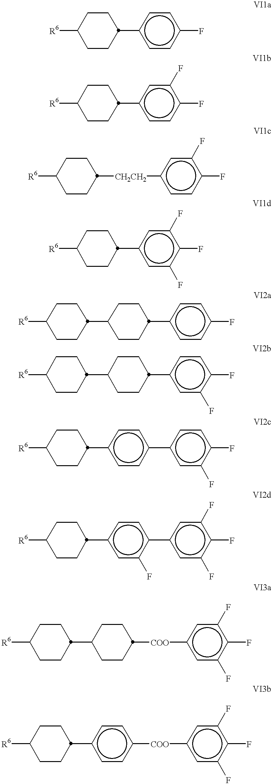
in which
R6 is as defined above under the formula VI.
The liquid-crystal media employed in accordance with the invention preferably comprise from 40% to 75% of one or more, preferably more, preferably highly dielectrically positive compound(s) selected from the group consisting of the compounds of the formulae I and II, preferably from the group consisting of the compounds of the formulae I1 and II2.
In a preferred embodiment, the liquid-crystal media employed in accordance with the invention comprise in total, based on the mixture as a whole,
from 40% to 70% of compounds of the formula I
from 0% to 30% of compounds of the formula II, and
from 0% to 40% of compounds of the formula III.
Here, as in the entire present application, the term “compounds”, for clarification also written as compound(s), is taken to mean, unless expressly stated otherwise, both one compound and a plurality of compounds.
The individual compounds of Formulas I to VI here are generally employed in concentrations of from 1% to 30%, preferably from 2% to 20% and particularly preferably from 4% to 16%.
In a particularly preferred embodiment, the compounds of the various formulae are employed in the liquid-crystal media employed in accordance with the invention as summarized in the following table.
| Formulae | Ranges |
| gen. | preferably | generally | preferably | part. pref. |
| I | I1 | 42% to 65% | 45% to 60% | 45% to 58% |
| II | II3 | 0% to 25% | 0% to 20% | 5% to 20% |
| III | III1a-II1c, III2c, | 0% to 36% | 0% to 30% | 2% to 20% |
| III3a, III3b and | ||||
| III3d | ||||
| IV | IV1a, V2a and | 0% to 20% | 5% to 15% | 7% to 14% |
| IV3b | ||||
| V | V1a | 0% to 20% | 0% to 15% | 0% to 10% |
| VI | VI1, VI2c and | 0% to 40% | 2% to 30% | 3% to 25% |
| VI3a | ||||
The liquid-crystal media in this embodiment very particular preferably comprise in total
from 50% to 58% of compounds of the formula I,
from 7% to 16% of compounds of the formula II,
from 2% to 20% of compounds of the formula III,
from 7% to 14% of compounds of the formula IV,
from 0% to10% of compounds of the formula V, and
from 10% to 25% of compounds of the formula VI.
In a particularly preferred embodiment, which may be identical and preferably is identical with the preferred embodiments described above for the preferred concentrations ranges, the liquid-crystal media comprise
one or more compounds of the formula I1 and/or
one or more compounds of the formula II3 and/or
one or more compounds selected from the group consisting of the compounds of the formula III1a to III1c and/or
one or more compounds selected from the group consisting of the compounds of the formulae III2 to III3 and/or
one or more compounds selected from the group consisting of the compounds of the formulae VI1d, VI2b, VI2c, VI3a and VI3b.
Particular preference is given here to liquid-crystal media which satisfy one or more of the following conditions. The media comprise
one or more compounds of the formula I1, in particular in each case in concentrations of from 3% to 15% per compound,
one or more compounds of the formula II3, in particular in each case in concentrations of from 5% to 20% per compound,
one or more compounds of the formula III1, in particular in each case in concentrations of from 3% to 15% per compound,
one or more compounds of the formula III2, in particular in each case in concentrations of from 3% to 12% per compound, preferably in each case at least one compound in which R31 is alkenyl,
one or more compounds of the formulae III1a and/or III1c, in particular in concentrations of from 4% to 15% per compound,
one or more compounds of the formula III2a,
one or more compound(s) of the formula VI2b and/or of the formula VI3a.
The above-mentioned preferred concentration ranges particularly preferably also apply to this preferred combination of compounds.
The liquid-crystal media used in accordance with the invention preferably have nematic phases of in each case at least from −20° C. to 70° C., preferably from −30° C. to 80° C. and very particularly preferably from −40° C. to 80° C. The term “have a nematic phase” here means firstly that no smectic phase and no crystallization are observed at low temperatures at the corresponding temperature and secondly that no clearing occurs on heating from the nematic phase. The investigation at low temperatures is carried out in a flow viscometer at the corresponding temperature and checked by storage in test cells having a layer thickness corresponding to the electro-optical application for at least 100 hours. At high temperatures, the clearing point is measured by conventional methods in capillaries.
Furthermore, the liquid-crystal media used in accordance with the invention are characterized by optical anisotropy values which are particularly suitable for STN displays having conventional layer thicknesses. The birefringence values are in the range from 0.100 to 0.180, preferably in the range from 0.120 to 0.170 and very particularly preferably in the range from 0.120 to 0.160 and most preferably in the range from 0.130 to 0.150.
In addition, the liquid-crystal displays according to the invention have relatively low threshold voltage values of less than or equal to 1.8 V, preferably less than or equal to 1.7 V, particularly preferably less than or equal to 1.5 V and very particularly preferably less than or equal to 1.0 V.
The steepness values of the electro-optical-characteristic line of the liquid-crystal displays are preferably less than or equal to 1.100, particularly preferably less than or equal to 1.080, very particularly preferably less than or equal to 1.060 and in particular less than or equal to 1.040. They are generally at values of 1.020 or greater.
The use of alignment layers of low layer thickness improves the steepness of the electro-optical characteristic line of the displays. The difference in the steepness of the characteristic line from 1 (V90/V10−1) of the displays according to the invention is preferably less than 80% of the corresponding value of an otherwise identical display having alignment layers with a layer thickness of 100 nm. This value is particularly preferably less than 70% and very particularly preferably at most 50% of the comparative value of the comparative display having an alignment layer with a thickness of 100 nm. Particular preference is given to liquid-crystal displays in which the difference of the steepness values from 1 is 90% or less, preferably 75% or less and particularly preferably 50% or less than the corresponding value of a comparative display having a layer thickness of the alignment layer of 70 nm.
The alignment layer preferably has a refractive index in the range from 1.550 to 1.800, particularly preferably in the range from 1.590 to 1.750 and very particularly preferably in the range from 1.600 to 1.700.
The transmission by the alignment layer (where twice the layer thickness is taken into account since both substrates of the display carry an alignment layer) at a wavelength of 390 nm is preferably 90% or more, particularly preferably 95% or more, very particularly preferably 97% or more and in particular 99% or more.
The various preferred ranges for the values of the individual physical properties of the alignment layer and of the liquid-crystal material are preferably also observed both with one another and combined amongst one another. Thus, for example, the liquid-crystal media according to the invention have, in particular, the following property combinations:
| Phase: T/ | V10(240°/ | ||
| Embodiment | ° C. | Δn | 5°/V |
| Preferred | ≦ −20 to ≧ 80 | 0.12 ≦ to ≦ 0.18 | ≦2.0 |
| Particularly preferred | ≦ −30 to ≧ 90 | 0.13 ≦ to ≦ 0.17 | ≦1.9 |
| Especialy preferred | ≦ −40 to ≧ 100 | 0.14 ≦ to ≦ 0.07 | ≦1.8 |
| where here, as in the entire application, “≦” means less than or equal to, and “≧” means greater than or equal to. | |||
The twist angle of the liquid-crystal layer of the liquid-crystal displays according to the invention is preferably from 180° C. to 290° C., particularly preferably from 180° to 270°, very particular preferably from 180° to 260° and especially preferably from 200° to 245°.
The surface tilt angle is preferably in the range from 20° to 25°, particularly preferably in the range from 3° to 15°, very particularly preferably in the range from 3° to 9° and in particular in the range from 4° to 7°.
The layer thickness of the liquid-crystal layer of the displays according to the invention is preferably from 3μm to 8 μm, particular preferably from 4 μm to 6.5 μm.
The term “alkyl” preferably covers straight-chain and branched alkyl groups having 1-7 carbon atoms, in particular the straight-chain groups methyl, ethyl, propyl, butyl, pentyl, hexyl and heptyl. Groups having 2-5 carbon atoms are generally preferred.
The term “alkenyl” preferably covers straight-chain and branched alkenyl groups having 2-7 carbon atoms, in particular the straight-chain groups. Particularly preferred alkenyl groups are C2-C7-1E-alkenyl, C4-C7-3E-alkenyl, C5-C7-4-alkenyl, C6-C7-5-alkenyl and C7-6-alkenyl, in particular C2-C7-1E-alkenyl, C4-C7-3E-alkenyl and C5-C7-4-alkenyl. Examples of further preferred alkenyl groups are vinyl, 1E-propenyl, 1E-butenyl, 1E-pentenyl, 1E-hexenyl, 1E-heptenyl, 3-butenyl, 3E-pentenyl, 3E-hexenyl, 3E-heptenyl, 4-pentenyl, 4Z-hexenyl, 4E-hexenyl, 4Z-heptenyl, 5-hexenyl, 6-heptenyl and the like. Groups having up to 5 carbon atoms are generally preferred.
The term “oxaalkyl” or alkoxyalkyl preferably covers straight-chain radicals of the formula CnH2n+1—O—(CH2)m, in which n and m are each, independently of one another, from 1 to 6, and the sum of m+n is up to 7. Preferably, n=1 and m is from 1 to 6.
Through a suitable choice of the meanings of the parameters of the compounds, in particular of R1, Y1, R2, Y21, Y22 but also the parameters of the other compounds, the addressing times, the threshold voltage, the steepness of the transmission characteristic lines, etc., can be modified in the desired manner. For example, 1E-alkenyl radicals, 3E-alkenyl radicals, 2E-alkenyloxy radicals and the like generally result in shorter addressing times, improved nematic tendencies and a higher ratio of the elastic constants k33 (bend) and k11 (splay) compared with alkyl or alkoxy radicals. 4-alkenyl radicals, 3-alkenyl radicals and the like generally give lower threshold voltages and smaller values of k33/k11 compared with alkyl and alkoxy radicals.
A —CH2CH2— group generally results in higher values of k33/k11 compared with the single covalent bond. Higher values of k33/k11 facilitate, for example, flatter transmission characteristic lines in TN cells with a 90° twist (for achieving grey shades) and steeper transmission characteristic lines in STN, SBE and OMI cells (greater multiplexability), and vice versa.
In the present application, the term “dielectrically very highly positive compounds” denotes compounds having a Δ∈ of >20, the term “dielectrically highly positive compounds” denotes compounds having a Δ∈ in the range from less than 20 to Δ∈=10, the term “dielectrically slightly positive compounds” denotes compounds having a Δ∈ in the range from less than 10 to Δ∈>1.5, the term “dielectrically neutral compounds” denotes those in which −1.5≦Δ∈≦1.5, and the term “dielectrically negative compounds” denotes those in which Δ∈ is <−1.5. The dielectric anisotropy of the compounds is determined here by dissolving 10% of the compounds in a liquid-crystalline host and determining the capacitance of this mixture in at least one test cell in each case with a thickness of 10 μm with homeotropic and with homogeneous surface alignment at 1 kHz. The measurement voltage is typically from 0.2 V to 1.0 V, but is always less than the capacitive threshold of the respective liquid-crystal mixture.
The host mixture used for dielectrically positive compounds is ZLI-4792, and the host mixture used for dielectrically neutral and dielectrically negative compounds is ZLI-3086, both from Merck KGaA, Germany. The values for the respective compounds to be investigated are obtained from the change in the dielectric constants of the host mixture after addition of the compound to be investigated and extrapolation to 100% of the compound employed.
The term “threshold voltage” usually relates to the optical threshold for 10% relative contrast (V10).
All concentrations in this application, unless explicitly stated otherwise, are given in per cent by weight and relate to the corresponding mixture as a whole. All physical properties are and were determined in accordance with “Merck Liquid Crystals, Physical Properties of Liquid Crystals”, as of Nov. 1997, Merck KGaA, Germany, and apply for a temperature of 20° C., unless explicitly stated otherwise. Δn is determined at 589 nm and Δ∈ at 1 kHz.
The threshold voltages and the other electro-optical properties were determined in test cells manufactured at Merck KGaA, Germany, using white light and using a commercial Autronic-Melchers DMS-301 measuring instrument. To this end, cells were selected, depending on Δn of the liquid crystals, having a thickness corresponding to an optical retardation d·Δn of the cells of about 0.85 μm. The cells had a twist angle of 240°. The d/P value was set at 0.53 by means of the chiral dopant S-811 (Merck KGaA, Darmstadt, Germany). The cells were operated in so-called “yellow mode”. For the standard characterization of the electro-optical properties of the liquid-crystal mixtures, in particular of the characteristic voltages, such as the threshold voltage, cells containing SE 4110 from Nissan Chemicals, Japan, with a layer thickness of the polyimide of about 30 nm as alignment layer were used. The characteristic voltages were all determined with perpendicular observation. The threshold voltage was indicated as V10 for 10% relative contrast, the mid-grey voltage V═, was indicated for 50% relative contrast and the saturation voltage V90 was indicated for 90% relative contrast.
In the case of some liquid-crystal media, the threshold voltage was additionally determined as the capacitive threshold V0 (also known as the Freedericks threshold).
The liquid-crystal media according to the invention may, if desired, also comprise furthermore additives in the conventional amounts. The amount of these additives employed, like that of the chiral dopants, is in total from 0% to 10%, based on the amount of the mixture as a whole, preferably from 0.1% to 6%. The concentration of the individual compounds employed is preferably from 0.1 to 3%. The concentration of these and similar additives is not taken into account when specifying the concentrations and the concentration ranges of the liquid-crystal compounds in the liquid-crystal media.
The liquid-crystal media employed in accordance with the invention consist of a plurality of compounds, preferably from 3 to 30, particularly preferably from 6 to 20 and very particularly preferably from 10 to 16 compounds, which are mixed in a conventional manner. In general, the desired amount of the components used in lesser amount are dissolved in the components making up the principal constituent, advantageously at elevated temperature. If the selected temperature is above the clearing point of the principal constituent, the completeness of the dissolution process is particularly easy to observe. However, it is also possible to prepare the liquid-crystal mixtures by other conventional methods, for example using premixtures or from a so-called “multibottle system”. By means of suitable additives, the liquid-crystal phases employed in accordance with the invention can be modified in such a way that they can be employed in any type of STN display that has been disclosed hitherto.
The entire disclosure of all applications, patents and publications, cited above and below, and of corresponding German Application No. 100 188 882.6, filed Apr. 14, 2000 is hereby incorporated by reference.
The examples below serve to illustrate the invention without representing a limitation. In the examples, the melting point T (C,N), the transition from the smectic (S) to the nematic (N) phase T(S,N) and the clearing point T (N,I) of a liquid-crystal substance are given in degrees Celsius. The percentages are, unless explicitly stated otherwise, per cent by weight above and below, and the physical properties are the values at 20° C., unless explicitly stated otherwise.
All temperature values indicated in this application are° C. and all temperature differences are correspondingly differential degrees, unless explicitly stated otherwise.
In the present application and in the following examples, the structures of the liquid-crystal compounds are indicated by means of acronyms, the transformation into chemical formulae taking place in accordance with Tables A and B below. All radicals CnH2n+1 and CmH2m+1 are straight-chain alkyl radicals having n and m carbon atoms respectively. The coding in Table B is self-evident. In Table A, only the acronym for the parent structure is given. In individual cases, the acronym for the parent structure is followed, separated by a dash, by a code for the substituents R1, R2, L1 and L2:
| Code for R1, | ||||
| R2, L1, L2 | R1 | R2 | L1 | L2 |
| nm | CnH2n+1 | CmH2m+1 | H | H |
| nOm | CnH2n+1 | OcmH2m+1 | H | H |
| nO.m | OcnH2n+1 | CmH2m+1 | H | H |
| n | CnH2n+1 | CN | H | H |
| nN.F | CnH2n+1 | CN | H | F |
| nN.F.F | CnH2n+1 | CN | F | F |
| nF | CnH2n+1 | F | H | H |
| nF.F | CnH2n+1 | F | H | F |
| nF.F.F | CnH2n+1 | F | F | F |
| nOF | OcnH2n+1 | F | H | H |
| nCl | CnH2n+1 | Cl | H | H |
| nCl.F | CnH2n+1 | Cl | H | F |
| nCl.F.F | CnH2n+1 | Cl | F | F |
| nmF | CnH2n+1 | CmH2m+1 | F | H |
| nCF3 | CnH2n+1 | CF3 | H | H |
| nOCF3 | CnH2n+1 | OCF3 | H | H |
| nOCF3.F | CnH2n+1 | OCF3 | H | F |
| nOCF3.F.F | CnH2n+1 | OCF3 | F | F |
| nOCF2 | CnH2n+1 | OCHF2 | H | H |
| nOCF2.F | CnH2n+1 | OCHF2 | H | F |
| nOCF2.F.F | CnH2n+1 | OCHF2 | F | F |
| nS | CnH2n+1 | NCS | H | H |
| nVsN | CrH2r+1—CH=CH—CsH2s—- | CN | H | H |
| nEsN | CrH2r+1—O—CsH2s— | CN | H | H |
| nAm | CnH2n+1 | COOCmH2m+1 | H | H |
| TABLE A |
 |
| PYP |
 |
| PYRP |
 |
| BCH |
 |
| CBC |
 |
| CCH |
 |
| CCP |
 |
| CP |
 |
| CPTP |
 |
| CEPTP |
 |
| D |
 |
| ECCP |
 |
| CECP |
 |
| EPCH |
 |
| HP |
 |
| ME |
 |
| PCH |
 |
| PDX |
 |
| PTP |
 |
| BECH |
 |
| EBCH |
 |
| CPC |
 |
| EHP |
 |
| BEP |
 |
| ET |
| TABLE B |
 |
| CCZU-n-X |
 |
| CDU-n-X |
 |
| T15 |
 |
| K3.n |
 |
| M3.n |
 |
| CGP-n-X |
 |
| Inm |
 |
| CGU-n-X |
 |
| C-nm |
 |
| C15 |
 |
| CB15 |
 |
| CBC-nm(F) |
 |
| CCN-nm |
 |
| G3.n |
 |
| CCEPC-nm |
 |
| CCPC-nm |
 |
| CH-nm |
 |
| HD-nm |
 |
| HH-nm |
 |
| NCB-nm |
 |
| OS-nm |
 |
| CHE |
 |
| ECBC-nm |
 |
| ECCH-nm |
 |
| CCH-n1Em |
 |
| T-nFN |
 |
| B-nO.FN |
 |
| CVCC-n-m |
 |
| CVCP-n-m |
 |
| CVCVC-n-m |
 |
| CP-V-N |
 |
| CC-n-V |
 |
| CCG-V-F |
 |
| CPP-nV2-m |
 |
| CCP-V-m |
 |
| CCP-V2-m |
 |
| CPP-V-m |
 |
| CPP-nV-m |
 |
| CPP-Vn-m |
 |
| CC-V-V |
 |
| CC-nV-V |
 |
| CC-nV-Vm |
 |
| CC-Vn-V |
 |
| CC-Vn-mV |
 |
| PCH-n(O)mFF |
 |
| CCP-n(O)mFF |
 |
| CP-V-N |
 |
| CP-nV-N |
 |
| CP-Vn-N |
 |
| CP-nVm-N |
The following examples explain the present invention without restricting it in any way. However, they reproduce typical favorable embodiments. From the disclosure content of the examples, further objects of the present invention are evident to the person skilled in the art. In particular, preferred values for the physical properties and their combinations are evident, both for the displays and for the materials used.
A liquid-crystal mixture M 1 was prepared. The composition and physical properties of this mixture are shown in the following table (Table 1).
| TABLE 1 |
| Composition and properties of mixture M 1 |
| Compound/ | Concentration/ | |
| abbreviation | % | Physical properties |
| PCH-3N.F.F | 7.0 | Clearing point: T(N, I) = 82.5° C. |
| ME2N.F | 10.0 | ne (20° C., 589 nm) = 1.6385 |
| ME3N.F | 10.0 | Δn (20° C., 589 nm) = 0.1420 |
| ME4N.F | 14.0 | εII (20° C., 1 kHz) = 62.6 |
| ME5N.F | 14.0 | Δε (20° C., 1 kHz) = 51.1 |
| HP-3N.F | 6.0 | |
| HP-4N.F | 5.0 | HTPS-811 (20° C.) = −13.96 m−1 |
| HP-5N.F | 5.0 | |
| CCZU-2-F | 5.0 | φ = 240° |
| CCZU-3-F | 9.0 | V10 (20° C.) = 0.77 V |
| CCZU-5-F | 5.0 | |
| CCPC-33 | 5.0 | |
| CCPC-34 | 5.0 | |
| Σ | 100.0 | |
The liquid-crystal medium was investigated in test cells with various alignment layers. The alignment layer used for this investigation was the polyimide SE 3140 from Nissan Chemicals, Japan.
For a given polyimide, the layer thickness of the polyimide layer (d(PI)) was varied systematically. It was ensured here that no pinholes occurred, even in the case of the relatively small layer thicknesses.
For the polyimide SE 3140, cells having polyimide layer thicknesses of 15, 30, 50 and 70 nm were investigated. The results for the characteristic voltages are shown in the following table (Table 2).
| TABLE 2 |
| Characteristic voltages of STN cells containing SE 3140 and |
| liquid-crystal mixture M 1 |
| d(Pl)/nm | V10/V | V90/V | V90/V10 | ||
| 70 | 0.829 | 0.953 | 1.150 | ||
| 50 | 0.788 | 0.895 | 1.135 | ||
| 30 | 0.776 | 0.858 | 1.106 | ||
| 15 | 0.754 | 0.802 | 1.063 | ||
A liquid-crystal mixture M 2 was prepared. The composition and physical properties of this mixture are shown in the following table (Table 3).
| TABLE 3 |
| Composition and properties of mixture M 2 |
| Compound/ | Concentration/ | |
| abbreviation | % | Physical properties |
| PCH-3N.F.F | 13.0 | Clearing point: T(N, I) = 86.5° C. |
| ME2N.F | 6.0 | ne (20° C., 589 nm) = 1.6386 |
| ME3N.F | 6.0 | Δn (20° C., 589 nm) = 0.1419 |
| ME4N.F | 10.0 | |
| ME5N.F | 9.0 | HTPS-811 (20° C.) = −12.43 m−1 |
| CC-S-V | 9.0 | |
| CCG-V-F | 22.0 | Φ = 240° |
| CCPC-33 | 3.0 | V10 (20° C.) = 1.15 V |
| CCPC-34 | 3.0 | |
| CBC-33F | 4.0 | |
| CPTP-301 | 5.0 | |
| CPTP-302 | 5.0 | |
| CPTP-303 | 5.0 | |
| Σ | 100.0 | |
As in Example 1, cells containing the polyimide SE 3140 with polyimide layer thicknesses of 15, 30, 50 and 70 nm were produced and investigated. The results for the characteristic voltages are shown in the following table (Table 4).
| TABLE 4 |
| Characteristic voltages of STN cells containing SE 3140 and |
| liquid-crystal mixture M 2 |
| d(Pl)/nm | V10/V | V90/V | V90/V10 | ||
| 70 | 1.188 | 1.315 | 1.107 | ||
| 50 | 1.176 | 1.286 | 1.094 | ||
| 30 | 1.158 | 1.244 | 1.074 | ||
| 15 | 1.154 | 1.218 | 1.055 | ||
In the following examples, test cells containing the alignment layer SE 3140 in layer thicknesses of 70, 50, 30 and 15 nm were produced as in Example 1 and filled with various liquid-crystal media and investigated.
| TABLE 5 |
| Composition and properties of mixture M 3 |
| Compound/ | Concentration/ | |
| Abbreviation | % | Physical properties |
| ME2N.F | 14.0 | Clearing point: (N, I) = 90.0° C. |
| ME3N.F | 14.0 | Transition (S, N) < −40° C. |
| ME4N.F | 13.0 | ne(20° C., 589 nm) = 1.6484 |
| ME5N.F | 13.0 | Δn (20° C., 589 nm) = 0.1493 |
| HP-3N.F | 5.0 | ν(20° C.) = 76 cSt |
| HP-4N.F | 5.0 | ν(0° C.) = 454 cSt |
| HP-5N.F | 5.0 | ν(−20° C.) = 7720 cSt |
| CCG-V-F | 13.0 | |
| CC-5-V | 6.0 | Φ = 240° |
| CCPC-33 | 4.0 | V10 (20° C.) = 0.82 V |
| CCPC-34 | 4.0 | |
| CCPC-35 | 4.0 | |
| Σ | 100.0 | |
| TABLE 6 |
| Composition and properties of mixture M 4 |
| Compound/ | Concentration/ | |
| Abbreviation | % | Physical properties |
| ME2N.F | 14.0 | Clearing point: (N, I) = 52.0° C. |
| ME3N.F | 14.0 | |
| ME4N.F | 13.0 | Δn (20° C., 589 nm) = 0.1448 |
| ME5N.F | 13.0 | |
| PYP-31 | 5.0 | |
| PYP-32 | 5.0 | |
| HP-3N.F | 5.0 | |
| HP-4N.F | 5.0 | |
| HP-5N.F | 5.0 | |
| CCG-V-F | 15.0 | |
| CC-5-V | 6.0 | |
| Σ | 100.0 | |
| TABLE 7 |
| Composition and properties of mixture M 5 |
| Compound/ | Concentration/ | |
| abbreviation | % | Physical properties |
| ME2N.F | 14.0 | Clearing point: (N, I) = 59.5° C. |
| ME3N.F | 14.0 | Transition (S, N) < −40° C. |
| ME4N.F | 13.0 | Δn (20° C., 589 nm) = 0.1537 |
| ME5N.F | 13.0 | ν(20° C.) = 69 cSt |
| PYP-31 | 6.0 | ν(0° C.) = 440 cSt |
| PYP-32 | 5.0 | ν(−20° C.) = 7070 cSt |
| HP-3N.F | 5.0 | |
| HP-4N.F | 5.0 | |
| HP-5N.F | 5.0 | |
| CCG-V-F | 17.0 | |
| CC-5-V | 3.0 | |
| Σ | 100.0 | |
| TABLE 8 |
| Composition and properties of mixture M 6 |
| Compound/ | Concentration/ | |
| Abbreviation | % by weight | Physical properties |
| ME2N.F | 14.0 | Clearing point (N,I) = 74.5° C. |
| ME3N.F | 14.0 | Δn (20° C., 589 nm) = 0.1593 |
| ME4N.F | 13.0 | |
| ME5N.F | 13.0 | |
| PYP-4 | 8.0 | |
| HP-3N.F | 5.0 | |
| HP-4N.F | 5.0 | |
| HP-5N.F | 5.0 | |
| CCG-V-F | 17.0 | |
| CCPC-33 | 3.0 | |
| CCPC-34 | 3.0 | |
| Σ | 100.0 | |
| TABLE 9 |
| Composition and properties of mixture M 7 |
| Compound/ | Concentration/ | |
| Abbreviation | % by weight | Physical properties |
| ME2N.F | 14.0 | Clearing point (N,I) = 73.0° C. |
| ME3N.F | 14.0 | Δn (20° C., 589 nm) = 0.1658 |
| ME4N.F | 13.0 | |
| ME5N.F | 13.0 | |
| PYP-4 | 12.0 | |
| HP-3N.F | 5.0 | |
| HP-4N.F | 5.0 | |
| HP-5N.F | 5.0 | |
| CCG-V-F | 13.0 | |
| CCPC-33 | 3.0 | |
| CCPC-34 | 3.0 | |
| Σ | 100.0 | |
| TABLE 10 |
| Composition and properties of mixture M 8 |
| Compound/ | Concentration/ | |
| Abbreviation | % by weight | Physical properties |
| ME2N.F | 14.0 | Clearing point (N,I) = 70.0° C. |
| ME3N.F | 14.0 | Transition (S,N) < −40° C. |
| ME4N.F | 13.0 | Δn (20° C., 589 nm) = 0.1537 |
| ME5N.F | 13.0 | ν(20° C.) = 96 cSt |
| PYP-4 | 11.0 | ν(0° C.) = 700 cSt |
| HP-4N.F | 5.0 | ν(−20° C.) = 14760 cSt |
| HP-5N.F | 5.0 | |
| CCZU-2-F | 8.0 | Φ = 90° |
| CCZU-3-F | 11.0 | V10 (20° C.) = 0.61 V |
| CCPC-33 | 4.0 | |
| CCPC-34 | 4.0 | |
| Σ | 100.0 | |
| TABLE 11 |
| Composition and properties of mixture M 9 |
| Compound/ | Concentration/ | |
| Abbreviation | % by weight | Physical properties |
| ME2N.F | 14.0 | Clearing point (N,I) = 83.0° C. |
| ME3N.F | 14.0 | ne (20° C., 589 nm) = 1.6876 |
| ME4N.F | 15.0 | Δn (20° C., 589 nm) = 0.1813 |
| ME5N.F | 15.0 | |
| HP-3N.F | 5.0 | Φ = 90° |
| HP-4N.F | 5.5 | V10 (20° C.) = 0.64 V |
| HP-5N.F | 5.5 | |
| CCG-V-F | 12.0 | |
| CPTP-301 | 5.0 | |
| CPTP-302 | 5.0 | |
| CPTP-303 | 4.0 | |
| Σ | 100.0 | |
| TABLE 12 |
| Composition and properties of mixture M 10 |
| Compound/ | Concentration/ | |
| Abbreviation | % by weight | Physical properties |
| ME2N.F | 14.0 | Clearing point (N,I) = 77.5° C. |
| ME3N.F | 14.0 | ne (20° C., 589 nm) = 1.6798 |
| ME4N.F | 15.0 | Δn (20° C., 589 nm) = 0.1739 |
| ME5N.F | 15.0 | |
| HP-3N.F | 5.0 | Φ = 90° |
| HP-4N.F | 5.0 | V10 (20° C.) = 0.63 V |
| HP-5N.F | 5.0 | |
| CCG-V-F | 15.5 | |
| CPTP-301 | 3.5 | |
| CPTP-302 | 4.0 | |
| CPTP-303 | 4.0 | |
| Σ | 100.0 | |
| TABLE 13 |
| Composition and properties of mixture M 11 |
| Compound/ | Concentration/ | |
| Abbreviation | % by weight | Physical properties |
| ME2N.F | 14.0 | Clearing point (N,I) = 89.0° C. |
| ME3N.F | 14.0 | Transition (S,N) < −40° C. |
| ME4N.F | 14.5 | ne (20° C., 589 nm) = 1.6623 |
| ME5N.F | 14.5 | Δn (20° C., 589 nm) = 0.1601 |
| HP-3N.F | 5.0 | Δε (20° C., 1 kHz) = 57.7 |
| HP-4N.F | 5.0 | ν(20° C.) = 95 cSt |
| HP-5N.F | 5.0 | ν(0° C.) = 630 cSt |
| CCG-V-F | 15.5 | ν(−20° C.) = 12800 cSt |
| CPTP-302 | 2.5 | |
| CCPC-33 | 4.0 | Φ = 90° |
| CCPC-34 | 3.0 | V10 (20° C.) = 0.63 V |
| CCPC-35 | 3.0 | |
| Σ | 100.0 | |
| TABLE 14 |
| Composition and properties of mixture M 12 |
| Compound/ | Concentration/ | |
| Abbreviation | % by weight | Physical properties |
| ME2N.F | 12.0 | Clearing point (N,I) = 60.5° C. |
| ME3N.F | 12.0 | Transition (S,N) < −40° C. |
| ME4N.F | 12.0 | ne (20° C., 589 nm) = 1.6463 |
| ME5N.F | 12.0 | Δn (20° C., 589 nm) = 0.1462 |
| PYP-4 | 10.0 | Δε (20° C., 1 kHz) = 57.7 |
| HP-3N.F | 5.0 | ν(20° C.) = 76 cSt |
| HP-4N.F | 5.0 | ν(0° C.) = 440 cSt |
| HP-5N.F | 5.0 | ν(−20° C.) = 6800 cSt |
| CC-5-V | 8.0 | |
| CCZU-2-F | 8.0 | Φ = 90° |
| CCZU-3-F | 11.0 | V10 (20° C.) = 0.66 V |
| Σ | 100.0 | |
| TABLE 15 |
| Composition and properties of mixture M 13 |
| Compound/ | Concentration/ | |
| Abbreviation | % by weight | Physical properties |
| ME2N.F | 13.0 | Clearing point (N,I) = 74.5° C. |
| ME3N.F | 13.0 | ne (20° C., 589 nm) = 1.6903 |
| ME4N.F | 15.0 | Δn (20° C.,589 nm) = 0.1826 |
| ME5N.F | 15.0 | |
| HP-3N.F | 5.0 | Φ = 90° |
| HP-4N.F | 5.0 | V10 (20° C.) = 0.65 V |
| HP-5N.F | 6.0 | |
| CCG-V-F | 16.5 | |
| PPTUI-3-2 | 11.5 | |
| Σ | 100.0 | |
| TABLE 16 |
| Composition and properties of mixture M 14 |
| Compound/ | Concentration/ | |
| Abbreviation | % by weight | Physical properties |
| ME2N.F | 14.0 | Clearing point (N,I) = 72.0° C. |
| ME3N.F | 14.0 | ne (20° C., 589 nm) = 1.6913 |
| ME4N.F | 15.0 | Δn (20° C., 589 nm) = 0.1819 |
| ME5N.F | 15.0 | |
| HP-3N.F | 5.0 | Φ = 90° |
| HP-4N.F | 5.0 | V10 (20° C.) = 0.65 V |
| HP-5N.F | 5.0 | |
| BCH-3F.F | 2.0 | |
| BCH-5F.F | 7.0 | |
| CCG-V-F | 3.0 | |
| CCP-V-1 | 6.0 | |
| PPTUI-3-2 | 9.0 | |
| Σ | 100.0 | |
| TABLE 17 |
| Composition and properties of mixture M 15 |
| Compound/ | Concentration/ | |
| Abbreviation | % by weight | Physical properties |
| ME2N.F | 10.0 | Clearing point (N,I) = 103.5° C. |
| ME3N.F | 10.0 | ne (20° C., 589 nm) = 1.6767 |
| ME4N.F | 12.0 | Δn (20° C., 589 nm) = 0.1728 |
| ME5N.F | 12.0 | |
| CCG-V-F | 19.0 | Φ = 240° |
| CCP-V-1 | 8.0 | V10 (20° C.) = 1.10 V |
| PTP-102 | 5.0 | |
| CPTP-301 | 5.0 | |
| CPTP-302 | 5.0 | |
| CPTP-303 | 5.0 | |
| CCPC-33 | 5.0 | |
| CCPC-34 | 4.0 | |
| Σ | 100.0 | |
| TABLE 18 |
| Composition and properties of mixture M 16 |
| Compound/ | Concentration/ | |
| Abbreviation | % by weight | Physical properties |
| ME2N.F | 10.0 | Clearing point (N, I) = 108.0° C. |
| ME3N.F | 10.0 | ne (20° C., 589 nm) = 1.6435 |
| ME4N.F | 13.0 | Δn (20° C., 589 nm) = 0.1436 |
| ME5N.F | 13.0 | |
| CCG-V-F | 22.0 | Φ = 240° |
| CCP-V-1 | 10.0 | V10 (20° C.) = 1.10 V |
| CPTP-302 | 3.0 | |
| CBC-33F | 4.0 | |
| CCPC-33 | 5.0 | |
| CCPC-34 | 5.0 | |
| CCPC-35 | 5.0 | |
| Σ | 100.0 | |
| TABLE 19 |
| Composition and properties of mixture M 17 |
| Compound/ | Concentration/ | |
| Abbreviation | % by weight | Physical properties |
| ME2N.F | 12.0 | Clearing point (N, I) = 103.0° C. |
| ME3N.F | 10.0 | ne (20° C., 589 nm) = 1.6435 |
| ME4N.F | 13.0 | Δn (20° C., 589 nm) = 0.1435 |
| ME5N.F | 10.0 | |
| PCH-3 | 8.0 | Φ = 240° |
| CCG-V-F | 10.0 | V10 (20° C.) = 1.12 V |
| CCP-V-1 | 6.0 | |
| CCP-V2-1 | 12.0 | |
| CPTP-302 | 1.0 | |
| CBC-33 | 3.0 | |
| CCPC-33 | 5.0 | |
| CCPC-34 | 5.0 | |
| CCPC-35 | 5.0 | |
| Σ | 100.0 | |
| TABLE 20 |
| Composition and properties of mixture M 18 |
| Compound/ | Concentration/ | |
| Abbreviation | % by weight | Physical properties |
| ME2N.F | 9.0 | Clearing point (N, I) = 94.5° C. |
| ME3N.F | 9.0 | Transition (S, N) < −40° C. |
| ME4N.F | 10.0 | ne (20° C., 589 nm) = 1.6260 |
| ME5N.F | 8.0 | Δn (20° C., 589 nm) = 0.1292 |
| PCH-3N.F.F | 10.0 | Δε (20° C., 1 kHz) = 29.3 |
| CC-5-V | 6.0 | ν (20° C.) = 38 cSt |
| CCG-V-F | 16.0 | ν (0° C.) = 160 cSt |
| CCP-V-1 | 11.0 | ν (−20° C.) = 1500 St |
| CPTP-301 | 2.0 | ν (−30° C.) = 8200 cSt |
| CBC-33 | 2.0 | k1 (20° C.) = 8.3 pN |
| CBC-33F | 2.0 | k3/k1 (20° C.) = 2.62 |
| CCPC-33 | 5.0 | |
| CCPC-34 | 5.0 | Φ = 240° |
| CCPC-35 | 5.0 | V10 (20° C.) = 1.15 V |
| Σ | 100.0 | |
| TABLE 21 |
| Composition and properties of mixture M 19 |
| Compound/ | Concentration/ | |
| Abbreviation | % by weight | Physical properties |
| ME2N.F | 9.0 | Clearing point (N, I) = 111.0° C. |
| ME3N.F | 9.0 | ne (20° C., 589 nm) = 1.6243 |
| ME4N.F | 10.0 | Δn (20° C., 589 nm) = 0.1292 |
| ME5N.F | 10 8.0 | |
| CCZU-2-F | 4.0 | Φ = 240° |
| CCZU-3-F | 9.0 | V10 (20° C.) = 1.12 V |
| CCZU-5-F | 4.0 | |
| CCG-V-F | 16.0 | |
| CCP-V-1 | 12.0 | |
| CPTP-301 | 2.0 | |
| CCPC-33 | 5.0 | |
| CCPC-34 | 5.0 | |
| CCPC-35 | 5.0 | |
| Σ | 100.0 | |
| TABLE 22 |
| Composition and properties of mixture M 20 |
| Compound/ | Concentration/ | |
| Abbreviation | % by weight | Physical properties |
| ME2N.F | 10.0 | Clearing point (N, I) = 94.5° C. |
| ME3N.F | 10.0 | Transition (S, N) < −40° C. |
| ME4N.F | 12.0 | ne (20° C., 589 nm) = 1.6501 |
| ME5N.F | 12.0 | Δn (20° C., 589 nm) = 0.1515 |
| PTP-102 | 3.0 | Δε (20° C., 1 kHz) = 30.1 |
| CC-5-V | 11.0 | ν (20° C.) = 39 cSt |
| CCG-V-F | 19.0 | ν (0° C.) = 165 cSt |
| CPTP-301 | 4.0 | ν (−20° C.) = 1630 St |
| CPTP-302 | 4.0 | ν (−30° C.) = 9100 cSt |
| CPTP-303 | 3.0 | k1 (20° C.) = 9.0 pN |
| CCPC-33 | 4.0 | k3/k1 (20° C.) = 2.39 |
| CCPC-34 | 4.0 | |
| CCPC-35 | 4.0 | Φ = 240° |
| Σ | 100.0 | V10 (20° C.) = 1.12 V |
| TABLE 23 |
| Composition and properties of mixture M 21 |
| Compound/ | Concentration/ | |
| Abbreviation | % by weight | Physical properties |
| ME2N.F | 10.0 | Clearing point (N, I) = 108.5° C. |
| ME3N.F | 10.0 | ne (20° C., 589 nm) = 1.6520 |
| ME4N.F | 12.0 | Δn (20° C., 589 nm) = 0.1521 |
| ME5N.F | 12.0 | |
| CC-5-V | 4.0 | Φ = 240° |
| CCG-V-F | 19.0 | V10 (20° C.) = 1.13 V |
| CCP-V-1 | 8.0 | |
| CPTP-301 | 4.0 | |
| CPTP-302 | 4.0 | |
| CPTP-303 | 3.0 | |
| CCPC-33 | 5.0 | |
| CCPC-34 | 5.0 | |
| CCPC-35 | 4.0 | |
| Σ | 100.0 | |
| TABLE 24 |
| Composition and properties of mixture M 22 |
| Compound/ | Concentration/ | |
| Abbreviation | % by weight | Physical properties |
| ME2N.F | 8.0 | Clearing point (N, I) = 94.5° C. |
| ME3N.F | 8.0 | ne (20° C., 589 nm) = 1.6439 |
| ME4N.F | 11.0 | Δn (20° C.,589nm) = 0.1448 |
| ME5N.F | 10.0 | |
| PCH-3 | 20.0 | Φ = 240° |
| CCG-V-F | 11.0 | V10 (20° C.) = 1.20 V |
| CCP-V-1 | 9.0 | |
| CPTP-302 | 2.0 | |
| D-302FF | 2.0 | |
| CBC-33 | 5.0 | |
| CBC-33F | 4.0 | |
| CCPC-34 | 5.0 | |
| CCPC-34 | 5.0 | |
| Σ | 100.0 | |
The preceding examples can be repeated with similar success by substituting the generically or specifically described reactants and/or operating conditions of this invention for those used in the preceding examples.
From the foregoing description, one skilled in the art can easily ascertain the essential characteristics of this invention and, without departing from the spirit and scope thereof, can make various changes and modifications of the invention to adapt it to various usages and conditions.
Claims (32)
1. An electro-optical liquid-crystal display comprising a layer of liquid-crystal medium between two substrates with organic alignment layers on inside surfaces of each of said substrates;
the liquid-crystal layer having a twist angle, from one substrate to the other, of 110°-360°;
the liquid-crystal layer having a surface tilt angle of 2°-20°; and
each of said organic alignment layers having a thickness of 3 nm-150 nm, and
wherein the difference from 1 of the steepness of the electric-optical characteristic line, represented by the formula V90/V10−1, is half or less of the corresponding value of an otherwise identical display in which the layer thicknesses of each of the alignment layers is 100 nm.
2. A display according to claim 1 , at least one of said alignment layers has a layer thickness of 4 nm-60 nm.
3. A display according to claim 1 , wherein the steepness of the electro-optical characteristic line V90/V10 is 1.06 or less.
4. A display according to claim 1 , wherein the threshold voltage (V10) of the display is 1.20 V or less.
5. A display according to claim 1 , wherein said liquid-crystal medium comprises one or more compound(s) of formula I 
wherein
R1 is alkyl having 1 to 7 carbon atoms, alkoxy having 1 to 7 carbon atoms, alkoxyalkyl having 2 to 7 carbon atoms, alkenyl having 2 to 7 carbon atoms or alkenyloxy having 2 to 7 carbon atoms, and
Y1 is H or F.
6. A display according to claim 1 , wherein said liquid crystal medium comprises at least one compound of formula II 
wherein
R2 is alkyl having 1 to 7 carbon atoms, alkoxy having 1 to 7 carbon atoms, alkoxyalkyl having 2 to 7 carbon atoms, alkenyl having 2 to 7 carbon atoms or alkenyloxy having 2 to 7 carbon atoms, and
Y21 and Y22 are each, independently, H or F.
7. A display according to claim 5 , wherein said liquid crystal medium comprises at least one compound of formula II 
wherein
R2 is alkyl having 1 to 7 carbon atoms, alkoxy having 1 to 7 carbon atoms, alkoxyalkyl having 2 to 7 carbon atoms, alkenyl having 2 to 7 carbon atoms or alkenyloxy having 2 to 7 carbon atoms, and
Y21 and Y22 are each, independently, H or F.
8. A display according to claim 5 , wherein said liquid crystal medium comprises at least one compound of formula III 
wherein
R31 and R32 are each, independently of one another, alkyl having 1 to 7 carbon atoms, alkoxy having 1 to 7 carbon atoms, alkoxyalkyl, having 2 to 7 carbon atoms, alkenyl having 2 to 7 carbon atoms, or alkenyloxy having 2 to 7 carbon atoms, and
Z31, Z32 and Z33 are each, independently of one another, —CH2CH2—, —CH═CH—, —COO— or a single bond, 
o and p, independently of one another, are 0 or 1.
9. A display according to claim 6 , wherein said liquid crystal medium comprises at least one compound of formula III 
wherein
R31 and R32 are each, independently of one another, alkyl having 1 to 7 carbon atoms, alkoxy having 1 to 7 carbon atoms, alkoxyalkyl, having 2 to 7 carbon atoms, alkenyl having 2 to 7 carbon atoms, or alkenyloxy having 2 to 7 carbon atoms, and
Z31, Z32 and Z33 are each, independently of one another, —CH2CH2—, —CH═CH—, —COO— or a single bond, 
o and p, independently of one another, are 0 or 1.
10. A display according to claim 7 , wherein said liquid crystal medium comprises at least one compound of formula III 
wherein
R31 and R32 are each, independently of one another, alkyl having 1 to 7 carbon atoms, alkoxy having 1 to 7 carbon atoms, alkoxyalkyl, having 2 to 7 carbon atoms, alkenyl having 2 to 7 carbon atoms, or alkenyloxy having 2 to 7 carbon atoms, and
Z31, Z32 and Z33 are each, independently of one another, —CH2CH2—, —CH═CH—, —COO— or a single bond, 
o and p, independently of one another, are 0 or 1.
11. In a method of displaying information using an electro-optical liquid-crystal display, the improvement wherein said display is one in accordance with claim 1 .
12. A display according to claim 1 , wherein said organic alignment layers are a polyamide layer.
13. A display according to claim 1 , wherein said alignment layers each have a layer thickness of 7 nm-80 nm.
14. A display according to claim 1 , wherein said alignment layers each have a layer thickness of 8 nm-60 nm.
15. A display according to claim 1 , wherein said alignment layers each have a layer thickness of 10 nm-25 nm.
16. A display according to claim 1 , wherein said display has a nematic phase range of at least −20° to 70°, a birefringence of 0.100 to 0.180, a threshold voltage of less than or equal to 1.8 V, and a steepness value of the electro-optical characteristic line of less than or equal to 1.100.
17. A display according to claim 1 , wherein said alignment layers each have a refractive index of 1.550 to 1.800.
18. A display according to claim 1 , wherein said liquid-crystal layer having a surface tilt angle of 3°-150°.
19. An electro-optical liquid-crystal display comprising
a layer of liquid-crystal medium between two substrates with alignment layers on inside surfaces of each of said substrates;
the liquid-crystal layer having a twist angle, from one substrate to the other, of 110°-360°;
the liquid-crystal layer having a surface tilt angle of 2°-20°;
each of said alignment layers having a thickness of 3 nm-150 nm; and
at least one of said alignment layers is an organic layer, and
wherein the difference from 1 of the steepness of the electric-optical characteristic line, represented by the formula V90/V10−1, is half or less of the corresponding value of an otherwise identical display in which the layer thicknesses of each of the alignment layers is 100 nm.
20. A display according to claim 19 , at least one of said alignment layers has a layer thickness of 4 nm-60 nm.
21. In a method of displaying information using an electro-optical liquid-crystal display, the improvement wherein said display is one in accordance with claim 19 .
22. A display according to claim 19 , wherein the steepness of the electro-optical characteristic line V90/V10 is 1.06 or less.
23. A display according to claim 19 , wherein the threshold voltage (V10) of the display is 1.20 V or less.
24. A display according to claim 19 , wherein said organic alignment layers are a polyamide layer.
25. A display according to claim 19 , wherein said alignment layers each have a layer thickness of 7 nm-80 nm.
26. A display according to claim 19 , wherein said alignment layers each have a layer thickness of 8 nm-60 nm.
27. A display according to claim 19 , wherein said alignment layers each have a layer thickness of 10 nm-25 nm.
28. A display according to claim 19 , wherein said display has a nematic phase range of at least −20° to 70°, a birefringence of 0.100 to 0.180, a threshold voltage of less than or equal to 1.8 V, and a steepness value of the electro-optical characteristic line of less than or equal to 1.100.
29. A display according to claim 19 , wherein said alignment layers each have a refractive index of 1.550 to 1.800.
30. A display according to claim 19 , wherein said liquid-crystal layer having a surface tilt angle of 3°-15°.
31. In a method of displaying information using an electro-optical liquid-crystal display, the improvement wherein said display is one in accordance with claim 19 .
32. An electro-optical liquid-crystal display comprising
a layer of liquid-crystal medium between two substrates with alignment layers on inside surfaces of each of said substrates;
the liquid-crystal layer having a twist angle, from one substrate to the other, of 110°-360°;
the liquid-crystal layer having a surface tilt angle of 2°-20°; and
each of said alignment layers having a thickness of 3 nm-150 nm, and
wherein the difference from 1 of the steepness of the electric-optical characteristic line, represented by the formula V90/V10−1, is half or less of the corresponding value of an otherwise identical display in which the layer thicknesses of each of the alignment layers is 100 nm.
Applications Claiming Priority (3)
| Application Number | Priority Date | Filing Date | Title |
|---|---|---|---|
| DE10018882 | 2000-04-14 | ||
| DE10018882A DE10018882A1 (en) | 2000-04-14 | 2000-04-14 | Electrooptical liquid crystal displays, especially supertwisted nematic displays, have thin alignment layers and specified twist and surface tilt angles |
| DE10018882.6 | 2000-04-14 |
Publications (2)
| Publication Number | Publication Date |
|---|---|
| US20020086120A1 US20020086120A1 (en) | 2002-07-04 |
| US6800338B2 true US6800338B2 (en) | 2004-10-05 |
Family
ID=7638974
Family Applications (1)
| Application Number | Title | Priority Date | Filing Date |
|---|---|---|---|
| US09/834,762 Expired - Fee Related US6800338B2 (en) | 2000-04-14 | 2001-04-16 | Electro-optical liquid-crystal display |
Country Status (6)
| Country | Link |
|---|---|
| US (1) | US6800338B2 (en) |
| JP (1) | JP2001350145A (en) |
| KR (1) | KR20010103597A (en) |
| DE (2) | DE10018882A1 (en) |
| GB (1) | GB2366873B (en) |
| TW (1) | TW526257B (en) |
Cited By (5)
| Publication number | Priority date | Publication date | Assignee | Title |
|---|---|---|---|---|
| US20070003709A1 (en) * | 2005-06-29 | 2007-01-04 | Nano Loa, Inc. | Liquid crystal display device |
| US20070002267A1 (en) * | 2005-06-29 | 2007-01-04 | Nano Loa, Inc. | Liquid crystal display device |
| US20070145331A1 (en) * | 2005-12-22 | 2007-06-28 | Chisso Corporation | Liquid crystal composition and liquid crystal display device |
| US20070279541A1 (en) * | 2005-06-29 | 2007-12-06 | Nano Loa, Inc. | Method of driving liquid crystal display device |
| US20080246907A1 (en) * | 2007-04-04 | 2008-10-09 | Arima Display Corporation | Method for providing improved displaying effect of liquid crystal panel in operation temperature range thereof |
Families Citing this family (8)
| Publication number | Priority date | Publication date | Assignee | Title |
|---|---|---|---|---|
| JP4839524B2 (en) * | 2001-04-26 | 2011-12-21 | Dic株式会社 | Liquid crystal composition |
| DE10129335A1 (en) * | 2001-06-19 | 2003-01-02 | Merck Patent Gmbh | Polyimides with CF¶2¶O structural elements |
| US7271863B2 (en) * | 2002-10-16 | 2007-09-18 | Nitto Denko Corporation | Color liquid crystal display with internal rear polarizer |
| CN100453619C (en) * | 2002-12-11 | 2009-01-21 | 默克专利股份有限公司 | Fast switching liquid crystal compositions for use in bistable liquid crystal devices |
| US7294368B2 (en) * | 2002-12-11 | 2007-11-13 | Merck Patent Gmbh | Liquid crystal composition for use in bistable liquid crystal devices |
| CN100540631C (en) * | 2003-05-08 | 2009-09-16 | 默克专利股份有限公司 | The liquid-crystal composition that is used for bistable liquid crystal devices |
| JP2005156717A (en) * | 2003-11-21 | 2005-06-16 | Sony Corp | Liquid crystal display element and liquid crystal display device |
| CN105754098B (en) * | 2010-10-06 | 2018-05-18 | 株式会社日本显示器 | Composition for forming alignment film |
Citations (10)
| Publication number | Priority date | Publication date | Assignee | Title |
|---|---|---|---|---|
| US4974940A (en) * | 1988-05-07 | 1990-12-04 | Konica Corporation | Liquid crystal display device |
| DE4100276A1 (en) | 1990-01-05 | 1991-07-11 | Signode Corp | BINDING MACHINE, e.g. TAPE MACHINE |
| US5054889A (en) * | 1989-02-08 | 1991-10-08 | Yamaha Corp. | Liquid crystal display having an alignment layer in the form of a porous alumina layer |
| US5188758A (en) * | 1986-03-19 | 1993-02-23 | Merck Patent Gesellschaft Mit Beschraenkter Haftung | Electrooptical display element using a supertwist liquid crystal having specified elastic constants |
| US5520845A (en) * | 1993-12-02 | 1996-05-28 | E. I. Du Pont De Nemours And Company | Poly(2,6-piperazinedione) alignment layer for liquid crystal displays |
| US5578241A (en) * | 1993-05-18 | 1996-11-26 | Merck Patent Gesellschaft Mit Beschrankter Haftung | Liquid crystal display |
| EP0884625A2 (en) | 1997-06-13 | 1998-12-16 | Matsushita Electric Industrial Co., Ltd. | Liquid crystal display panel |
| US6016179A (en) | 1994-11-15 | 2000-01-18 | Sony Corporation | Liquid crystal display device |
| US6067139A (en) | 1997-06-26 | 2000-05-23 | E. I. Du Pont De Nemours And Company | Multi-domain STN LCD comprising fluorinated polyimide alignment layers |
| US6139926A (en) * | 1998-05-21 | 2000-10-31 | E. I. Du Pont De Nemours And Company | Polyimide photo alignment film from 3,3,4,4-benzophenone tetracarboxylic dianhydride and ortho-substituted aromatic diamines for liquid crystal displays |
Family Cites Families (1)
| Publication number | Priority date | Publication date | Assignee | Title |
|---|---|---|---|---|
| US6015179A (en) * | 1995-09-07 | 2000-01-18 | Weber; Walter | Device for mounting a hydraulically operated tailgate on a truck |
-
2000
- 2000-04-14 DE DE10018882A patent/DE10018882A1/en not_active Withdrawn
-
2001
- 2001-03-16 DE DE10112770A patent/DE10112770A1/en not_active Withdrawn
- 2001-04-03 GB GB0108361A patent/GB2366873B/en not_active Expired - Fee Related
- 2001-04-09 TW TW090108391A patent/TW526257B/en not_active IP Right Cessation
- 2001-04-14 KR KR1020010020017A patent/KR20010103597A/en not_active Application Discontinuation
- 2001-04-16 JP JP2001116755A patent/JP2001350145A/en active Pending
- 2001-04-16 US US09/834,762 patent/US6800338B2/en not_active Expired - Fee Related
Patent Citations (10)
| Publication number | Priority date | Publication date | Assignee | Title |
|---|---|---|---|---|
| US5188758A (en) * | 1986-03-19 | 1993-02-23 | Merck Patent Gesellschaft Mit Beschraenkter Haftung | Electrooptical display element using a supertwist liquid crystal having specified elastic constants |
| US4974940A (en) * | 1988-05-07 | 1990-12-04 | Konica Corporation | Liquid crystal display device |
| US5054889A (en) * | 1989-02-08 | 1991-10-08 | Yamaha Corp. | Liquid crystal display having an alignment layer in the form of a porous alumina layer |
| DE4100276A1 (en) | 1990-01-05 | 1991-07-11 | Signode Corp | BINDING MACHINE, e.g. TAPE MACHINE |
| US5578241A (en) * | 1993-05-18 | 1996-11-26 | Merck Patent Gesellschaft Mit Beschrankter Haftung | Liquid crystal display |
| US5520845A (en) * | 1993-12-02 | 1996-05-28 | E. I. Du Pont De Nemours And Company | Poly(2,6-piperazinedione) alignment layer for liquid crystal displays |
| US6016179A (en) | 1994-11-15 | 2000-01-18 | Sony Corporation | Liquid crystal display device |
| EP0884625A2 (en) | 1997-06-13 | 1998-12-16 | Matsushita Electric Industrial Co., Ltd. | Liquid crystal display panel |
| US6067139A (en) | 1997-06-26 | 2000-05-23 | E. I. Du Pont De Nemours And Company | Multi-domain STN LCD comprising fluorinated polyimide alignment layers |
| US6139926A (en) * | 1998-05-21 | 2000-10-31 | E. I. Du Pont De Nemours And Company | Polyimide photo alignment film from 3,3,4,4-benzophenone tetracarboxylic dianhydride and ortho-substituted aromatic diamines for liquid crystal displays |
Cited By (6)
| Publication number | Priority date | Publication date | Assignee | Title |
|---|---|---|---|---|
| US20070003709A1 (en) * | 2005-06-29 | 2007-01-04 | Nano Loa, Inc. | Liquid crystal display device |
| US20070002267A1 (en) * | 2005-06-29 | 2007-01-04 | Nano Loa, Inc. | Liquid crystal display device |
| US20070279541A1 (en) * | 2005-06-29 | 2007-12-06 | Nano Loa, Inc. | Method of driving liquid crystal display device |
| US20070145331A1 (en) * | 2005-12-22 | 2007-06-28 | Chisso Corporation | Liquid crystal composition and liquid crystal display device |
| US7452576B2 (en) * | 2005-12-22 | 2008-11-18 | Chisso Corporation | Liquid crystal composition and liquid crystal display device |
| US20080246907A1 (en) * | 2007-04-04 | 2008-10-09 | Arima Display Corporation | Method for providing improved displaying effect of liquid crystal panel in operation temperature range thereof |
Also Published As
| Publication number | Publication date |
|---|---|
| DE10018882A1 (en) | 2001-10-25 |
| GB2366873A (en) | 2002-03-20 |
| TW526257B (en) | 2003-04-01 |
| US20020086120A1 (en) | 2002-07-04 |
| JP2001350145A (en) | 2001-12-21 |
| GB0108361D0 (en) | 2001-05-23 |
| DE10112770A1 (en) | 2001-12-06 |
| GB2366873B (en) | 2004-09-29 |
| KR20010103597A (en) | 2001-11-23 |
Similar Documents
| Publication | Publication Date | Title |
|---|---|---|
| US6638581B2 (en) | Liquid-crystal medium, and electro-optical display containing the medium | |
| JP4540135B2 (en) | Electro-optic liquid crystal display | |
| KR100553789B1 (en) | Tn and stn liquid-crystal display | |
| EP1620527B1 (en) | Liquid crystal composition for use in bistable liquid crystal devices | |
| US6800338B2 (en) | Electro-optical liquid-crystal display | |
| JP5100939B2 (en) | Liquid crystal mixture | |
| KR100649845B1 (en) | Stn liquid-crystal display | |
| US6440506B1 (en) | Supertwisted nematic liquid crystal displays | |
| US20040197494A1 (en) | Liquid-crystalline mixtures | |
| US6419999B1 (en) | Liquid-crystalline medium and liquid-crystal display containing same | |
| EP1570025B1 (en) | Liquid crystal composition for use in bistable liquid crystal devices | |
| KR19990014228A (en) | Estee Liquid Crystal Display | |
| US20020017634A1 (en) | Electro-optical display, and liquid-crystal medium contained therein | |
| US6649228B2 (en) | Liquid-crystal medium, and electro-optical liquid-crystal display | |
| US6808763B2 (en) | Liquid-crystalline medium | |
| US7048974B2 (en) | Liquid crystal mixtures | |
| EP1002848B1 (en) | Supertwisted nematic liquid crystal displays | |
| US6649229B2 (en) | STN liquid crystal display | |
| CN100513518C (en) | Liquid crystal medium | |
| US20030134055A1 (en) | Liquid-crystal medium, and electro-optical display containing the liquid-crystal medium |
Legal Events
| Date | Code | Title | Description |
|---|---|---|---|
| AS | Assignment |
Owner name: MERCK PATENT GESELLSCHAFT, GERMANY Free format text: ASSIGNMENT OF ASSIGNORS INTEREST;ASSIGNORS:JACOB, THOMAS;SUERMANN, JULIANE;REEL/FRAME:011861/0139;SIGNING DATES FROM 20010502 TO 20010504 |
|
| FEPP | Fee payment procedure |
Free format text: PAYOR NUMBER ASSIGNED (ORIGINAL EVENT CODE: ASPN); ENTITY STATUS OF PATENT OWNER: LARGE ENTITY |
|
| CC | Certificate of correction | ||
| FPAY | Fee payment |
Year of fee payment: 4 |
|
| REMI | Maintenance fee reminder mailed | ||
| LAPS | Lapse for failure to pay maintenance fees | ||
| STCH | Information on status: patent discontinuation |
Free format text: PATENT EXPIRED DUE TO NONPAYMENT OF MAINTENANCE FEES UNDER 37 CFR 1.362 |
|
| FP | Lapsed due to failure to pay maintenance fee |
Effective date: 20121005 |