US6797605B2 - Method to improve adhesion of dielectric films in damascene interconnects - Google Patents
Method to improve adhesion of dielectric films in damascene interconnects Download PDFInfo
- Publication number
- US6797605B2 US6797605B2 US09/912,737 US91273701A US6797605B2 US 6797605 B2 US6797605 B2 US 6797605B2 US 91273701 A US91273701 A US 91273701A US 6797605 B2 US6797605 B2 US 6797605B2
- Authority
- US
- United States
- Prior art keywords
- dielectric constant
- low dielectric
- constant material
- layer
- porous
- Prior art date
- Legal status (The legal status is an assumption and is not a legal conclusion. Google has not performed a legal analysis and makes no representation as to the accuracy of the status listed.)
- Expired - Lifetime
Links
- 238000000034 method Methods 0.000 title claims abstract description 50
- 239000000463 material Substances 0.000 claims abstract description 93
- 229910052710 silicon Inorganic materials 0.000 claims abstract description 47
- 239000010703 silicon Substances 0.000 claims abstract description 47
- VYPSYNLAJGMNEJ-UHFFFAOYSA-N Silicium dioxide Chemical compound O=[Si]=O VYPSYNLAJGMNEJ-UHFFFAOYSA-N 0.000 claims abstract description 46
- 229910052814 silicon oxide Inorganic materials 0.000 claims abstract description 41
- BOTDANWDWHJENH-UHFFFAOYSA-N Tetraethyl orthosilicate Chemical compound CCO[Si](OCC)(OCC)OCC BOTDANWDWHJENH-UHFFFAOYSA-N 0.000 claims abstract description 28
- -1 Silicon ions Chemical class 0.000 claims abstract description 20
- 239000000758 substrate Substances 0.000 claims abstract description 13
- 230000004888 barrier function Effects 0.000 claims abstract description 9
- 239000002184 metal Substances 0.000 claims abstract description 9
- 229910052751 metal Inorganic materials 0.000 claims abstract description 9
- 238000000151 deposition Methods 0.000 claims description 17
- 230000009977 dual effect Effects 0.000 claims description 14
- RYGMFSIKBFXOCR-UHFFFAOYSA-N Copper Chemical compound [Cu] RYGMFSIKBFXOCR-UHFFFAOYSA-N 0.000 claims description 13
- 239000010949 copper Substances 0.000 claims description 13
- 229910052802 copper Inorganic materials 0.000 claims description 13
- 238000002161 passivation Methods 0.000 claims description 9
- 125000000217 alkyl group Chemical group 0.000 claims description 8
- 229920000592 inorganic polymer Polymers 0.000 claims description 8
- 238000004519 manufacturing process Methods 0.000 claims description 8
- 238000001465 metallisation Methods 0.000 claims description 8
- 229920000620 organic polymer Polymers 0.000 claims description 8
- 150000002500 ions Chemical class 0.000 claims description 5
- 239000003989 dielectric material Substances 0.000 claims description 4
- OKTJSMMVPCPJKN-UHFFFAOYSA-N Carbon Chemical compound [C] OKTJSMMVPCPJKN-UHFFFAOYSA-N 0.000 claims 1
- 229910052799 carbon Inorganic materials 0.000 claims 1
- LIVNPJMFVYWSIS-UHFFFAOYSA-N silicon monoxide Chemical class [Si-]#[O+] LIVNPJMFVYWSIS-UHFFFAOYSA-N 0.000 claims 1
- XUIMIQQOPSSXEZ-UHFFFAOYSA-N Silicon Chemical compound [Si] XUIMIQQOPSSXEZ-UHFFFAOYSA-N 0.000 abstract description 28
- 150000002739 metals Chemical class 0.000 abstract description 2
- 238000002203 pretreatment Methods 0.000 description 10
- 238000002513 implantation Methods 0.000 description 7
- 238000005468 ion implantation Methods 0.000 description 7
- IJGRMHOSHXDMSA-UHFFFAOYSA-N Atomic nitrogen Chemical compound N#N IJGRMHOSHXDMSA-UHFFFAOYSA-N 0.000 description 6
- 229910052581 Si3N4 Inorganic materials 0.000 description 6
- HQVNEWCFYHHQES-UHFFFAOYSA-N silicon nitride Chemical compound N12[Si]34N5[Si]62N3[Si]51N64 HQVNEWCFYHHQES-UHFFFAOYSA-N 0.000 description 6
- 239000011521 glass Substances 0.000 description 5
- 239000005360 phosphosilicate glass Substances 0.000 description 4
- HBMJWWWQQXIZIP-UHFFFAOYSA-N silicon carbide Chemical compound [Si+]#[C-] HBMJWWWQQXIZIP-UHFFFAOYSA-N 0.000 description 4
- 229910010271 silicon carbide Inorganic materials 0.000 description 4
- 238000005229 chemical vapour deposition Methods 0.000 description 3
- 229910052757 nitrogen Inorganic materials 0.000 description 3
- 239000000377 silicon dioxide Substances 0.000 description 3
- 235000012239 silicon dioxide Nutrition 0.000 description 3
- QGZKDVFQNNGYKY-UHFFFAOYSA-N Ammonia Chemical compound N QGZKDVFQNNGYKY-UHFFFAOYSA-N 0.000 description 2
- XKRFYHLGVUSROY-UHFFFAOYSA-N Argon Chemical compound [Ar] XKRFYHLGVUSROY-UHFFFAOYSA-N 0.000 description 2
- 229910052582 BN Inorganic materials 0.000 description 2
- PZNSFCLAULLKQX-UHFFFAOYSA-N Boron nitride Chemical compound N#B PZNSFCLAULLKQX-UHFFFAOYSA-N 0.000 description 2
- 230000008021 deposition Effects 0.000 description 2
- 238000007772 electroless plating Methods 0.000 description 2
- 229940104869 fluorosilicate Drugs 0.000 description 2
- 229910021421 monocrystalline silicon Inorganic materials 0.000 description 2
- 238000005240 physical vapour deposition Methods 0.000 description 2
- 238000005498 polishing Methods 0.000 description 2
- 239000002210 silicon-based material Substances 0.000 description 2
- YCKRFDGAMUMZLT-UHFFFAOYSA-N Fluorine atom Chemical compound [F] YCKRFDGAMUMZLT-UHFFFAOYSA-N 0.000 description 1
- OAICVXFJPJFONN-UHFFFAOYSA-N Phosphorus Chemical compound [P] OAICVXFJPJFONN-UHFFFAOYSA-N 0.000 description 1
- 238000010521 absorption reaction Methods 0.000 description 1
- 229910021529 ammonia Inorganic materials 0.000 description 1
- 229910003481 amorphous carbon Inorganic materials 0.000 description 1
- 229910052786 argon Inorganic materials 0.000 description 1
- QVGXLLKOCUKJST-UHFFFAOYSA-N atomic oxygen Chemical compound [O] QVGXLLKOCUKJST-UHFFFAOYSA-N 0.000 description 1
- 239000005380 borophosphosilicate glass Substances 0.000 description 1
- 238000002474 experimental method Methods 0.000 description 1
- 229910052731 fluorine Inorganic materials 0.000 description 1
- 239000011737 fluorine Substances 0.000 description 1
- 239000007943 implant Substances 0.000 description 1
- 230000010354 integration Effects 0.000 description 1
- 239000001301 oxygen Substances 0.000 description 1
- 229910052760 oxygen Inorganic materials 0.000 description 1
- 229910052698 phosphorus Inorganic materials 0.000 description 1
- 239000011574 phosphorus Substances 0.000 description 1
- 229920000642 polymer Polymers 0.000 description 1
- 238000004528 spin coating Methods 0.000 description 1
Images


Classifications
-
- H—ELECTRICITY
- H01—ELECTRIC ELEMENTS
- H01L—SEMICONDUCTOR DEVICES NOT COVERED BY CLASS H10
- H01L21/00—Processes or apparatus adapted for the manufacture or treatment of semiconductor or solid state devices or of parts thereof
- H01L21/70—Manufacture or treatment of devices consisting of a plurality of solid state components formed in or on a common substrate or of parts thereof; Manufacture of integrated circuit devices or of parts thereof
- H01L21/71—Manufacture of specific parts of devices defined in group H01L21/70
- H01L21/768—Applying interconnections to be used for carrying current between separate components within a device comprising conductors and dielectrics
- H01L21/76801—Applying interconnections to be used for carrying current between separate components within a device comprising conductors and dielectrics characterised by the formation and the after-treatment of the dielectrics, e.g. smoothing
- H01L21/76829—Applying interconnections to be used for carrying current between separate components within a device comprising conductors and dielectrics characterised by the formation and the after-treatment of the dielectrics, e.g. smoothing characterised by the formation of thin functional dielectric layers, e.g. dielectric etch-stop, barrier, capping or liner layers
-
- H—ELECTRICITY
- H01—ELECTRIC ELEMENTS
- H01L—SEMICONDUCTOR DEVICES NOT COVERED BY CLASS H10
- H01L21/00—Processes or apparatus adapted for the manufacture or treatment of semiconductor or solid state devices or of parts thereof
- H01L21/02—Manufacture or treatment of semiconductor devices or of parts thereof
- H01L21/02104—Forming layers
- H01L21/02107—Forming insulating materials on a substrate
- H01L21/02109—Forming insulating materials on a substrate characterised by the type of layer, e.g. type of material, porous/non-porous, pre-cursors, mixtures or laminates
- H01L21/02112—Forming insulating materials on a substrate characterised by the type of layer, e.g. type of material, porous/non-porous, pre-cursors, mixtures or laminates characterised by the material of the layer
- H01L21/02123—Forming insulating materials on a substrate characterised by the type of layer, e.g. type of material, porous/non-porous, pre-cursors, mixtures or laminates characterised by the material of the layer the material containing silicon
- H01L21/02164—Forming insulating materials on a substrate characterised by the type of layer, e.g. type of material, porous/non-porous, pre-cursors, mixtures or laminates characterised by the material of the layer the material containing silicon the material being a silicon oxide, e.g. SiO2
-
- H—ELECTRICITY
- H01—ELECTRIC ELEMENTS
- H01L—SEMICONDUCTOR DEVICES NOT COVERED BY CLASS H10
- H01L21/00—Processes or apparatus adapted for the manufacture or treatment of semiconductor or solid state devices or of parts thereof
- H01L21/02—Manufacture or treatment of semiconductor devices or of parts thereof
- H01L21/02104—Forming layers
- H01L21/02107—Forming insulating materials on a substrate
- H01L21/02296—Forming insulating materials on a substrate characterised by the treatment performed before or after the formation of the layer
- H01L21/02299—Forming insulating materials on a substrate characterised by the treatment performed before or after the formation of the layer pre-treatment
-
- H—ELECTRICITY
- H01—ELECTRIC ELEMENTS
- H01L—SEMICONDUCTOR DEVICES NOT COVERED BY CLASS H10
- H01L21/00—Processes or apparatus adapted for the manufacture or treatment of semiconductor or solid state devices or of parts thereof
- H01L21/02—Manufacture or treatment of semiconductor devices or of parts thereof
- H01L21/04—Manufacture or treatment of semiconductor devices or of parts thereof the devices having potential barriers, e.g. a PN junction, depletion layer or carrier concentration layer
- H01L21/18—Manufacture or treatment of semiconductor devices or of parts thereof the devices having potential barriers, e.g. a PN junction, depletion layer or carrier concentration layer the devices having semiconductor bodies comprising elements of Group IV of the Periodic Table or AIIIBV compounds with or without impurities, e.g. doping materials
- H01L21/30—Treatment of semiconductor bodies using processes or apparatus not provided for in groups H01L21/20 - H01L21/26
- H01L21/31—Treatment of semiconductor bodies using processes or apparatus not provided for in groups H01L21/20 - H01L21/26 to form insulating layers thereon, e.g. for masking or by using photolithographic techniques; After treatment of these layers; Selection of materials for these layers
- H01L21/312—Organic layers, e.g. photoresist
- H01L21/3121—Layers comprising organo-silicon compounds
-
- H—ELECTRICITY
- H01—ELECTRIC ELEMENTS
- H01L—SEMICONDUCTOR DEVICES NOT COVERED BY CLASS H10
- H01L21/00—Processes or apparatus adapted for the manufacture or treatment of semiconductor or solid state devices or of parts thereof
- H01L21/02—Manufacture or treatment of semiconductor devices or of parts thereof
- H01L21/04—Manufacture or treatment of semiconductor devices or of parts thereof the devices having potential barriers, e.g. a PN junction, depletion layer or carrier concentration layer
- H01L21/18—Manufacture or treatment of semiconductor devices or of parts thereof the devices having potential barriers, e.g. a PN junction, depletion layer or carrier concentration layer the devices having semiconductor bodies comprising elements of Group IV of the Periodic Table or AIIIBV compounds with or without impurities, e.g. doping materials
- H01L21/30—Treatment of semiconductor bodies using processes or apparatus not provided for in groups H01L21/20 - H01L21/26
- H01L21/31—Treatment of semiconductor bodies using processes or apparatus not provided for in groups H01L21/20 - H01L21/26 to form insulating layers thereon, e.g. for masking or by using photolithographic techniques; After treatment of these layers; Selection of materials for these layers
- H01L21/314—Inorganic layers
- H01L21/316—Inorganic layers composed of oxides or glassy oxides or oxide based glass
- H01L21/31604—Deposition from a gas or vapour
- H01L21/31608—Deposition of SiO2
- H01L21/31612—Deposition of SiO2 on a silicon body
-
- H—ELECTRICITY
- H01—ELECTRIC ELEMENTS
- H01L—SEMICONDUCTOR DEVICES NOT COVERED BY CLASS H10
- H01L21/00—Processes or apparatus adapted for the manufacture or treatment of semiconductor or solid state devices or of parts thereof
- H01L21/70—Manufacture or treatment of devices consisting of a plurality of solid state components formed in or on a common substrate or of parts thereof; Manufacture of integrated circuit devices or of parts thereof
- H01L21/71—Manufacture of specific parts of devices defined in group H01L21/70
- H01L21/768—Applying interconnections to be used for carrying current between separate components within a device comprising conductors and dielectrics
- H01L21/76801—Applying interconnections to be used for carrying current between separate components within a device comprising conductors and dielectrics characterised by the formation and the after-treatment of the dielectrics, e.g. smoothing
- H01L21/76802—Applying interconnections to be used for carrying current between separate components within a device comprising conductors and dielectrics characterised by the formation and the after-treatment of the dielectrics, e.g. smoothing by forming openings in dielectrics
- H01L21/76807—Applying interconnections to be used for carrying current between separate components within a device comprising conductors and dielectrics characterised by the formation and the after-treatment of the dielectrics, e.g. smoothing by forming openings in dielectrics for dual damascene structures
-
- H—ELECTRICITY
- H01—ELECTRIC ELEMENTS
- H01L—SEMICONDUCTOR DEVICES NOT COVERED BY CLASS H10
- H01L21/00—Processes or apparatus adapted for the manufacture or treatment of semiconductor or solid state devices or of parts thereof
- H01L21/70—Manufacture or treatment of devices consisting of a plurality of solid state components formed in or on a common substrate or of parts thereof; Manufacture of integrated circuit devices or of parts thereof
- H01L21/71—Manufacture of specific parts of devices defined in group H01L21/70
- H01L21/768—Applying interconnections to be used for carrying current between separate components within a device comprising conductors and dielectrics
- H01L21/76801—Applying interconnections to be used for carrying current between separate components within a device comprising conductors and dielectrics characterised by the formation and the after-treatment of the dielectrics, e.g. smoothing
- H01L21/76822—Modification of the material of dielectric layers, e.g. grading, after-treatment to improve the stability of the layers, to increase their density etc.
- H01L21/76825—Modification of the material of dielectric layers, e.g. grading, after-treatment to improve the stability of the layers, to increase their density etc. by exposing the layer to particle radiation, e.g. ion implantation, irradiation with UV light or electrons etc.
-
- H—ELECTRICITY
- H01—ELECTRIC ELEMENTS
- H01L—SEMICONDUCTOR DEVICES NOT COVERED BY CLASS H10
- H01L21/00—Processes or apparatus adapted for the manufacture or treatment of semiconductor or solid state devices or of parts thereof
- H01L21/02—Manufacture or treatment of semiconductor devices or of parts thereof
- H01L21/02104—Forming layers
- H01L21/02107—Forming insulating materials on a substrate
- H01L21/02109—Forming insulating materials on a substrate characterised by the type of layer, e.g. type of material, porous/non-porous, pre-cursors, mixtures or laminates
- H01L21/02112—Forming insulating materials on a substrate characterised by the type of layer, e.g. type of material, porous/non-porous, pre-cursors, mixtures or laminates characterised by the material of the layer
- H01L21/02123—Forming insulating materials on a substrate characterised by the type of layer, e.g. type of material, porous/non-porous, pre-cursors, mixtures or laminates characterised by the material of the layer the material containing silicon
- H01L21/02126—Forming insulating materials on a substrate characterised by the type of layer, e.g. type of material, porous/non-porous, pre-cursors, mixtures or laminates characterised by the material of the layer the material containing silicon the material containing Si, O, and at least one of H, N, C, F, or other non-metal elements, e.g. SiOC, SiOC:H or SiONC
-
- H—ELECTRICITY
- H01—ELECTRIC ELEMENTS
- H01L—SEMICONDUCTOR DEVICES NOT COVERED BY CLASS H10
- H01L21/00—Processes or apparatus adapted for the manufacture or treatment of semiconductor or solid state devices or of parts thereof
- H01L21/02—Manufacture or treatment of semiconductor devices or of parts thereof
- H01L21/02104—Forming layers
- H01L21/02107—Forming insulating materials on a substrate
- H01L21/02109—Forming insulating materials on a substrate characterised by the type of layer, e.g. type of material, porous/non-porous, pre-cursors, mixtures or laminates
- H01L21/02203—Forming insulating materials on a substrate characterised by the type of layer, e.g. type of material, porous/non-porous, pre-cursors, mixtures or laminates the layer being porous
-
- H—ELECTRICITY
- H01—ELECTRIC ELEMENTS
- H01L—SEMICONDUCTOR DEVICES NOT COVERED BY CLASS H10
- H01L21/00—Processes or apparatus adapted for the manufacture or treatment of semiconductor or solid state devices or of parts thereof
- H01L21/02—Manufacture or treatment of semiconductor devices or of parts thereof
- H01L21/02104—Forming layers
- H01L21/02107—Forming insulating materials on a substrate
- H01L21/02225—Forming insulating materials on a substrate characterised by the process for the formation of the insulating layer
- H01L21/0226—Forming insulating materials on a substrate characterised by the process for the formation of the insulating layer formation by a deposition process
- H01L21/02263—Forming insulating materials on a substrate characterised by the process for the formation of the insulating layer formation by a deposition process deposition from the gas or vapour phase
- H01L21/02271—Forming insulating materials on a substrate characterised by the process for the formation of the insulating layer formation by a deposition process deposition from the gas or vapour phase deposition by decomposition or reaction of gaseous or vapour phase compounds, i.e. chemical vapour deposition
- H01L21/02274—Forming insulating materials on a substrate characterised by the process for the formation of the insulating layer formation by a deposition process deposition from the gas or vapour phase deposition by decomposition or reaction of gaseous or vapour phase compounds, i.e. chemical vapour deposition in the presence of a plasma [PECVD]
-
- H—ELECTRICITY
- H01—ELECTRIC ELEMENTS
- H01L—SEMICONDUCTOR DEVICES NOT COVERED BY CLASS H10
- H01L21/00—Processes or apparatus adapted for the manufacture or treatment of semiconductor or solid state devices or of parts thereof
- H01L21/02—Manufacture or treatment of semiconductor devices or of parts thereof
- H01L21/02104—Forming layers
- H01L21/02107—Forming insulating materials on a substrate
- H01L21/02296—Forming insulating materials on a substrate characterised by the treatment performed before or after the formation of the layer
- H01L21/02299—Forming insulating materials on a substrate characterised by the treatment performed before or after the formation of the layer pre-treatment
- H01L21/02304—Forming insulating materials on a substrate characterised by the treatment performed before or after the formation of the layer pre-treatment formation of intermediate layers, e.g. buffer layers, layers to improve adhesion, lattice match or diffusion barriers
-
- H—ELECTRICITY
- H01—ELECTRIC ELEMENTS
- H01L—SEMICONDUCTOR DEVICES NOT COVERED BY CLASS H10
- H01L21/00—Processes or apparatus adapted for the manufacture or treatment of semiconductor or solid state devices or of parts thereof
- H01L21/02—Manufacture or treatment of semiconductor devices or of parts thereof
- H01L21/04—Manufacture or treatment of semiconductor devices or of parts thereof the devices having potential barriers, e.g. a PN junction, depletion layer or carrier concentration layer
- H01L21/18—Manufacture or treatment of semiconductor devices or of parts thereof the devices having potential barriers, e.g. a PN junction, depletion layer or carrier concentration layer the devices having semiconductor bodies comprising elements of Group IV of the Periodic Table or AIIIBV compounds with or without impurities, e.g. doping materials
- H01L21/30—Treatment of semiconductor bodies using processes or apparatus not provided for in groups H01L21/20 - H01L21/26
- H01L21/31—Treatment of semiconductor bodies using processes or apparatus not provided for in groups H01L21/20 - H01L21/26 to form insulating layers thereon, e.g. for masking or by using photolithographic techniques; After treatment of these layers; Selection of materials for these layers
- H01L21/3105—After-treatment
- H01L21/31058—After-treatment of organic layers
Definitions
- the invention relates to a method of metallization in the fabrication of integrated circuits, and more particularly, to a method of improving adhesion of low dielectric constant materials to other materials during metallization in the manufacture of integrated circuits.
- the damascene or dual damascene process has become a future trend in integrated circuit manufacturing, especially in the copper metallization process.
- dielectric layers are formed over a passivation layer on a substrate.
- An etch stop layer may be formed between two dielectric layers and a cap layer may be formed over the topmost dielectric layer.
- a via and trench are patterned into the dielectric layers to the passivation layer.
- a barrier metal layer is deposited within the trench and via, followed by deposition of a copper layer to fill the damascene opening.
- Low dielectric constant materials are preferably used to reduce capacitance.
- An integration challenge facing damascene interconnects incorporating low dielectric constant materials and copper is the adhesion of these low dielectric constant materials to other damascene films. Poor adhesion is a cause for reliability concerns.
- TEOS tetraethoxysilane
- the inventors have determined that tetraethoxysilane (TEOS)-based silicon oxide did not adhere well on carbon-doped silicon oxide materials such as alkyl silsesquioxanes and perhydrosilazanes. It is desired to find a method to improve adhesion of low dielectric constant materials with other dielectric materials.
- U.S. Pat. No. 6,184,123 to Ge et al discloses a silicon ion implantation into spin-on-glass to improve adhesion to an overlying silicon nitride layer.
- U.S. Pat. No. 6,143,670 to Cheng et al shows a nitrogen ion implantation into a polymer layer to improve adhesion to an overlying layer containing silicon, oxygen, and nitrogen.
- U.S. Pat. No. 5,985,750 to Oda implants silicon ions into a BPSG layer to form a damage layer before depositing a fluorine amorphous carbon layer.
- a principal object of the present invention is to provide an effective and very manufacturable method of improving adhesion of dielectric films in the fabrication of integrated circuit devices.
- Another object of the invention is to provide a method of improving adhesion of dielectric films in a damascene metallization process.
- Yet another object of the invention is to a method of improving adhesion of low dielectric constant films to other dielectric films in a damascene process.
- a method of improving adhesion of low dielectric constant films to other dielectric films in a damascene process is achieved.
- a low dielectric constant material layer is deposited on a substrate. Silicon ions are implanted into the low dielectric constant material layer. Thereafter, a TEOS-based silicon oxide layer is deposited overlying the low dielectric constant material whereby there is good adhesion between low dielectric constant material layer and the TEOS-based silicon oxide layer.
- a low dielectric constant material layer is deposited on a substrate.
- a silicon-based dielectric layer is deposited overlying the low dielectric constant material wherein the silicon-based dielectric layer is not silicon oxide whereby there is good adhesion between the low dielectric constant material layer and the silicon-based dielectric layer.
- FIGS. 1 through 9 schematically illustrate in cross-sectional representation a first preferred embodiment of the present invention.
- FIGS. 10 through 13 schematically illustrate in cross-sectional representation a second preferred embodiment of the present invention.
- the present invention proposes two alternative methods of improving adhesion of low dielectric constant films to other dielectric films and barrier metals in a damascene process. It will be understood by those skilled in the art that the present invention should not be limited to the dual damascene application illustrated in the drawings, but can be extended and applied to any application in which improved adhesion of dielectric films is desired.
- the first embodiment of the present invention comprises a pre-treatment of a low dielectric constant film before depositing a silicon oxide film.
- the first embodiment will be described with reference to FIGS. 1 through 9.
- the second embodiment of the invention comprises using a silicon-based dielectric film other than silicon oxide over a low dielectric constant film.
- the second embodiment will be described with reference to FIGS. 10 through 13.
- FIG. 1 there is illustrated a portion of a partially completed integrated circuit device.
- a substrate 10 preferably composed of monocrystalline silicon.
- Device structures such as gate electrodes, source and drain regions, and metal interconnects, not shown, are formed in and on the substrate and covered with an insulating layer.
- a passivation or barrier layer 12 may be formed over the device structures to a thickness of between about 50 and 5000 Angstroms.
- the passivation layer may comprise silicon nitride, silicon carbide, silicon oxynitride, silicon dioxide, boron nitride, or BLOK (from Applied Materials), for example.
- a first low dielectric constant (k) material layer 18 is deposited over the passivation layer 12 to a thickness of between about 500 and 50,000 Angstroms.
- the first low dielectric constant material may be a porous or non-porous carbon-doped silicon oxide (such as alkyl silsesquioxanes), a porous or non-porous doped silicon oxide film (such as fluorosilicate glass (FSG) and phosphosilicate glass (PSG)), porous or non-porous organic polymers, or porous or non-porous inorganic polymers.
- an etch stop layer or cap layer is to be deposited over the low-k material layer 18 .
- the etch stop or capping layer will be a TEOS-based silicon oxide layer. It has been found that for a TEOS-based silicon oxide layer having a thickness greater than 2000 Angstroms, poor adhesion to the underlying low-k material layer is experienced.
- the inventors have experimented with various pre-treatments of the low-k material layer before deposition of the etch stop or capping layer. These pre-treatments included nitrogen plasma, argon implantation, silicon implantation, and phosphorus implantation. Only the silicon implantation resulted in non-peeling of the overlying TEOS-based oxide from the low-k material layer. A dramatic improvement in adhesion strength was observed. Further, the shallow implantation of the invention does not change the dielectric constant of the dielectric film, thus maintaining its integrity.
- FIG. 2 illustrates the silicon implantation pre-treatment of the present invention. Silicon ions are implanted 20 into the low-k material layer at an energy of between about 5 and 30 Key with a dosage of between about 1 E 12 and 1 E 16 ions/cm 2 . The targeted mean depth of implantation is between about 50 and 600 Angetroms.
- FIG. 3 illustrates the roughened silicon-implanted surface 21 of the low-k material layer 18 .
- the etch stop or capping layer 22 is deposited to a thickness of between about 50 and 5000 Angstroms.
- the etch stop or capping layer 22 comprises TEOS-based silicon oxide.
- a second low-k material layer 24 is deposited over the etch stop layer 22 , as shown in FIG. 5 .
- Silicon ion implantation 25 is again performed as a pre-treatment of the second low-k material layer 24 , as shown in FIG. 6 .
- the roughened surface 27 of the low-k material layer 24 is shown in FIG. 7 .
- a capping layer 30 is deposited over the treated low-k material layer 24 to a thickness of between about 50 and 5000 Angstroms, as illustrated in FIG. 8 .
- the second ion implantation is necessary only if the optional capping layer 30 is to be deposited.
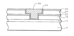
- a dual damascene opening is etched through the first and second dielectric layers, the capping layer and the etch stop layer, using one of the various schemes such as trench-first, via-first, or embedded via.
- the dual damascene opening is then filled with a barrier metal layer 34 and a copper layer 36 by any of the conventional means, including physical or chemical vapor deposition and etchback or polishing or electroless plating, and so on.
- the pre-treatment process of the present invention can be used in the presence of an etch stop layer, in the presence of a capping layer, or in the presence of both an etch stop layer and a capping layer.
- the pre-treatment of the present invention can be used if a capping layer is present.
- FIG. 10 there is illustrated a portion of a partially completed integrated circuit device.
- a substrate 10 preferably composed of monocrystalline silicon.
- Device structures such as gate electrodes, source and drain regions, and metal interconnects, not shown, are formed in and on the substrate and covered with an insulating layer.
- a passivation or barrier layer 12 may be formed over the device structures to a thickness of between about 50 and 5000 Angstroms.
- the passivation layer may comprise silicon nitride, silicon carbide, silicon oxynitride, silicon dioxide, boron nitride, or BLOK (from Applied Materials), for example.
- a first low dielectric constant (k) material layer 18 is deposited over the passivation layer 12 to a thickness of between about 5000 and 50,000 Angstroms.
- the first low dielectric constant material may be a porous or non-porous carbon-doped silicon oxide (such as alkyl silsesquioxanes), a porous or non-porous doped silicon oxide film (such as fluorosilicate glass (FSG) or phosphosilicate glass (PSG)), porous or non-porous organic polymers, or porous or non-porous inorganic polymers.
- a porous or non-porous carbon-doped silicon oxide such as alkyl silsesquioxanes
- a porous or non-porous doped silicon oxide film such as fluorosilicate glass (FSG) or phosphosilicate glass (PSG)
- FSG fluorosilicate glass
- PSG phosphosilicate glass
- an etch stop layer or cap layer is to be deposited over the low-k material layer 18 .
- an etch stop layer or cap layer is to be deposited over the low-k material layer 18 .
- an etch stop layer or cap layer is to be deposited over the low-k material layer 18 .
- the etch stop or capping layer comprises a silicon-based dielectric film that is not silicon oxide. That is, silicon nitride, silicon carbide, silicon oxynitride, silsesquioxanes, or other silicon-based material that is not silicon oxide can be used. If silicon oxynitride is used, silicon-rich silicon oxynitride is preferred.
- the silicon-based film 23 illustrated in FIG. 11, can be deposited by chemical vapor deposition or spin-coating followed by baking and/or curing. The etch stop or capping layer 23 is deposited to a thickness of between about 50 and 5000 Angstroms.
- a second low-k material layer 24 is deposited over the etch stop layer 23 , as shown in FIG. 12 .
- a capping layer 26 is deposited over the low-k material layer 24 to a thickness of between about 50 and 5000 Angstroms.
- silicon nitride, silicon carbide, silsesquioxanes, silicon oxynitride, or other silicon-based material that is not silicon oxide can be used as the capping layer. If silicon oxynitride is used, silicon-rich silicon oxynitride is preferred.
- a dual damascene opening is etched through the first and second dielectric layers, the capping layer and the etch stop layer, using one of the various schemes such as trench-first, via-first, or embedded via.
- the dual damascene opening is then filled with a barrier metal layer 34 and a copper layer 36 by any of the conventional means, including physical or chemical vapor deposition and etchback or polishing or electroless plating, and so on.
- the process of the present invention using a silicon-based dielectric film, with the exception of silicon oxide, over the low-k material film provides improved adhesion of the etch stop and/or capping layer.
- the process of the present invention using pre-treatment of a low-k dielectric material film before depositing a TEOS layer thereover or using a silicon-based dielectric film, with the exception of silicon oxide, over the low-k material film provides dramatic adhesion improvement over the prior art.
- the adhesion improvement has been shown with a peel test and with a modified tape test (described in co-pending U.S. patent application Ser. No. 09/771,512 filed on Jan. 25, 2001).
Landscapes
- Engineering & Computer Science (AREA)
- Physics & Mathematics (AREA)
- Condensed Matter Physics & Semiconductors (AREA)
- General Physics & Mathematics (AREA)
- Manufacturing & Machinery (AREA)
- Computer Hardware Design (AREA)
- Microelectronics & Electronic Packaging (AREA)
- Power Engineering (AREA)
- Plasma & Fusion (AREA)
- Internal Circuitry In Semiconductor Integrated Circuit Devices (AREA)
- Local Oxidation Of Silicon (AREA)
Abstract
Method of improving adhesion of low dielectric constant films to other dielectric films and barrier metals in a damascene process are achieved. In one method, a low dielectric constant material layer is deposited on a substrate. Silicon ions are implanted into the low dielectric constant material layer. Thereafter, a TEOS-based silicon oxide layer is deposited overlying the low dielectric constant material whereby there is good adhesion between low dielectric constant material layer and the TEOS-based silicon oxide layer. In another method, a low dielectric constant material layer is deposited on a substrate. A silicon-based dielectric layer is deposited overlying the low dielectric constant material wherein the silicon-based dielectric layer is not silicon oxide whereby there is good adhesion between the low dielectric constant material layer and the silicon-based dielectric layer.
Description
(1) Field of the Invention
The invention relates to a method of metallization in the fabrication of integrated circuits, and more particularly, to a method of improving adhesion of low dielectric constant materials to other materials during metallization in the manufacture of integrated circuits.
(2) Description of the Prior Art
The damascene or dual damascene process has become a future trend in integrated circuit manufacturing, especially in the copper metallization process. In a typical copper damascene scheme, dielectric layers are formed over a passivation layer on a substrate. An etch stop layer may be formed between two dielectric layers and a cap layer may be formed over the topmost dielectric layer. A via and trench are patterned into the dielectric layers to the passivation layer. Then a barrier metal layer is deposited within the trench and via, followed by deposition of a copper layer to fill the damascene opening.
Low dielectric constant materials are preferably used to reduce capacitance. An integration challenge facing damascene interconnects incorporating low dielectric constant materials and copper is the adhesion of these low dielectric constant materials to other damascene films. Poor adhesion is a cause for reliability concerns. In recent experiments, the inventors have determined that tetraethoxysilane (TEOS)-based silicon oxide did not adhere well on carbon-doped silicon oxide materials such as alkyl silsesquioxanes and perhydrosilazanes. It is desired to find a method to improve adhesion of low dielectric constant materials with other dielectric materials.
U.S. Pat. No. 6,184,123 to Ge et al discloses a silicon ion implantation into spin-on-glass to improve adhesion to an overlying silicon nitride layer. U.S. Pat. No. 6,143,670 to Cheng et al shows a nitrogen ion implantation into a polymer layer to improve adhesion to an overlying layer containing silicon, oxygen, and nitrogen. U.S. Pat. No. 5,985,750 to Oda implants silicon ions into a BPSG layer to form a damage layer before depositing a fluorine amorphous carbon layer. U.S. Pat. No. 6,117,798 to Fang et al and U.S. Pat. No. 5,459,086 to Yang teach an ion implantation into spin-on-glass to prevent moisture absorption. U.S. Pat. No. 5,192,697 to Leong teaches curing of spin-on-glass using ion implantation. U.S. Pat. No. 4,849,248 to Hashimoto discloses silicon ion implantation into silicon dioxide to control grain size. U.S. Pat. No. 6,153,523 to Van Ngo et al shows the use of an ammonia-containing plasma to roughen a copper surface to improve adhesion of an overlying silicon nitride capping layer.
A principal object of the present invention is to provide an effective and very manufacturable method of improving adhesion of dielectric films in the fabrication of integrated circuit devices.
Another object of the invention is to provide a method of improving adhesion of dielectric films in a damascene metallization process.
Yet another object of the invention is to a method of improving adhesion of low dielectric constant films to other dielectric films in a damascene process.
In accordance with the objects of this invention a method of improving adhesion of low dielectric constant films to other dielectric films in a damascene process is achieved. A low dielectric constant material layer is deposited on a substrate. Silicon ions are implanted into the low dielectric constant material layer. Thereafter, a TEOS-based silicon oxide layer is deposited overlying the low dielectric constant material whereby there is good adhesion between low dielectric constant material layer and the TEOS-based silicon oxide layer.
Also, in accordance with the objects of the invention, another method of improving adhesion of low dielectric constant films to other dielectric films in a damascene process is achieved. A low dielectric constant material layer is deposited on a substrate. A silicon-based dielectric layer is deposited overlying the low dielectric constant material wherein the silicon-based dielectric layer is not silicon oxide whereby there is good adhesion between the low dielectric constant material layer and the silicon-based dielectric layer.
In the accompanying drawings forming a material part of this description, there is shown:
FIGS. 1 through 9 schematically illustrate in cross-sectional representation a first preferred embodiment of the present invention.
FIGS. 10 through 13 schematically illustrate in cross-sectional representation a second preferred embodiment of the present invention.
The present invention proposes two alternative methods of improving adhesion of low dielectric constant films to other dielectric films and barrier metals in a damascene process. It will be understood by those skilled in the art that the present invention should not be limited to the dual damascene application illustrated in the drawings, but can be extended and applied to any application in which improved adhesion of dielectric films is desired.
The first embodiment of the present invention comprises a pre-treatment of a low dielectric constant film before depositing a silicon oxide film. The first embodiment will be described with reference to FIGS. 1 through 9. The second embodiment of the invention comprises using a silicon-based dielectric film other than silicon oxide over a low dielectric constant film. The second embodiment will be described with reference to FIGS. 10 through 13.
The first embodiment of the present invention now will be described with reference to FIGS. 1 through 9. Referring now more particularly to FIG. 1, there is illustrated a portion of a partially completed integrated circuit device. There is shown a substrate 10, preferably composed of monocrystalline silicon. Device structures, such as gate electrodes, source and drain regions, and metal interconnects, not shown, are formed in and on the substrate and covered with an insulating layer. A passivation or barrier layer 12 may be formed over the device structures to a thickness of between about 50 and 5000 Angstroms. The passivation layer may comprise silicon nitride, silicon carbide, silicon oxynitride, silicon dioxide, boron nitride, or BLOK (from Applied Materials), for example.
Referring to FIG. 2, a first low dielectric constant (k) material layer 18 is deposited over the passivation layer 12 to a thickness of between about 500 and 50,000 Angstroms. The first low dielectric constant material may be a porous or non-porous carbon-doped silicon oxide (such as alkyl silsesquioxanes), a porous or non-porous doped silicon oxide film (such as fluorosilicate glass (FSG) and phosphosilicate glass (PSG)), porous or non-porous organic polymers, or porous or non-porous inorganic polymers.
Now, an etch stop layer or cap layer is to be deposited over the low-k material layer 18. For example, in a dual-damascene process, there is often an etch stop layer interposed between two low-k material layers. In a single damascene process, or in some cases in a dual damascene process, there may be no etch stop layer, but a capping layer over the topmost low-k material layer. Preferably in this embodiment, the etch stop or capping layer will be a TEOS-based silicon oxide layer. It has been found that for a TEOS-based silicon oxide layer having a thickness greater than 2000 Angstroms, poor adhesion to the underlying low-k material layer is experienced.
The inventors have experimented with various pre-treatments of the low-k material layer before deposition of the etch stop or capping layer. These pre-treatments included nitrogen plasma, argon implantation, silicon implantation, and phosphorus implantation. Only the silicon implantation resulted in non-peeling of the overlying TEOS-based oxide from the low-k material layer. A dramatic improvement in adhesion strength was observed. Further, the shallow implantation of the invention does not change the dielectric constant of the dielectric film, thus maintaining its integrity.
FIG. 2 illustrates the silicon implantation pre-treatment of the present invention. Silicon ions are implanted 20 into the low-k material layer at an energy of between about 5 and 30 Key with a dosage of between about 1 E 12 and 1 E 16 ions/cm2. The targeted mean depth of implantation is between about 50 and 600 Angetroms. FIG. 3 illustrates the roughened silicon-implanted surface 21 of the low-k material layer 18.
Referring now to FIG. 4, after pre-treatment of the low-k material layer 18, the etch stop or capping layer 22 is deposited to a thickness of between about 50 and 5000 Angstroms. The etch stop or capping layer 22 comprises TEOS-based silicon oxide.
If layer 22 is an etch stop layer, a second low-k material layer 24 is deposited over the etch stop layer 22, as shown in FIG. 5. Silicon ion implantation 25 is again performed as a pre-treatment of the second low-k material layer 24, as shown in FIG. 6.
The roughened surface 27 of the low-k material layer 24 is shown in FIG. 7. Now, a capping layer 30 is deposited over the treated low-k material layer 24 to a thickness of between about 50 and 5000 Angstroms, as illustrated in FIG. 8. The second ion implantation is necessary only if the optional capping layer 30 is to be deposited.
Now, as shown in FIG. 9, a dual damascene opening is etched through the first and second dielectric layers, the capping layer and the etch stop layer, using one of the various schemes such as trench-first, via-first, or embedded via. The dual damascene opening is then filled with a barrier metal layer 34 and a copper layer 36 by any of the conventional means, including physical or chemical vapor deposition and etchback or polishing or electroless plating, and so on.
The pre-treatment process of the present invention can be used in the presence of an etch stop layer, in the presence of a capping layer, or in the presence of both an etch stop layer and a capping layer. For example, in a single damascene process with no etch stop layer, the pre-treatment of the present invention can be used if a capping layer is present.
The second embodiment of the present invention will be described with reference to FIGS. 10 through 13. Referring now more particularly to FIG. 10, there is illustrated a portion of a partially completed integrated circuit device. There is shown a substrate 10, preferably composed of monocrystalline silicon. Device structures, such as gate electrodes, source and drain regions, and metal interconnects, not shown, are formed in and on the substrate and covered with an insulating layer.
A passivation or barrier layer 12 may be formed over the device structures to a thickness of between about 50 and 5000 Angstroms. The passivation layer may comprise silicon nitride, silicon carbide, silicon oxynitride, silicon dioxide, boron nitride, or BLOK (from Applied Materials), for example. A first low dielectric constant (k) material layer 18 is deposited over the passivation layer 12 to a thickness of between about 5000 and 50,000 Angstroms. The first low dielectric constant material may be a porous or non-porous carbon-doped silicon oxide (such as alkyl silsesquioxanes), a porous or non-porous doped silicon oxide film (such as fluorosilicate glass (FSG) or phosphosilicate glass (PSG)), porous or non-porous organic polymers, or porous or non-porous inorganic polymers.
Now, an etch stop layer or cap layer is to be deposited over the low-k material layer 18. For example, in a dual-damascene process, there is often an etch stop layer interposed between two low-k material layers. In a single damascene process, or in some cases in a dual damascene process, there may be no etch stop layer, but a capping layer over the topmost low-k material layer.
It has been found by the inventors that an improvement in adhesion can be obtained without the pre-treatment of the first embodiment if the etch stop or capping layer comprises a silicon-based dielectric film that is not silicon oxide. That is, silicon nitride, silicon carbide, silicon oxynitride, silsesquioxanes, or other silicon-based material that is not silicon oxide can be used. If silicon oxynitride is used, silicon-rich silicon oxynitride is preferred. The silicon-based film 23, illustrated in FIG. 11, can be deposited by chemical vapor deposition or spin-coating followed by baking and/or curing. The etch stop or capping layer 23 is deposited to a thickness of between about 50 and 5000 Angstroms.
If layer 23 is an etch stop layer, a second low-k material layer 24 is deposited over the etch stop layer 23, as shown in FIG. 12. Now, a capping layer 26 is deposited over the low-k material layer 24 to a thickness of between about 50 and 5000 Angstroms. Again, silicon nitride, silicon carbide, silsesquioxanes, silicon oxynitride, or other silicon-based material that is not silicon oxide can be used as the capping layer. If silicon oxynitride is used, silicon-rich silicon oxynitride is preferred.
Now, as shown in FIG. 13, a dual damascene opening is etched through the first and second dielectric layers, the capping layer and the etch stop layer, using one of the various schemes such as trench-first, via-first, or embedded via. The dual damascene opening is then filled with a barrier metal layer 34 and a copper layer 36 by any of the conventional means, including physical or chemical vapor deposition and etchback or polishing or electroless plating, and so on.
The process of the present invention, using a silicon-based dielectric film, with the exception of silicon oxide, over the low-k material film provides improved adhesion of the etch stop and/or capping layer.
The process of the present invention, using pre-treatment of a low-k dielectric material film before depositing a TEOS layer thereover or using a silicon-based dielectric film, with the exception of silicon oxide, over the low-k material film provides dramatic adhesion improvement over the prior art. The adhesion improvement has been shown with a peel test and with a modified tape test (described in co-pending U.S. patent application Ser. No. 09/771,512 filed on Jan. 25, 2001).
While the invention has been particularly shown and described with reference to the preferred embodiments thereof, it will be understood by those skilled in the art that various changes in form and details may be made without departing from the spirit and scope of the invention.
Claims (19)
1. A method of forming a dielectric material layer comprising:
depositing a low dielectric constant material layer on a passivation layer on a substrate wherein said low dielectric constant material is selected from the group consisting of: porous or non-porous carbon-based silicon oxides, porous or non-porous organic polymers, and porous or non-porous inorganic polymers;
implanting silicon ions into said low dielectric constant material; and
thereafter depositing a TEOS-based silicon oxide layer overlying said low dielectric constant material whereby there is good adhesion between said low dielectric constant material layer and said TEOS-based silicon oxide layer.
2. The method according to claim 1 wherein said low dielectric constant material layer has a thickness of between about 500 and 50,000 Angstroms.
3. The method according to claim 1 wherein said step of implanting silicon ions into said low dielectric constant material layer comprises implanting said silicon ions at an energy of between about 5 and 30 KeV at a dosage of between about 1 E 12 and 1 E 16 ions/cm2.
4. The method according to claim 1 wherein said TEOS-based silicon oxide layer has a thickness of between about 50 and 5000 Angstroms.
5. A method of dual damascene copper metallization in the fabrication of an integrated circuit device comprising:
depositing a first low dielectric constant material layer over a substrate wherein said first low dielectric constant material is selected from the group consisting of: alkyl silsesquioxanes, porous or non-porous organic polymers, and porous or non-porous inorganic polymers;
implanting silicon ions into said first low dielectric constant material layer;
thereafter depositing a TEOS-based silicon oxide etch stop layer overlying said first low dielectric constant material whereby there is good adhesion between said first low dielectric constant material layer and said TEOS-based silicon oxide etch stop layer;
depositing a second low dielectric constant material layer overlying said etch stop layer wherein said second low dielectric constant material is selected from the group consisting of: alkyl silsesquioxanes, porous or non-porous organic polymers, and porous or non-porous inorganic polymers;
implanting silicon ions into said second low dielectric constant material layer;
thereafter depositing a TEOS-based silicon oxide capping layer overlying said second low dielectric constant material whereby there is good adhesion between said second low dielectric constant material layer and said TEOS-based silicon oxide capping layer;
forming a dual damascene opening through said capping layer, said second low dielectric constant material layer, said etch stop layer, and said first low dielectric constant material layer; and
forming a barrier metal layer and a copper layer within said dual damascene opening to complete said copper metallization in the fabrication of said integrated circuit device.
6. The method according to claim 5 wherein said first and second low dielectric constant material layers have a thickness of between about 500 and 50,000 Angstroms.
7. The method according to claim 5 wherein said steps of implanting silicon ions into said first and second low dielectric constant material layers comprises implanting said silicon ions at an energy of between about 5 and 30 KeV at a dosage of between about 1 E 12 and 1 E 16 ions/cm2.
8. The method according to claim 5 wherein said silicon ions are implanted into said first and second low dielectric constant material layers to a depth of between about 50 and 600 Angstroms thereby forming a roughened silicon-implanted surface of said first and second low dielectric constant material layers.
9. The method according to claim 5 wherein said TEOS-based silicon oxide etch stop layer has a thickness of between about 50 and 5000 Angstroms.
10. The method according to claim 5 wherein said TEOS-based silicon oxide capping layer has a thickness of between about 50 and 5000 Angstroms.
11. A method of forming a dielectric material layer comprising:
depositing a low dielectric constant material layer on a substrate wherein said low dielectric constant material is selected from the group consisting of: alkyl silsesquioxanes, porous or non-porous organic polymers, and porous or non-porous inorganic polymers;
implanting silicon ions into said low dielectric constant material layer to a depth of between about 50 and 600 Angstroms thereby forming a roughened silicon-implanted surface of said low dielectric constant material layer; and
thereafter depositing a TEOS-based silicon oxide layer ovrerlying said roughened surface of said low dielectric constant material whereby there is good adhesion between said low dielectric constant material layer and said TBOS-based silicon oxide layer.
12. The method according to claim 11 wherein said low dielectric constant material layer has a thickness of between about 500 and 50,000 Angstroms.
13. The method according to claim 11 wherein said step of implanting silicon ions into said low dielectric constant material layer comprises implanting said silicon ions at an energy of between about 5 and 30 KeV at a dosage of between about 1 E 12 and 1 E 16 ions/cm2.
14. The method according to claim 11 wherein said TEOS-based silicon oxide layer has a thickness of betWeen about 50 and 5000 Angstroms.
15. A method of dual damascene copper metallization in the fabrication of an integrated circuit device comprising:
depositing a first low dielectric constant material layer over a substrate wherein said first low dielectric constant material is selected from the group consisting of: alkyl silsesquioxanes, porous or non-porous organic polymers, and porous or non-porous inorganic polymers;
implanting silicon ions into said first low dielectric constant material layer to a depth of between about 50 and 600 Angstroms;
thereafter depositing a TEOS-based silicon oxide etch stop layer overlying said first low dielectric constant material whereby there is good adhesion between said first low dielectric constant material layer and said TEOS-based silicon oxide etch stop layer;
depositing a second low dielectric constant material layer overlying said etch stop layer wherein said second low dielectric constant material is selected from: alkyl silsesquioxanes, porous or non-porous organic polymers, and porous or non-porous inorganic polymers;
implanting silicon ions into said second low dielectric constant material layer to a depth of between about 50 and 600 Angstroms;
thereafter depositing a TEOS-based silicon oxide capping layer overlying said second low dielectric constant material whereby there is good adhesion between said second low dielectric constant material layer and said TEOS-based silicon oxide capping layer;
forming a dual damascene opening through said capping layer, said second low dielectric constant material layer, said etch stop layer, and said first low dielectric constant material layer; and
forming a barrier metal layer and a copper layer within said, dual damascene opening to complete said copper metallization in the fabrication of said integrated circuit device.
16. The method according to claim 15 wherein said first and second low dielectric constant material layers have a thickness of between about 500 and 50,000 Angstroms.
17. The method according to claim 15 wherein said steps of implanting silicon ions into said first and second low dielectric constant material layers comprises implanting said silicon ions at an energy of between about 5 and 30 KeV at a dosage of between about 1 E 12 and 1 E 16 ions/cm2.
18. The method according to claim 15 wherein said TEOS-based silicon oxide etch stop layer has a thickness of between about 50 and 5000 Angstroms.
19. The method according to claim 15 wherein said TEOS-based silicon oxide capping layer has a thickness of between about 50 and 5000 Angstroms.
Priority Applications (4)
| Application Number | Priority Date | Filing Date | Title |
|---|---|---|---|
| US09/912,737 US6797605B2 (en) | 2001-07-26 | 2001-07-26 | Method to improve adhesion of dielectric films in damascene interconnects |
| SG200203416A SG121716A1 (en) | 2001-07-26 | 2002-06-10 | A method to improve adhesion of dielectric films in damascene interconnects |
| SG200502891-5A SG136807A1 (en) | 2001-07-26 | 2002-06-10 | A method to improve adhesion of dielectric films in damascene interconnects |
| US10/943,101 US7078333B2 (en) | 2001-07-26 | 2004-09-16 | Method to improve adhesion of dielectric films in damascene interconnects |
Applications Claiming Priority (1)
| Application Number | Priority Date | Filing Date | Title |
|---|---|---|---|
| US09/912,737 US6797605B2 (en) | 2001-07-26 | 2001-07-26 | Method to improve adhesion of dielectric films in damascene interconnects |
Related Child Applications (1)
| Application Number | Title | Priority Date | Filing Date |
|---|---|---|---|
| US10/943,101 Division US7078333B2 (en) | 2001-07-26 | 2004-09-16 | Method to improve adhesion of dielectric films in damascene interconnects |
Publications (2)
| Publication Number | Publication Date |
|---|---|
| US20030022472A1 US20030022472A1 (en) | 2003-01-30 |
| US6797605B2 true US6797605B2 (en) | 2004-09-28 |
Family
ID=25432360
Family Applications (2)
| Application Number | Title | Priority Date | Filing Date |
|---|---|---|---|
| US09/912,737 Expired - Lifetime US6797605B2 (en) | 2001-07-26 | 2001-07-26 | Method to improve adhesion of dielectric films in damascene interconnects |
| US10/943,101 Expired - Fee Related US7078333B2 (en) | 2001-07-26 | 2004-09-16 | Method to improve adhesion of dielectric films in damascene interconnects |
Family Applications After (1)
| Application Number | Title | Priority Date | Filing Date |
|---|---|---|---|
| US10/943,101 Expired - Fee Related US7078333B2 (en) | 2001-07-26 | 2004-09-16 | Method to improve adhesion of dielectric films in damascene interconnects |
Country Status (2)
| Country | Link |
|---|---|
| US (2) | US6797605B2 (en) |
| SG (2) | SG121716A1 (en) |
Cited By (9)
| Publication number | Priority date | Publication date | Assignee | Title |
|---|---|---|---|---|
| US20030227087A1 (en) * | 2002-06-07 | 2003-12-11 | Fujitsu Limited | Semiconductor device and method of manufacturing the same |
| US20040266184A1 (en) * | 2003-06-30 | 2004-12-30 | Ramachandrarao Vijayakumar S | Post-deposition modification of interlayer dielectrics |
| US20050040532A1 (en) * | 2003-08-21 | 2005-02-24 | International Business Machines Corporation | Dual damascene integration of ultra low dielectric constant porous materials |
| US20050272260A1 (en) * | 2004-06-04 | 2005-12-08 | Taiwan Semiconductor Manufacturing Co. | Novel device structure having enhanced surface adhesion and failure mode analysis |
| US20070249159A1 (en) * | 2006-04-24 | 2007-10-25 | Taiwan Semiconductor Manufacturing Company, Ltd. | Method for forming dielectric film to improve adhesion of low-k film |
| US20080299718A1 (en) * | 2007-06-01 | 2008-12-04 | Texas Instruments Incorporated | Damascene process having retained capping layer through metallization for protecting low-k dielectrics |
| US8927869B2 (en) | 2012-04-11 | 2015-01-06 | International Business Machines Corporation | Semiconductor structures and methods of manufacture |
| USRE45781E1 (en) * | 2001-12-13 | 2015-10-27 | GlobalFoundries, Inc. | Toughness, adhesion and smooth metal lines of porous low K dielectric interconnect structures |
| US11640950B2 (en) | 2020-09-09 | 2023-05-02 | Samsung Electronics Co., Ltd. | Semiconductor chip and semiconductor package |
Families Citing this family (6)
| Publication number | Priority date | Publication date | Assignee | Title |
|---|---|---|---|---|
| US7071129B2 (en) * | 2002-09-12 | 2006-07-04 | Intel Corporation | Enhancing adhesion of silicon nitride films to carbon-containing oxide films |
| DE102006046381B4 (en) * | 2006-09-29 | 2009-08-27 | Advanced Micro Devices, Inc., Sunnyvale | A method of reducing "paint poisoning" during patterning strained nitrogen-containing layers in a semiconductor device |
| DE102007041220B3 (en) * | 2007-08-31 | 2009-01-08 | Advanced Micro Devices, Inc., Sunnyvale | Method for manufacturing semiconductor components with field-effect transistors, involves forming stress inducing dielectric layer over multiple p-channel transistors |
| US8790751B2 (en) * | 2008-04-16 | 2014-07-29 | Spansion Llc | Method of improving adhesion of dielectric cap to copper |
| US11508857B2 (en) * | 2019-02-04 | 2022-11-22 | University Of Florida Research Foundation, Incorporated | Optical scrambler with nano-pyramids |
| US11201134B2 (en) * | 2020-04-20 | 2021-12-14 | United Microelectronics Corp. | Method of manufacturing semiconductor device |
Citations (17)
| Publication number | Priority date | Publication date | Assignee | Title |
|---|---|---|---|---|
| US4849248A (en) | 1985-12-02 | 1989-07-18 | Texas Instruments Incorporated | Ion implantation method for making silicon-rich silicon dioxide film |
| US5192697A (en) | 1992-01-27 | 1993-03-09 | Chartered Semiconductor Manufacturing Pte Ltd. | SOG curing by ion implantation |
| JPH05129280A (en) * | 1991-10-31 | 1993-05-25 | Sony Corp | Manufacture of semiconductor device |
| US5459086A (en) | 1994-11-07 | 1995-10-17 | United Microelectronics Corporation | Metal via sidewall tilt angle implant for SOG |
| JPH08102489A (en) * | 1994-09-30 | 1996-04-16 | Ricoh Co Ltd | Manufacture of semiconductor device and semiconductor device |
| US5554567A (en) * | 1994-09-01 | 1996-09-10 | Taiwan Semiconductor Manufacturing Company Ltd. | Method for improving adhesion to a spin-on-glass |
| US5985750A (en) | 1997-05-23 | 1999-11-16 | Nec Corporation | Manufacturing method of semiconductor device |
| US6117798A (en) | 1998-12-16 | 2000-09-12 | United Microelectronics Corp. | Method of spin-on-glass planarization |
| US6143670A (en) | 1998-12-28 | 2000-11-07 | Taiwan Semiconductor Manufacturing Company | Method to improve adhesion between low dielectric constant layer and silicon containing dielectric layer |
| US6153523A (en) | 1998-12-09 | 2000-11-28 | Advanced Micro Devices, Inc. | Method of forming high density capping layers for copper interconnects with improved adhesion |
| US6153512A (en) * | 1999-10-12 | 2000-11-28 | Taiwan Semiconductor Manufacturing Company | Process to improve adhesion of HSQ to underlying materials |
| US6184123B1 (en) | 1999-08-02 | 2001-02-06 | Taiwan Semiconductor Manufacturing Company | Method to prevent delamination of spin-on-glass and plasma nitride layers using ion implantation |
| US6214749B1 (en) * | 1994-09-14 | 2001-04-10 | Sanyo Electric Co., Ltd. | Process for producing semiconductor devices |
| US6316348B1 (en) * | 1999-02-05 | 2001-11-13 | Taiwan Semiconductor Manufacturing Company | High selectivity Si-rich SiON etch-stop layer |
| US6558747B2 (en) * | 1999-09-29 | 2003-05-06 | Kabushiki Kaisha Toshiba | Method of forming insulating film and process for producing semiconductor device |
| US6583071B1 (en) * | 1999-10-18 | 2003-06-24 | Applied Materials Inc. | Ultrasonic spray coating of liquid precursor for low K dielectric coatings |
| US6589610B2 (en) * | 1996-05-13 | 2003-07-08 | Applied Materials, Inc. | Deposition chamber and method for depositing low dielectric constant films |
Family Cites Families (3)
| Publication number | Priority date | Publication date | Assignee | Title |
|---|---|---|---|---|
| KR100265771B1 (en) * | 1998-07-09 | 2000-10-02 | 윤종용 | Method for metallization by dual damascene process using photosensitive polymer |
| FR2802336B1 (en) * | 1999-12-13 | 2002-03-01 | St Microelectronics Sa | DAMASCENE-TYPE INTERCONNECTION STRUCTURE AND ITS MANUFACTURING METHOD |
| US6358842B1 (en) * | 2000-08-07 | 2002-03-19 | Chartered Semiconductor Manufacturing Ltd. | Method to form damascene interconnects with sidewall passivation to protect organic dielectrics |
-
2001
- 2001-07-26 US US09/912,737 patent/US6797605B2/en not_active Expired - Lifetime
-
2002
- 2002-06-10 SG SG200203416A patent/SG121716A1/en unknown
- 2002-06-10 SG SG200502891-5A patent/SG136807A1/en unknown
-
2004
- 2004-09-16 US US10/943,101 patent/US7078333B2/en not_active Expired - Fee Related
Patent Citations (17)
| Publication number | Priority date | Publication date | Assignee | Title |
|---|---|---|---|---|
| US4849248A (en) | 1985-12-02 | 1989-07-18 | Texas Instruments Incorporated | Ion implantation method for making silicon-rich silicon dioxide film |
| JPH05129280A (en) * | 1991-10-31 | 1993-05-25 | Sony Corp | Manufacture of semiconductor device |
| US5192697A (en) | 1992-01-27 | 1993-03-09 | Chartered Semiconductor Manufacturing Pte Ltd. | SOG curing by ion implantation |
| US5554567A (en) * | 1994-09-01 | 1996-09-10 | Taiwan Semiconductor Manufacturing Company Ltd. | Method for improving adhesion to a spin-on-glass |
| US6214749B1 (en) * | 1994-09-14 | 2001-04-10 | Sanyo Electric Co., Ltd. | Process for producing semiconductor devices |
| JPH08102489A (en) * | 1994-09-30 | 1996-04-16 | Ricoh Co Ltd | Manufacture of semiconductor device and semiconductor device |
| US5459086A (en) | 1994-11-07 | 1995-10-17 | United Microelectronics Corporation | Metal via sidewall tilt angle implant for SOG |
| US6589610B2 (en) * | 1996-05-13 | 2003-07-08 | Applied Materials, Inc. | Deposition chamber and method for depositing low dielectric constant films |
| US5985750A (en) | 1997-05-23 | 1999-11-16 | Nec Corporation | Manufacturing method of semiconductor device |
| US6153523A (en) | 1998-12-09 | 2000-11-28 | Advanced Micro Devices, Inc. | Method of forming high density capping layers for copper interconnects with improved adhesion |
| US6117798A (en) | 1998-12-16 | 2000-09-12 | United Microelectronics Corp. | Method of spin-on-glass planarization |
| US6143670A (en) | 1998-12-28 | 2000-11-07 | Taiwan Semiconductor Manufacturing Company | Method to improve adhesion between low dielectric constant layer and silicon containing dielectric layer |
| US6316348B1 (en) * | 1999-02-05 | 2001-11-13 | Taiwan Semiconductor Manufacturing Company | High selectivity Si-rich SiON etch-stop layer |
| US6184123B1 (en) | 1999-08-02 | 2001-02-06 | Taiwan Semiconductor Manufacturing Company | Method to prevent delamination of spin-on-glass and plasma nitride layers using ion implantation |
| US6558747B2 (en) * | 1999-09-29 | 2003-05-06 | Kabushiki Kaisha Toshiba | Method of forming insulating film and process for producing semiconductor device |
| US6153512A (en) * | 1999-10-12 | 2000-11-28 | Taiwan Semiconductor Manufacturing Company | Process to improve adhesion of HSQ to underlying materials |
| US6583071B1 (en) * | 1999-10-18 | 2003-06-24 | Applied Materials Inc. | Ultrasonic spray coating of liquid precursor for low K dielectric coatings |
Cited By (17)
| Publication number | Priority date | Publication date | Assignee | Title |
|---|---|---|---|---|
| USRE45781E1 (en) * | 2001-12-13 | 2015-10-27 | GlobalFoundries, Inc. | Toughness, adhesion and smooth metal lines of porous low K dielectric interconnect structures |
| US20030227087A1 (en) * | 2002-06-07 | 2003-12-11 | Fujitsu Limited | Semiconductor device and method of manufacturing the same |
| US20040266184A1 (en) * | 2003-06-30 | 2004-12-30 | Ramachandrarao Vijayakumar S | Post-deposition modification of interlayer dielectrics |
| US7338895B2 (en) | 2003-08-21 | 2008-03-04 | International Business Machines Corporation | Method for dual damascene integration of ultra low dielectric constant porous materials |
| US20050040532A1 (en) * | 2003-08-21 | 2005-02-24 | International Business Machines Corporation | Dual damascene integration of ultra low dielectric constant porous materials |
| US20060118961A1 (en) * | 2003-08-21 | 2006-06-08 | International Business Machines Corp. | Dual damascene integration of ultra low dielectric constant porous materials |
| US20080099923A1 (en) * | 2003-08-21 | 2008-05-01 | International Business Machines Corporation | Dual damascene integration of ultra low dielectric constant porous materials |
| US7057287B2 (en) * | 2003-08-21 | 2006-06-06 | International Business Machines Corporation | Dual damascene integration of ultra low dielectric constant porous materials |
| US7737561B2 (en) | 2003-08-21 | 2010-06-15 | International Business Machines Corporation | Dual damascene integration of ultra low dielectric constant porous materials |
| US7157367B2 (en) * | 2004-06-04 | 2007-01-02 | Taiwan Semiconductor Manufacturing Co., Ltd. | Device structure having enhanced surface adhesion and failure mode analysis |
| US20050272260A1 (en) * | 2004-06-04 | 2005-12-08 | Taiwan Semiconductor Manufacturing Co. | Novel device structure having enhanced surface adhesion and failure mode analysis |
| US20070249159A1 (en) * | 2006-04-24 | 2007-10-25 | Taiwan Semiconductor Manufacturing Company, Ltd. | Method for forming dielectric film to improve adhesion of low-k film |
| US7465676B2 (en) | 2006-04-24 | 2008-12-16 | Taiwan Semiconductor Manufacturing Company, Ltd. | Method for forming dielectric film to improve adhesion of low-k film |
| US20080299718A1 (en) * | 2007-06-01 | 2008-12-04 | Texas Instruments Incorporated | Damascene process having retained capping layer through metallization for protecting low-k dielectrics |
| US8927869B2 (en) | 2012-04-11 | 2015-01-06 | International Business Machines Corporation | Semiconductor structures and methods of manufacture |
| US9230929B2 (en) | 2012-04-11 | 2016-01-05 | Globalfoundries Inc. | Semiconductor structures and methods of manufacture |
| US11640950B2 (en) | 2020-09-09 | 2023-05-02 | Samsung Electronics Co., Ltd. | Semiconductor chip and semiconductor package |
Also Published As
| Publication number | Publication date |
|---|---|
| SG136807A1 (en) | 2007-11-29 |
| SG121716A1 (en) | 2006-05-26 |
| US20050032392A1 (en) | 2005-02-10 |
| US20030022472A1 (en) | 2003-01-30 |
| US7078333B2 (en) | 2006-07-18 |
Similar Documents
| Publication | Publication Date | Title |
|---|---|---|
| US6797605B2 (en) | Method to improve adhesion of dielectric films in damascene interconnects | |
| US5496776A (en) | Spin-on-glass planarization process with ion implantation | |
| US8445377B2 (en) | Mechanically robust metal/low-k interconnects | |
| US6531390B2 (en) | Non-metallic barrier formations for copper damascene type interconnects | |
| US8158521B2 (en) | Two step post-deposition treatment of ILD layer for a lower dielectric constant and improved mechanical properties | |
| US6143670A (en) | Method to improve adhesion between low dielectric constant layer and silicon containing dielectric layer | |
| US8183166B2 (en) | Dielectric layer structure and manufacturing method thereof | |
| US7480990B2 (en) | Method of making conductor contacts having enhanced reliability | |
| US6143666A (en) | Plasma surface treatment method for forming patterned TEOS based silicon oxide layer with reliable via and interconnection formed therethrough | |
| EP0881678A2 (en) | Improvements in or relating to porous dielectric structures | |
| US6503818B1 (en) | Delamination resistant multi-layer composite dielectric layer employing low dielectric constant dielectric material | |
| TWI424493B (en) | Integrated circuit system employing low-k dielectrics and method of manufacture thereof | |
| JPH1074755A (en) | Microelectronic structure and its forming method | |
| US6794693B2 (en) | Semiconductor device and manufacturing method thereof | |
| JP4058135B2 (en) | Contact hole forming method for semiconductor device | |
| US6998343B1 (en) | Method for creating barrier layers for copper diffusion | |
| TWI229918B (en) | Method of forming an inter-metal dielectric layer in an interconnect structure | |
| US6800928B1 (en) | Porous integrated circuit dielectric with decreased surface porosity | |
| EP1037271A2 (en) | Method for forming an interlayer insulating film, and semiconductor device | |
| US7144828B2 (en) | He treatment to improve low-k adhesion property | |
| US6917110B2 (en) | Semiconductor device comprising an interconnect structure with a modified low dielectric insulation layer | |
| US6211062B1 (en) | Method for manufacturing semiconductor device having multiple wiring layer | |
| US7442653B2 (en) | Inter-metal dielectric of semiconductor device and manufacturing method thereof including plasma treating a plasma enhanced fluorosilicate glass | |
| US7071129B2 (en) | Enhancing adhesion of silicon nitride films to carbon-containing oxide films | |
| CN1669137A (en) | Semiconductor device and method of manufacturing the same |
Legal Events
| Date | Code | Title | Description |
|---|---|---|---|
| AS | Assignment |
Owner name: CHARTERED SEMICONDUCTOR MANUFACTURING LTD., SINGAP Free format text: ASSIGNMENT OF ASSIGNORS INTEREST;ASSIGNORS:GOH, LUONA;CHOOI, SIMON;TOH, SIEW LOK;AND OTHERS;REEL/FRAME:012044/0988 Effective date: 20010720 |
|
| STCF | Information on status: patent grant |
Free format text: PATENTED CASE |
|
| FPAY | Fee payment |
Year of fee payment: 4 |
|
| FPAY | Fee payment |
Year of fee payment: 8 |
|
| FPAY | Fee payment |
Year of fee payment: 12 |