US6778141B1 - Patch antenna with increased bandwidth - Google Patents
Patch antenna with increased bandwidth Download PDFInfo
- Publication number
- US6778141B1 US6778141B1 US10/379,708 US37970803A US6778141B1 US 6778141 B1 US6778141 B1 US 6778141B1 US 37970803 A US37970803 A US 37970803A US 6778141 B1 US6778141 B1 US 6778141B1
- Authority
- US
- United States
- Prior art keywords
- patch
- line
- antenna
- patch antenna
- gap
- Prior art date
- Legal status (The legal status is an assumption and is not a legal conclusion. Google has not performed a legal analysis and makes no representation as to the accuracy of the status listed.)
- Expired - Fee Related
Links
Images


Classifications
-
- H—ELECTRICITY
- H01—ELECTRIC ELEMENTS
- H01Q—ANTENNAS, i.e. RADIO AERIALS
- H01Q9/00—Electrically-short antennas having dimensions not more than twice the operating wavelength and consisting of conductive active radiating elements
- H01Q9/04—Resonant antennas
- H01Q9/0407—Substantially flat resonant element parallel to ground plane, e.g. patch antenna
- H01Q9/045—Substantially flat resonant element parallel to ground plane, e.g. patch antenna with particular feeding means
-
- H—ELECTRICITY
- H01—ELECTRIC ELEMENTS
- H01Q—ANTENNAS, i.e. RADIO AERIALS
- H01Q5/00—Arrangements for simultaneous operation of antennas on two or more different wavebands, e.g. dual-band or multi-band arrangements
- H01Q5/30—Arrangements for providing operation on different wavebands
- H01Q5/307—Individual or coupled radiating elements, each element being fed in an unspecified way
- H01Q5/342—Individual or coupled radiating elements, each element being fed in an unspecified way for different propagation modes
- H01Q5/357—Individual or coupled radiating elements, each element being fed in an unspecified way for different propagation modes using a single feed point
- H01Q5/364—Creating multiple current paths
Definitions
- the present invention relates to patch antennas and more particularly to an improved patch antenna with increased bandwidth.
- an antenna is used in transmitting electromagnetic waves (i.e., signals) generated by an electronic device to the air or receiving signals by the electronic device.
- electromagnetic waves i.e., signals
- antennas have been widely provided in various electronic devices as ubiquitous elements.
- a quality of transmitted or received signal strongly depends on performance of an antenna provided in the electronic device or whether an antenna characteristic is matched with the electronic device.
- a high performance radio frequency (RF) circuit and digital circuit of an electronic device can be carried out only by incorporating a high quality antenna.
- RF radio frequency
- antennas are classified based on their structures and characteristics as detailed below.
- a patch antenna 10 comprises a substrate 11 made of ceramic material.
- the substrate 11 is formed by heating a ceramic material, molding the melted ceramic material to produce a ceramic plate, and finally sintering the ceramic plate.
- a patch 12 and a ground plane 13 both of rectangle or square are printed on top and bottom surfaces of the substrate 11 by photolithography and etching respectively.
- a feed pin 14 is pierced through the patch 12 and the ground plane 13 to connect to a signal wave feed line (e.g., coaxial cable) 15 .
- a signal wave feed line e.g., coaxial cable
- the electromagnetic field is then radiated from a gap between the patch 12 and the ground plane 13 .
- the patch antenna 10 is advantageous due to compactness, enhanced structural strength, high dielectric coefficient and low temperature coefficient of ceramic, good heat-resistant characteristic, low power loss, and applicable to various environments.
- a typical implementation of the patch antenna 10 is a ceramic patch antenna provided in a GSM (Global System for Mobile) based cellular phone.
- GSM Global System for Mobile
- the patch antenna 10 also has a number of disadvantages. For example, a manufacturing process of the patch antenna 10 is complicated, resulting in a high manufacturing cost.
- the signal wave feed line 15 such as coaxial cable has several drawbacks, e.g., time consuming in installation, the requisite provision of the additional feed pin 14 , a welding of the feed pin 14 to the patch 12 and the substrate 11 , and poor antenna quality caused by failed welding.
- a patch antenna 20 comprises a substrate 21 formed on a circuit board.
- a patch 22 and a ground plane 23 both of rectangle or square are printed on top and bottom surfaces of the substrate 21 by photolithography and etching respectively.
- a patch line 24 is extended from a center of a side of the patch 22 to an edge of the substrate 21 so as to serve as a signal wave feed line.
- a gap 221 is formed at either side of the patch line 24 to separate the patch line 24 from the patch 22 .
- a substantially W-shaped (i.e., circuitous) current path W indicated by dash line is formed along edges of the patch 22 and patch line 24 adjacent the gaps 221 .
- Such arrangement can increase the current path W, resulting in a size reduction of the patch antenna 20 .
- a very large inductance is generated by the circuitous current path W caused by forming the gaps 221 and the current path W passing two projections 222 each adjacent the gap 221 .
- the strong inductance will adversely affect gain and bandwidth of the patch antenna 20 , resulting in a prohibition of bandwidth increase.
- a patch antenna 30 comprises a substrate 31 formed on a circuit board.
- a patch 32 and a ground plane 33 both of rectangle or square are printed on top and bottom surfaces of the substrate 31 by photolithography and etching respectively.
- a space 331 is formed in the ground plane 33 .
- a patch line 34 is printed in the space 331 .
- a signal wave feed line is coupled to the patch 32 from one end of the patch line 34 by means of a coplanar wave-guide.
- such antenna is undesirable due to complicated structure, design difficulty, tedious manufacturing process, and high cost.
- a primary object of the present invention is to provide a patch antenna with increased bandwidth.
- One object of the present invention is to provide a patch antenna including a patch and a ground plane printed on top and bottom surfaces of a dielectric substrate respectively by a technique the same as manufacturing a printed circuit board.
- the patch has a size smaller than that of the dielectric substrate.
- the antenna further comprises a patch line extended from a center of a side of the patch to an edge of the dielectric substrate for serving as a signal wave feed line of the patch antenna, and a gap provided at one side of the patch line to separate the patch line from the patch for forming a circuitous current path from one edge of the patch line along the sides adjacent the gap to one side of the patch.
- the size and the shape of the gap between the one side of the patch line and the patch can be modified so as to obtain an improved signal matching.
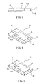
- FIG. 1 is a perspective view of a conventional patch antenna
- FIG. 2 is a perspective view of another conventional patch antenna having a patch line as feed line;
- FIG. 3 is a perspective view of a further conventional patch antenna having a coplanar wave-guide as feed line;
- FIG. 4 is a top plan view of a first preferred embodiment of patch antenna according to the invention.
- FIG. 5 is a cross-sectional view taken along line X—X of FIG. 4;
- FIG. 6 is a perspective view of a second preferred embodiment of patch antenna according to the invention.
- FIG. 7 is a perspective view of a third preferred embodiment of patch antenna according to the invention.
- FIG. 8 is a graph showing test result obtained by the patch antenna of FIG. 4;
- FIG. 9 is a graph showing test result obtained by the patch antenna of FIG. 6;
- FIG. 10 is a graph showing test result obtained by the patch antenna of FIG. 7.
- FIG. 11 is a graph showing test result obtained by the well-known patch antenna of FIG. 2 taken as comparison with that obtained by the embodiments of the invention.
- the patch antenna 40 comprises a patch 41 and a ground plane 42 printed on top and bottom surfaces of a dielectric substrate 43 respectively by a technique the same as manufacturing a printed circuit board.
- the patch 41 has a size smaller than the dielectric substrate 43 .
- a patch line 44 is extended from a center of a side of the patch 41 to an edge of the dielectric substrate 43 so as to serve as a signal wave feed line of the patch antenna 40 .
- a gap 411 is formed by etching at one side of the patch line 44 to separate the patch line 44 from the patch 41 .
- a circuitous current path W indicated by dash line is formed along one edge of the patch line 44 adjacent the side of the gap 411 to one side of the patch adjacent thereto.
- An inductance is generated by the circuitous current path W from one edge of the patch line 44 to a patch section 412 along the sides adjacent the gap 411 . Further, no strong inductance is generated by current passing from another edge of the patch line 44 to another patch section 413 . As a result, both gain and bandwidth of the patch antenna 40 are increased significantly.
- the manufacturing process of the first preferred embodiment of the invention comprises forming the patch 41 , the ground plane 42 , the patch line 44 , and the gap 411 on a circuit board.
- the manufacturing process is simple and easy.
- the produced patch antenna 40 has a larger effective bandwidth.
- it is permitted to adjust the shape and the size of the gap 411 depending on applications in manufacturing the patch antenna 40 according to the invention.
- the current path W passing the patch section 412 and the gap 411 and the generated inductance can be controlled.
- both the gain and the bandwidth of the patch antenna 40 can be increased for complying with the product specifications.
- the gap 411 at one side of the patch line 44 can be formed as an enlarged one toward its opening depending on requirements of the gain and the bandwidth of the patch antenna 40 .
- a circuitous current path W from one edge of the patch line 44 to the patch section 412 along the sides adjacent the gap 411 can be further away from the current path passed the patch line 44 .
- This can significantly decrease an undesired inductance effect on the signal.
- the gain of the patch antenna 40 is increased significantly and a good signal matching is obtained.
- FIGS. 4, 6 , and 7 there are shown three patch antennas 40 of the same size manufactured according to the first, second, and third preferred embodiments of the invention respectively. As seen, they have a common characteristic, i.e., the gap 411 is formed at one side of the patch line 44 .
- the gap 411 of the patch antenna 40 is an elongated one as shown in FIG. 4 (i.e., the first preferred embodiment)
- the gap 411 of the patch antenna 40 is an opening spread outward with a two-stage section as shown in FIG. 6 (i.e., the second preferred embodiment)
- the gap 411 of the patch antenna 40 is an opening spread outward with a three-stage section as shown in FIG. 7 (i.e., the third preferred embodiment).
- FIGS. 8, 9 , and 10 there are shown test results obtained by using a frequency and impedance measurement device to test the patch antennas of the first, second, and third embodiments respectively.
- FIG. 11 shows a test result obtained by using the same frequency and impedance measurement device to test the prior art patch antenna shown in FIG. 2 .
- the patch antenna 40 of the invention has a bandwidth larger than that of the prior art patch antenna.
- a good signal matching is obtained by the invention.
- the invention can significantly increase the bandwidth of the patch antenna 40 .
- the patch antenna 40 produced by mass production has an effective bandwidth capable of complying with the frequency band specifications of the electronic product.
- a specification tolerance is increased in mass production.
Landscapes
- Waveguide Aerials (AREA)
Abstract
Description
Claims (4)
Priority Applications (1)
| Application Number | Priority Date | Filing Date | Title |
|---|---|---|---|
| US10/379,708 US6778141B1 (en) | 2003-03-06 | 2003-03-06 | Patch antenna with increased bandwidth |
Applications Claiming Priority (1)
| Application Number | Priority Date | Filing Date | Title |
|---|---|---|---|
| US10/379,708 US6778141B1 (en) | 2003-03-06 | 2003-03-06 | Patch antenna with increased bandwidth |
Publications (1)
| Publication Number | Publication Date |
|---|---|
| US6778141B1 true US6778141B1 (en) | 2004-08-17 |
Family
ID=32850495
Family Applications (1)
| Application Number | Title | Priority Date | Filing Date |
|---|---|---|---|
| US10/379,708 Expired - Fee Related US6778141B1 (en) | 2003-03-06 | 2003-03-06 | Patch antenna with increased bandwidth |
Country Status (1)
| Country | Link |
|---|---|
| US (1) | US6778141B1 (en) |
Cited By (8)
| Publication number | Priority date | Publication date | Assignee | Title |
|---|---|---|---|---|
| US20040119647A1 (en) * | 2002-11-29 | 2004-06-24 | Tdk Corporation | Chip antenna, chip antenna unit and wireless communication device using the same |
| US7283096B2 (en) | 2005-02-11 | 2007-10-16 | Radatec, Inc. | Microstrip patch antenna for high temperature environments |
| US20090153405A1 (en) * | 2007-12-18 | 2009-06-18 | Sony Corporation | Antenna device |
| US20100231482A1 (en) * | 2007-10-31 | 2010-09-16 | Takahiko Yoshida | Wireless communication-improving sheet member , wireless ic tag, antenna, and wireless communication system using the same |
| US20100283687A1 (en) * | 2007-07-18 | 2010-11-11 | Times-7 Holdings Limited | Panel antenna and method of forming a panel antenna |
| US20110006911A1 (en) * | 2009-07-10 | 2011-01-13 | Aclara RF Systems Inc. | Planar dipole antenna |
| US20110102266A1 (en) * | 2009-10-30 | 2011-05-05 | Dwayne Andrew Folden | Wireless proximity probe and method of operating same |
| US20130180967A1 (en) * | 2012-01-18 | 2013-07-18 | Cirocomm Technology Corp. | Method and system for automatically inspecting and trimming a patch antenna |
Citations (5)
| Publication number | Priority date | Publication date | Assignee | Title |
|---|---|---|---|---|
| US4780724A (en) * | 1986-04-18 | 1988-10-25 | General Electric Company | Antenna with integral tuning element |
| US5594455A (en) * | 1994-06-13 | 1997-01-14 | Nippon Telegraph & Telephone Corporation | Bidirectional printed antenna |
| US5872542A (en) * | 1998-02-13 | 1999-02-16 | Federal Data Corporation | Optically transparent microstrip patch and slot antennas |
| US5898405A (en) * | 1994-12-27 | 1999-04-27 | Kabushiki Kaisha Toshiba | Omnidirectional antenna formed one or two antenna elements symmetrically to a ground conductor |
| US6218990B1 (en) * | 1998-04-30 | 2001-04-17 | Alcatel | Radiocommunication device and a dual-frequency microstrip antenna |
-
2003
- 2003-03-06 US US10/379,708 patent/US6778141B1/en not_active Expired - Fee Related
Patent Citations (5)
| Publication number | Priority date | Publication date | Assignee | Title |
|---|---|---|---|---|
| US4780724A (en) * | 1986-04-18 | 1988-10-25 | General Electric Company | Antenna with integral tuning element |
| US5594455A (en) * | 1994-06-13 | 1997-01-14 | Nippon Telegraph & Telephone Corporation | Bidirectional printed antenna |
| US5898405A (en) * | 1994-12-27 | 1999-04-27 | Kabushiki Kaisha Toshiba | Omnidirectional antenna formed one or two antenna elements symmetrically to a ground conductor |
| US5872542A (en) * | 1998-02-13 | 1999-02-16 | Federal Data Corporation | Optically transparent microstrip patch and slot antennas |
| US6218990B1 (en) * | 1998-04-30 | 2001-04-17 | Alcatel | Radiocommunication device and a dual-frequency microstrip antenna |
Cited By (18)
| Publication number | Priority date | Publication date | Assignee | Title |
|---|---|---|---|---|
| US7023385B2 (en) * | 2002-11-29 | 2006-04-04 | Tdk Corporation | Chip antenna, chip antenna unit and wireless communication device using the same |
| US20040119647A1 (en) * | 2002-11-29 | 2004-06-24 | Tdk Corporation | Chip antenna, chip antenna unit and wireless communication device using the same |
| US7283096B2 (en) | 2005-02-11 | 2007-10-16 | Radatec, Inc. | Microstrip patch antenna for high temperature environments |
| US20100283687A1 (en) * | 2007-07-18 | 2010-11-11 | Times-7 Holdings Limited | Panel antenna and method of forming a panel antenna |
| US8604981B2 (en) * | 2007-07-18 | 2013-12-10 | Times-7 Holdings Limited | Panel antenna and method of forming a panel antenna |
| US20100231482A1 (en) * | 2007-10-31 | 2010-09-16 | Takahiko Yoshida | Wireless communication-improving sheet member , wireless ic tag, antenna, and wireless communication system using the same |
| US8743006B2 (en) * | 2007-10-31 | 2014-06-03 | Nitta Corporation | Wireless communication-improving sheet member, wireless IC tag, antenna, and wireless communication system using the same |
| US8378894B2 (en) * | 2007-12-18 | 2013-02-19 | Sony Corporation | Antenna device |
| US20090153405A1 (en) * | 2007-12-18 | 2009-06-18 | Sony Corporation | Antenna device |
| US20110006911A1 (en) * | 2009-07-10 | 2011-01-13 | Aclara RF Systems Inc. | Planar dipole antenna |
| US8427337B2 (en) | 2009-07-10 | 2013-04-23 | Aclara RF Systems Inc. | Planar dipole antenna |
| US20110102266A1 (en) * | 2009-10-30 | 2011-05-05 | Dwayne Andrew Folden | Wireless proximity probe and method of operating same |
| US8159396B2 (en) | 2009-10-30 | 2012-04-17 | General Electric Company | Wireless proximity probe and method of operating same |
| US20130180967A1 (en) * | 2012-01-18 | 2013-07-18 | Cirocomm Technology Corp. | Method and system for automatically inspecting and trimming a patch antenna |
| US9272381B2 (en) * | 2012-01-18 | 2016-03-01 | Cirocomm Technology Corp. | Method for automatically inspecting and trimming a patch antenna |
| US20160074966A1 (en) * | 2012-01-18 | 2016-03-17 | Cirocomm Technology Corp. | Method for automatically inspecting and trimming a patch antenna |
| US9868178B2 (en) * | 2012-01-18 | 2018-01-16 | Cirocomm Technology Corp. | Method for automatically inspecting and trimming a patch antenna |
| US9895770B2 (en) * | 2012-01-18 | 2018-02-20 | Cirocomm Technology Corp. | System for automatically inspecting and trimming a patch antenna |
Similar Documents
| Publication | Publication Date | Title |
|---|---|---|
| US11183766B2 (en) | Antenna module and electronic device | |
| EP1198027B1 (en) | Small antenna | |
| US7116276B2 (en) | Ultra wideband internal antenna | |
| US6995713B2 (en) | Dielectric resonator wideband antenna | |
| US6765539B1 (en) | Planar multiple band omni radiation pattern antenna | |
| US7423591B2 (en) | Antenna system | |
| EP3301758A1 (en) | Antenna element | |
| EP2421092A1 (en) | Triplate line inter-layer connector, and planar array antenna | |
| CN108736153B (en) | A tri-band low-profile patch antenna | |
| KR101496302B1 (en) | Millimeter Wave Transition Method Between Microstrip Line and Waveguide | |
| WO2019223318A1 (en) | Indoor base station and pifa antenna thereof | |
| CN113328245A (en) | Ultra-wideband expandable millimeter wave antenna unit and antenna array | |
| US6778141B1 (en) | Patch antenna with increased bandwidth | |
| JP2019047183A (en) | antenna | |
| WO2002027862A1 (en) | Omni directional antenna with multiple polarizations | |
| WO2019227651A1 (en) | Portable communication terminal and pifa antenna thereof | |
| US20080238781A1 (en) | Patch antenna with an l-shaped cut corner | |
| US12537309B2 (en) | Antenna structure and antenna array | |
| US7466276B1 (en) | Broadband inverted-F antenna | |
| JPH08162812A (en) | High frequency coupler | |
| JP2000341026A (en) | Antenna substrate and wireless communication device using the same | |
| JP2004254099A (en) | Patch antenna structure to increase band width | |
| JPH04170803A (en) | Plane antenna | |
| CN116191054A (en) | Small-sized dual-polarization ultra-wideband array antenna device based on aircraft carrier | |
| CN117039414B (en) | A 5G dual-band quarter patch antenna |
Legal Events
| Date | Code | Title | Description |
|---|---|---|---|
| AS | Assignment |
Owner name: D-LINK CORPORATION, TAIWAN Free format text: ASSIGNMENT OF ASSIGNORS INTEREST;ASSIGNOR:YEH, MING-HAU;REEL/FRAME:013844/0837 Effective date: 20021111 |
|
| FPAY | Fee payment |
Year of fee payment: 4 |
|
| FPAY | Fee payment |
Year of fee payment: 8 |
|
| AS | Assignment |
Owner name: SILICON LABORATORIES, INC., TEXAS Free format text: ASSIGNMENT OF ASSIGNORS INTEREST;ASSIGNORS:PAUL, SUSANNE A.;DUPUIS, TIMOTHY J.;REEL/FRAME:032913/0450 Effective date: 20000912 |
|
| REMI | Maintenance fee reminder mailed | ||
| LAPS | Lapse for failure to pay maintenance fees | ||
| STCH | Information on status: patent discontinuation |
Free format text: PATENT EXPIRED DUE TO NONPAYMENT OF MAINTENANCE FEES UNDER 37 CFR 1.362 |
|
| STCH | Information on status: patent discontinuation |
Free format text: PATENT EXPIRED DUE TO NONPAYMENT OF MAINTENANCE FEES UNDER 37 CFR 1.362 |
|
| FP | Lapsed due to failure to pay maintenance fee |
Effective date: 20160817 |