US6748672B2 - Wafer dryers for Semiconductor cleaning apparatuses - Google Patents
Wafer dryers for Semiconductor cleaning apparatuses Download PDFInfo
- Publication number
- US6748672B2 US6748672B2 US10/307,105 US30710502A US6748672B2 US 6748672 B2 US6748672 B2 US 6748672B2 US 30710502 A US30710502 A US 30710502A US 6748672 B2 US6748672 B2 US 6748672B2
- Authority
- US
- United States
- Prior art keywords
- solution
- drain line
- wafer
- bath
- internal bath
- Prior art date
- Legal status (The legal status is an assumption and is not a legal conclusion. Google has not performed a legal analysis and makes no representation as to the accuracy of the status listed.)
- Expired - Fee Related
Links
Images


Classifications
-
- H10P52/00—
-
- H10P72/0408—
-
- Y—GENERAL TAGGING OF NEW TECHNOLOGICAL DEVELOPMENTS; GENERAL TAGGING OF CROSS-SECTIONAL TECHNOLOGIES SPANNING OVER SEVERAL SECTIONS OF THE IPC; TECHNICAL SUBJECTS COVERED BY FORMER USPC CROSS-REFERENCE ART COLLECTIONS [XRACs] AND DIGESTS
- Y10—TECHNICAL SUBJECTS COVERED BY FORMER USPC
- Y10S—TECHNICAL SUBJECTS COVERED BY FORMER USPC CROSS-REFERENCE ART COLLECTIONS [XRACs] AND DIGESTS
- Y10S134/00—Cleaning and liquid contact with solids
- Y10S134/902—Semiconductor wafer
Definitions
- the present invention relates to a cleaning apparatus for semiconductor fabrication and, more particularly, to a wafer dryer for a cleaned wafer.
- a wet cleaning technique is mainly used.
- a bath system employing a wet station is widely used.
- a wafer cleaning apparatus has baths containing different solutions so as to clean wafers through several cleaning steps. By passing the baths, the wafers are completely cleaned. The last cleaning step is to dry the completely cleaned wafers. They are dried by a wafer dryer.
- FIG. 1 A conventional wafer dryer is illustrated in FIG. 1 .
- a wafer dryer 100 includes an internal bath 10 , an external bath 20 , a wafer guide 30 , and a direction-adjusting valve 40 , drying means, a solution supply line 50 , and a solution drain line.
- the wafer dryer 100 serves to finally clean and dry wafers.
- the drying means has an isopropyl alcohol (hereinafter referred to as “IPA”) nozzle 90 and a gas spray nozzle 80 for spraying N 2 gas.
- the solution drain line has a first drain line 60 and a second drain line 70 for faster draining solutions than the first drain line 60 .
- a wafer cleaning solution is supplied to the internal bath 20 from the solution supply line 70 having a valve 522 for adjusting the amount of the supplied solution.
- the solution overflowing from the internal bath 10 is received into the external bath 20 .
- the solution overflowing from the external bath 20 is sent to the outside through an opened bottom of the external bath 20 .
- the wafer guide 30 is installed in the internal bath 10 to receive a plurality of wafers. Thus, they may be cleaned and dried at the same time. If the wafers are mounted upon the wafer guide 30 of the internal bath 10 containing the solution, particles remaining at the wafers float on the solution in the internal bath 10 . The floating particles are mixed with the solution overflowing to the external bath 20 to be sent to the outside.
- IPA is sprayed into the internal bath 10 from the IPA nozzle 90 .
- the solution in the bath 10 where an IPA liquid film is formed, is slowly drained through the first drain line 60 .
- a valve 62 for adjusting the amount of the drained solution is installed on the first drain line 60 .
- DI de-ionized
- the DI water is exchanged into the IPA liquid film to be evaporated.
- a surface tension difference between the DI water and the IPA prevents re-attachment of the particles and serves to remove water from the wafer surface, which is called the “Marangoni Effect”.
- a valve 72 for adjusting the amount of the drained solution is installed on the second drain line 90 .
- a diameter of the second drain line 90 is greater than that of the first drain line 80 .
- a drain speed of the second drain line 70 is much higher than that of the first drain line 60 .
- both the first and second drain lines 60 and 70 drain a solution by means of the gravity.
- a solution-draining speed is varied according to the amount of the solution contained in the internal bath 10 . That is, the solution-draining speed becomes lower as the solution contained in the internal bath 10 is drained. As a result, time required for cleaning and drying wafers becomes longer and the reliability of the wafers is deteriorated.
- a feature of the present invention is to provide a wafer dryer which can maximally exert the Marangoni Effect by constantly keeping a solution drain speed.
- Another feature of the present invention is to provide a wafer dryer which can stably maintain a surface of a drained solution without a wave.
- a wafer dryer for use in a semiconductor cleaning apparatus includes an internal bath for containing a solution, an external bath for containing a solution overflowing from the internal bath, a solution supply line for supplying a solution to the internal bath, a solution drain line for draining a solution from the internal bath when the wafer is dried, a pump for constantly maintaining a speed of the drained solution, and drying means for drying the wafer.
- a wafer to be cleaned and dried is submerged in the internal bath, and the pump is installed on the solution drain line.
- the waver dryer further includes a direction adjusting valve which is installed to communicate with the internal bath and determines one of the solution supply line and the solution drain line to open to the internal bath.
- the solution supply line and the solution drain line are connected to the direction adjusting valve.
- the solution drain line has a first drain line and a second drain line for more fast draining the solution contained in the internal bath than the first drain line.
- the pump is installed on the first drain line.
- a valve for adjusting the amount of the drained solution is installed on the first and second drain lines, respectively.
- the drying means has an isopropyl alcohol (IPA) nozzle which is installed on the internal bath and sprays IPA into the internal bath, a first spray nozzle which is installed on the internal bath to a gas into the internal bath, and a second spray nozzle which is installed on all inner sidewalls of the external bath and has a plurality of holes for injecting a gas to the external bath.
- IPA isopropyl alcohol
- the wafer dryer further includes a speed converting apparatus for adjusting a rotation speed of the pump to convert a speed of the drained solution.
- the solution is a de-ionized (DI) water.
- FIG. 1 is a schematic diagram of a conventional wafer dryer.
- FIG. 2 is a diagram for explaining problems caused by a wave of a solution contained in an internal bath.
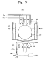
- FIG. 3 is a schematic diagram of a wafer dryer according to a preferred embodiment of the present invention.
- FIG. 4 is a top plan view of the wafer dryer shown in FIG. 3 .
- FIG. 5 is a diagram of a modified example of the wafer dryer according to the preferred embodiment of the present invention.
- a wafer dryer 200 for a semiconductor cleaning apparatus includes an internal bath 210 , an external bath 220 , a wafer guide 230 , a direction adjusting valve 250 , a solution supply line 260 , a solution drain line, a pump 290 , and drying means.
- the solution supply line 260 supplies a solution for cleaning and drying wafers to the internal bath 210 .
- the solution contained in the internal bath 210 overflows to be sent to external bath 220 .
- the overflowing solution is drained to the outside through a drain line (not shown).
- the wafer guide 230 for receiving a plurality of wafers is installed in the internal bath 210 .
- IPA is sprayed into a surface of the solution contained in the internal bath 210 from an IPA nozzle 310 that is one of the drying means.
- This method uses surface tensions of the DI water and the IPA.
- the solution having an IPA liquid film is slowly drained through the first drain line 270 .
- a valve 272 for adjusting the amount of the drained solution is stalled on the first drain line 270 .
- a pump 280 for constantly maintaining a solution drain speed is mounted upon the first drain line.
- the solution drain speed can be constantly maintained as compared to the prior art using the gravity.
- the solution drain speed can be converted by a speed converting device 290 for adjusting a rotation speed of the pump 280 .
- a speed converting device 290 for adjusting a rotation speed of the pump 280 .
- a plurality of gas spray nozzles 330 which are one of the drying means, are installed on the internal bath 210 and spray heated N 2 gas into the internal bath 210 to dry wafers. Until the solution is drained through the first drain line 270 , the first gas spray nozzles 330 do not spray the gas.
- the N 2 gas of normal temperature is sprayed to the external bath 220 through the second gas spray nozzle 320 . This is for eliminating oxygen in the wafer dryer 200 to prevent formation of an oxide layer at a wafer surface. As a result, no wave is created at a surface of the solution when the solution is drained through the first drain line 270 .
- the wafer dryer 200 has a direction adjusting valve 240 that is installed below the internal bath 210 and communicates therewith.
- the solution supply line 250 and the first and second drain lines 270 and 260 are connected to the direction adjusting valve 240 .
- the direction adjusting valve 240 is a tri-direction adjusting valve where one direction is opened and the other directions are closed. That is, in a case where the solution is supplied to the internal bath 210 through the solution drain line 250 , a connecting part of the direction adjusting valve 240 with the solution drain line 250 is opened to allow the solution to flow while connecting parts of the direction adjusting valve 240 with the first and second drain lines 270 and 260 are closed.
- the second gas spray nozzle 320 sprays N 2 gas of normal temperature to the external bath 220 so as to eliminate oxygen in the wafer dryer 200 .
- the second gas spray nozzle 320 is installed on four internal sidewalls of the external bath 220 , and has a plurality of holes for spraying gas to the external bath 220 .
- the gas is sprayed into the external bath 220 through the second gas spray nozzle 320 .
- no wave is produced at a surface of the drained solution.
- FIG. 5 A wafer dryer 400 without the direction adjusting valve (shown in FIG. 3) is illustrated in FIG. 5 .
- a solution supply line 440 , a first drain line 460 , and a second drain line 450 are independently connected to an internal bath 410 .
- a solution flow is adjusted by valves 442 , 462 , and 452 that are installed on the solution supply line 440 , the first drain line 460 , and the second drain line 450 , respectively.
- the wafer dryer 400 has the same components as explained in FIG. 3, so that they will not be explained in further detail.
- a speed of a drained solution is constantly maintained and adjusted to shorten a time required for drying wafers and to meet optimal drying process conditions for enhancing a quality to clean and dry the wafers.
- N 2 gas is not directly sprayed onto a solution surface when the solution is drained, no wave is produced at the solution surface. Therefore, it is possible to realize a stable environment for a cleaning process and a drying process.
Landscapes
- Cleaning Or Drying Semiconductors (AREA)
Abstract
Description
Claims (19)
Applications Claiming Priority (3)
| Application Number | Priority Date | Filing Date | Title |
|---|---|---|---|
| KR10-2001-0075657A KR100418324B1 (en) | 2001-12-01 | 2001-12-01 | Wafer dryer for semiconductor cleaning apparatus |
| KR2001-75657 | 2001-12-01 | ||
| KR10-2001-0075657 | 2001-12-01 |
Publications (2)
| Publication Number | Publication Date |
|---|---|
| US20030101618A1 US20030101618A1 (en) | 2003-06-05 |
| US6748672B2 true US6748672B2 (en) | 2004-06-15 |
Family
ID=19716532
Family Applications (1)
| Application Number | Title | Priority Date | Filing Date |
|---|---|---|---|
| US10/307,105 Expired - Fee Related US6748672B2 (en) | 2001-12-01 | 2002-11-27 | Wafer dryers for Semiconductor cleaning apparatuses |
Country Status (3)
| Country | Link |
|---|---|
| US (1) | US6748672B2 (en) |
| JP (1) | JP2003224104A (en) |
| KR (1) | KR100418324B1 (en) |
Cited By (3)
| Publication number | Priority date | Publication date | Assignee | Title |
|---|---|---|---|---|
| US20050067000A1 (en) * | 2003-09-30 | 2005-03-31 | Tokyo Electron Limited | Method and apparatus for dispensing a rinse solution on a substrate |
| US20160086793A1 (en) * | 2014-09-24 | 2016-03-24 | Infineon Technologies Ag | Method and a processing device for processing at least one carrier |
| CN110849127A (en) * | 2019-11-11 | 2020-02-28 | 兰泽(荆门)智能科技有限公司 | Rotary pulling-up wafer drying method |
Families Citing this family (4)
| Publication number | Priority date | Publication date | Assignee | Title |
|---|---|---|---|---|
| KR100493849B1 (en) * | 2002-09-30 | 2005-06-08 | 삼성전자주식회사 | Apparatus for drying a wafer |
| JP2008306104A (en) * | 2007-06-11 | 2008-12-18 | Elpida Memory Inc | Wet treatment apparatus and wet treatment method |
| TWM352764U (en) * | 2008-06-19 | 2009-03-11 | Scientech Corp | Constant temperature gas/liquid mixture generating system for using in wafer drying process |
| JP2024017656A (en) * | 2022-07-28 | 2024-02-08 | 株式会社Screenホールディングス | Substrate processing equipment |
Citations (5)
| Publication number | Priority date | Publication date | Assignee | Title |
|---|---|---|---|---|
| US5845660A (en) * | 1995-12-07 | 1998-12-08 | Tokyo Electron Limited | Substrate washing and drying apparatus, substrate washing method, and substrate washing apparatus |
| US5885360A (en) * | 1995-12-18 | 1999-03-23 | Lg Semicon Co., Ltd. | Semiconductor wafer cleaning apparatus |
| US6352083B1 (en) * | 1997-11-20 | 2002-03-05 | Dainippon Screen Mfg. Co., Ltd. | Substrate treating apparatus and substrate treating method |
| US6430840B1 (en) * | 2000-08-03 | 2002-08-13 | Samsung Electronics Co., Ltd. | Method of and apparatus for drying a wafer using isopropyl alcohol |
| US6510859B1 (en) * | 1999-07-15 | 2003-01-28 | Tokyo Electron Limited | Apparatus and method for cleaning and drying object |
Family Cites Families (6)
| Publication number | Priority date | Publication date | Assignee | Title |
|---|---|---|---|---|
| JP3585200B2 (en) * | 1997-03-31 | 2004-11-04 | 大日本スクリーン製造株式会社 | Substrate processing equipment |
| JPH10308378A (en) * | 1997-05-07 | 1998-11-17 | Kaijo Corp | Drying of substrate surface |
| KR19990031278A (en) * | 1997-10-10 | 1999-05-06 | 윤종용 | Vacuum pump with exhaust detection unit to detect the exhaust state of the gas |
| JP2000100773A (en) * | 1998-09-17 | 2000-04-07 | Seiko Epson Corp | Semiconductor device manufacturing method and semiconductor manufacturing apparatus |
| KR20000015814U (en) * | 1999-01-18 | 2000-08-16 | 김영환 | Semiconductor wafer dryer |
| JP3556583B2 (en) * | 2000-08-03 | 2004-08-18 | 株式会社半導体先端テクノロジーズ | Semiconductor substrate cleaning and drying equipment |
-
2001
- 2001-12-01 KR KR10-2001-0075657A patent/KR100418324B1/en not_active Expired - Fee Related
-
2002
- 2002-11-20 JP JP2002336977A patent/JP2003224104A/en active Pending
- 2002-11-27 US US10/307,105 patent/US6748672B2/en not_active Expired - Fee Related
Patent Citations (5)
| Publication number | Priority date | Publication date | Assignee | Title |
|---|---|---|---|---|
| US5845660A (en) * | 1995-12-07 | 1998-12-08 | Tokyo Electron Limited | Substrate washing and drying apparatus, substrate washing method, and substrate washing apparatus |
| US5885360A (en) * | 1995-12-18 | 1999-03-23 | Lg Semicon Co., Ltd. | Semiconductor wafer cleaning apparatus |
| US6352083B1 (en) * | 1997-11-20 | 2002-03-05 | Dainippon Screen Mfg. Co., Ltd. | Substrate treating apparatus and substrate treating method |
| US6510859B1 (en) * | 1999-07-15 | 2003-01-28 | Tokyo Electron Limited | Apparatus and method for cleaning and drying object |
| US6430840B1 (en) * | 2000-08-03 | 2002-08-13 | Samsung Electronics Co., Ltd. | Method of and apparatus for drying a wafer using isopropyl alcohol |
Cited By (5)
| Publication number | Priority date | Publication date | Assignee | Title |
|---|---|---|---|---|
| US20050067000A1 (en) * | 2003-09-30 | 2005-03-31 | Tokyo Electron Limited | Method and apparatus for dispensing a rinse solution on a substrate |
| US7431040B2 (en) * | 2003-09-30 | 2008-10-07 | Tokyo Electron Limited | Method and apparatus for dispensing a rinse solution on a substrate |
| US20160086793A1 (en) * | 2014-09-24 | 2016-03-24 | Infineon Technologies Ag | Method and a processing device for processing at least one carrier |
| US9799505B2 (en) * | 2014-09-24 | 2017-10-24 | Infineon Technologies Ag | Method and a processing device for processing at least one carrier |
| CN110849127A (en) * | 2019-11-11 | 2020-02-28 | 兰泽(荆门)智能科技有限公司 | Rotary pulling-up wafer drying method |
Also Published As
| Publication number | Publication date |
|---|---|
| JP2003224104A (en) | 2003-08-08 |
| US20030101618A1 (en) | 2003-06-05 |
| KR20030045247A (en) | 2003-06-11 |
| KR100418324B1 (en) | 2004-02-14 |
Similar Documents
| Publication | Publication Date | Title |
|---|---|---|
| US7718011B2 (en) | Apparatus for cleaning and drying substrates | |
| US7021319B2 (en) | Assisted rinsing in a single wafer cleaning process | |
| CN101465273B (en) | Wet-type etching method for reducing wafer surface blemish and device thereof | |
| US6905570B2 (en) | Apparatus for manufacturing integrated circuit device | |
| US6757989B2 (en) | Wafer drying apparatus | |
| KR100435808B1 (en) | Method of drying wafer and apparatus for the same | |
| US6748672B2 (en) | Wafer dryers for Semiconductor cleaning apparatuses | |
| KR100480588B1 (en) | Drying method of semiconductor device by using vacuum dryer | |
| US20050045208A1 (en) | Apparatus and method for cleaning semiconductor substrates | |
| JP3556583B2 (en) | Semiconductor substrate cleaning and drying equipment | |
| KR101078145B1 (en) | Apparatus and method for drying substrate | |
| US20220359233A1 (en) | Substrate processing apparatus and substrate processing method | |
| KR100436900B1 (en) | Apparatus for cleaning wafers | |
| KR100626363B1 (en) | Substrate drying device | |
| JP2000254603A (en) | Processing device and processing method | |
| KR20030095589A (en) | Method For Manufacturing Semiconductors | |
| KR0165321B1 (en) | Wet etching equipment | |
| TWI912606B (en) | Method and single wafer processing system for processing of semiconductor wafers | |
| TW200406833A (en) | Wafer dryers for semiconductor cleaning apparatuses | |
| KR100481157B1 (en) | Method and apparatus for drying a substrate | |
| KR20050023573A (en) | Method of cleaning and drying wafers | |
| KR19990085621A (en) | Semiconductor device manufacturing method | |
| KR100321546B1 (en) | Apparatus and method for chuck cleaning of transfer robot | |
| JP2000133629A (en) | Substrate processor and its method | |
| JPH1140531A (en) | Cleaning system, cleaning apparatus and cleaning method |
Legal Events
| Date | Code | Title | Description |
|---|---|---|---|
| AS | Assignment |
Owner name: DNS KOREA CO., LTD., KOREA, REPUBLIC OF Free format text: ASSIGNMENT OF ASSIGNORS INTEREST;ASSIGNORS:LEE, SUNG-HEE;LEE, SANG-WHA;REEL/FRAME:013537/0439;SIGNING DATES FROM 20021114 TO 20021120 |
|
| FEPP | Fee payment procedure |
Free format text: PAYOR NUMBER ASSIGNED (ORIGINAL EVENT CODE: ASPN); ENTITY STATUS OF PATENT OWNER: LARGE ENTITY |
|
| CC | Certificate of correction | ||
| AS | Assignment |
Owner name: SEMES CO. LTD., KOREA, REPUBLIC OF Free format text: CHANGE OF NAME;ASSIGNOR:DNS KOREA CO., LTD.;REEL/FRAME:016525/0023 Effective date: 20050310 |
|
| FEPP | Fee payment procedure |
Free format text: PAT HOLDER NO LONGER CLAIMS SMALL ENTITY STATUS, ENTITY STATUS SET TO UNDISCOUNTED (ORIGINAL EVENT CODE: STOL); ENTITY STATUS OF PATENT OWNER: LARGE ENTITY |
|
| REFU | Refund |
Free format text: REFUND - SURCHARGE, PETITION TO ACCEPT PYMT AFTER EXP, UNINTENTIONAL (ORIGINAL EVENT CODE: R2551); ENTITY STATUS OF PATENT OWNER: LARGE ENTITY |
|
| FPAY | Fee payment |
Year of fee payment: 4 |
|
| FPAY | Fee payment |
Year of fee payment: 8 |
|
| REMI | Maintenance fee reminder mailed | ||
| LAPS | Lapse for failure to pay maintenance fees | ||
| STCH | Information on status: patent discontinuation |
Free format text: PATENT EXPIRED DUE TO NONPAYMENT OF MAINTENANCE FEES UNDER 37 CFR 1.362 |
|
| STCH | Information on status: patent discontinuation |
Free format text: PATENT EXPIRED DUE TO NONPAYMENT OF MAINTENANCE FEES UNDER 37 CFR 1.362 |
|
| FP | Lapsed due to failure to pay maintenance fee |
Effective date: 20160615 |