US6700738B1 - Read/write head coil tap having upper and lower portions - Google Patents
Read/write head coil tap having upper and lower portions Download PDFInfo
- Publication number
- US6700738B1 US6700738B1 US09/810,819 US81081901A US6700738B1 US 6700738 B1 US6700738 B1 US 6700738B1 US 81081901 A US81081901 A US 81081901A US 6700738 B1 US6700738 B1 US 6700738B1
- Authority
- US
- United States
- Prior art keywords
- pole
- center tab
- coil
- thin film
- write
- Prior art date
- Legal status (The legal status is an assumption and is not a legal conclusion. Google has not performed a legal analysis and makes no representation as to the accuracy of the status listed.)
- Expired - Fee Related, expires
Links
Images


Classifications
-
- B—PERFORMING OPERATIONS; TRANSPORTING
- B82—NANOTECHNOLOGY
- B82Y—SPECIFIC USES OR APPLICATIONS OF NANOSTRUCTURES; MEASUREMENT OR ANALYSIS OF NANOSTRUCTURES; MANUFACTURE OR TREATMENT OF NANOSTRUCTURES
- B82Y25/00—Nanomagnetism, e.g. magnetoimpedance, anisotropic magnetoresistance, giant magnetoresistance or tunneling magnetoresistance
-
- G—PHYSICS
- G11—INFORMATION STORAGE
- G11B—INFORMATION STORAGE BASED ON RELATIVE MOVEMENT BETWEEN RECORD CARRIER AND TRANSDUCER
- G11B5/00—Recording by magnetisation or demagnetisation of a record carrier; Reproducing by magnetic means; Record carriers therefor
- G11B5/127—Structure or manufacture of heads, e.g. inductive
- G11B5/31—Structure or manufacture of heads, e.g. inductive using thin films
- G11B5/3103—Structure or manufacture of integrated heads or heads mechanically assembled and electrically connected to a support or housing
-
- B—PERFORMING OPERATIONS; TRANSPORTING
- B82—NANOTECHNOLOGY
- B82Y—SPECIFIC USES OR APPLICATIONS OF NANOSTRUCTURES; MEASUREMENT OR ANALYSIS OF NANOSTRUCTURES; MANUFACTURE OR TREATMENT OF NANOSTRUCTURES
- B82Y10/00—Nanotechnology for information processing, storage or transmission, e.g. quantum computing or single electron logic
-
- G—PHYSICS
- G11—INFORMATION STORAGE
- G11B—INFORMATION STORAGE BASED ON RELATIVE MOVEMENT BETWEEN RECORD CARRIER AND TRANSDUCER
- G11B5/00—Recording by magnetisation or demagnetisation of a record carrier; Reproducing by magnetic means; Record carriers therefor
- G11B5/127—Structure or manufacture of heads, e.g. inductive
- G11B5/31—Structure or manufacture of heads, e.g. inductive using thin films
- G11B5/3109—Details
- G11B5/313—Disposition of layers
- G11B5/3133—Disposition of layers including layers not usually being a part of the electromagnetic transducer structure and providing additional features, e.g. for improving heat radiation, reduction of power dissipation, adaptations for measurement or indication of gap depth or other properties of the structure
-
- G—PHYSICS
- G11—INFORMATION STORAGE
- G11B—INFORMATION STORAGE BASED ON RELATIVE MOVEMENT BETWEEN RECORD CARRIER AND TRANSDUCER
- G11B5/00—Recording by magnetisation or demagnetisation of a record carrier; Reproducing by magnetic means; Record carriers therefor
- G11B5/127—Structure or manufacture of heads, e.g. inductive
- G11B5/33—Structure or manufacture of flux-sensitive heads, i.e. for reproduction only; Combination of such heads with means for recording or erasing only
- G11B5/39—Structure or manufacture of flux-sensitive heads, i.e. for reproduction only; Combination of such heads with means for recording or erasing only using magneto-resistive devices or effects
- G11B2005/3996—Structure or manufacture of flux-sensitive heads, i.e. for reproduction only; Combination of such heads with means for recording or erasing only using magneto-resistive devices or effects large or giant magnetoresistive effects [GMR], e.g. as generated in spin-valve [SV] devices
-
- G—PHYSICS
- G11—INFORMATION STORAGE
- G11B—INFORMATION STORAGE BASED ON RELATIVE MOVEMENT BETWEEN RECORD CARRIER AND TRANSDUCER
- G11B5/00—Recording by magnetisation or demagnetisation of a record carrier; Reproducing by magnetic means; Record carriers therefor
- G11B5/127—Structure or manufacture of heads, e.g. inductive
- G11B5/33—Structure or manufacture of flux-sensitive heads, i.e. for reproduction only; Combination of such heads with means for recording or erasing only
- G11B5/332—Structure or manufacture of flux-sensitive heads, i.e. for reproduction only; Combination of such heads with means for recording or erasing only using thin films
-
- G—PHYSICS
- G11—INFORMATION STORAGE
- G11B—INFORMATION STORAGE BASED ON RELATIVE MOVEMENT BETWEEN RECORD CARRIER AND TRANSDUCER
- G11B5/00—Recording by magnetisation or demagnetisation of a record carrier; Reproducing by magnetic means; Record carriers therefor
- G11B5/127—Structure or manufacture of heads, e.g. inductive
- G11B5/33—Structure or manufacture of flux-sensitive heads, i.e. for reproduction only; Combination of such heads with means for recording or erasing only
- G11B5/39—Structure or manufacture of flux-sensitive heads, i.e. for reproduction only; Combination of such heads with means for recording or erasing only using magneto-resistive devices or effects
- G11B5/3903—Structure or manufacture of flux-sensitive heads, i.e. for reproduction only; Combination of such heads with means for recording or erasing only using magneto-resistive devices or effects using magnetic thin film layers or their effects, the films being part of integrated structures
- G11B5/3967—Composite structural arrangements of transducers, e.g. inductive write and magnetoresistive read
Definitions
- the present invention relates in general to data storage systems such as disk drives, and it particularly relates to a thin film read/write head for use in such data storage systems. More specifically, the present invention relates to a thin film, inductive-type advanced read/write head with a single layer coil and an improved method of fabricating a center tab of the single layer coil.
- a thin film magnetic head in a conventional magnetic storage system, includes an inductive read/write element mounted on a slider.
- the magnetic head is coupled to a rotary actuator magnet and a voice coil assembly by a suspension and an actuator arm positioned over a surface of a spinning magnetic disk.
- a lift force is generated by the aerodynamic interaction between the magnetic head and the spinning magnetic disk.
- the lift force is opposed by equal and opposite spring forces applied by the suspension such that a predetermined flying height is maintained over a full radial stroke of the rotary actuator assembly above the surface of the spinning magnetic disk.
- An exemplary magnetic head includes a thin film write head with a bottom pole (P 1 ) and a top pole (P 2 ).
- the poles P 1 and P 2 have a pole tip height dimension commonly referred to as “throat height”.
- the throat height is measured between an air bearing surface (“ABS”), formed by lapping and polishing the pole tip, and a zero throat level where the pole tip of the write head transitions to a back region.
- a pole tip region is defined as the region between the ABS and the zero throat level.
- Each of the poles P 1 and P 2 has a pole tip located in the pole tip region. The tip regions of the poles P 1 and P 2 are separated by a magnetic recording gap, which is a thin layer of insulation material.
- a center tab 2 is formed typically after the main coil body 3 , the insulating layer 4 , and the P 2 pole have been formed. As a result, the coil resistance and inductance of the write head cannot be readily monitored once the coil fabrication is completed.
- center tab process requires several wafer processing steps such as target window seed removal (photolithography and wet etch), center tab fabrication (photolithography, plating, and wet etch of seed), and so forth.
- One aspect of the present invention is to satisfy the long felt, and still unsatisfied need for a thin film read/write head with a single layer coil, and an improved fabrication process of the center tab of the single layer coil that reduces the complexity of the wafer processing, which would result in a shorter cycle time as demanded by the need for a faster design-to-market cycle.
- the center tab is formed prior to the fabrication of the coil main body, the insulating layer, and the pole P 2 .
- This new fabrication method increases the manufacturing yield and eliminates several wafer processing steps, thereby significantly reducing the cycle time of wafer processing.
- FIG. 1 is a fragmentary perspective view of a data storage system utilizing a read/write head according to the invention
- FIG. 2 is a perspective view of a head gimbal assembly comprised of a suspension, and a slider to which the read/write head of the present invention is secured, for use in a head stack assembly;
- FIG. 3 is an enlarged perspective view of a thin film read/write element (with the top yoke removed for clarity of illustration) forming part of the read/write head of FIGS. 1 and 2, and made according to the present invention;
- FIG. 4 is a cross-sectional, partly fragmentary view of a conventional write head (without the read element), shown positioned relative to a data storage medium;
- FIG. 5 is a cross-sectional, partly fragmentary view of the write head (with the read element not included) of FIG. 3 taken along line 4 - 4 , and shown positioned relative to the data storage medium;
- FIGS. 6A through 6H are schematic, side view illustrations of a sequence of steps implemented in the fabrication of the thin film write head of FIGS. 3 and 5;
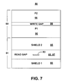
- FIG. 7 is an ABS view of the read/write head of the present invention. Similar numerals in the drawings refer to similar elements. It should be understood that the sizes of the different components in the figures might not be in exact proportion, and are shown for visual clarity and for the purpose of explanation.
- FIG. 1 illustrates a disk drive 10 comprised of a head stack assembly 12 and a stack of spaced apart magnetic data storage disks or media 14 that rotate about a common shaft 15 .
- the head stack assembly 12 is pivoted about an actuator axis 16 in the direction of the arrow C.
- the head stack assembly 12 includes a number of actuator arms, only three of which 18 A, 18 B, 18 C are illustrated, which extend into spacings between the disks 14 .
- the head stack assembly 12 further includes an E-shaped block 19 and a magnetic rotor 20 attached to the block 19 in a position diametrically opposite to the actuator arms 18 A, 18 B, 18 C.
- the rotor 20 cooperates with a stator for rotating in an arc about the actuator axis 16 .
- Energizing a coil of the rotor 20 with a direct current in one polarity or the reverse polarity causes the head stack assembly 12 , including the actuator arms 18 A, 18 B, 18 C, to rotate about the actuator axis 16 in a direction substantially radial to the disks 14 .
- a head gimbal assembly (HGA) 28 is secured to each of the actuator arms, for instance 18 A.
- the HGA 28 is comprised of a suspension 33 and a read/write head 35 .
- the suspension 33 includes a resilient load beam 36 and a flexure 40 to which the head 35 is secured.
- the head 35 is formed of a slider 47 secured to the free end of the load beam 36 by means of the flexure 40 , and a read/write element 50 supported by the slider 47 .
- the read/write element 50 is secured to the trailing edge 55 of the slider 47 .
- the slider 47 can be any conventional or available slider.
- the read/write element 50 integrates a write section 60 and a read section 61 .
- the read section 61 is formed of a first shield layer (Shield 1 ) 80 preferably made of a material that is both magnetically and electrically conductive.
- the first shield layer 80 can have a nickel-iron (NiFe) composition, such as Permalloy, or a ferromagnetic composition with high permeability.
- the thickness of the first shield layer 80 can be in the range of approximately 0.5 micron to approximately 14 microns.
- An insulating layer 82 is formed over substantially the entire surface of the first shield layer 80 to define a non-magnetic, transducing read gap 87 .
- the insulation layer can be made of any suitable material, for example alumina (Al 2 O 3 ), aluminum oxide or silicon nitride.
- the read section 61 is also comprised of a read sensor 83 formed within the insulation layer 82 .
- the read sensor 83 can be any suitable sensor, including but not limited to a magnetoresistive (MR) element, a giant magnetoresistive (GMR) element, a spin valve, or a Current In the Plane mode (CIP) sensor.
- MR magnetoresistive
- GMR giant magnetoresistive
- CIP Current In the Plane mode
- a GMR element can be formed, by way of example, by depositing a plurality of alternating ultra-thin layers of magnetically conductive and nonconductive materials such as Permalloy (Ni80 Fe20) and copper (Cu), each layer being approximately 10 to 30 angstroms thick.
- the electric resistance of the GMR element 83 fluctuates when exposed to a time-varying magnetic flux.
- a magnetoresistive element is sensitive to the magnitude of a flux transition rather than to the rate of change of the flux transition. This gives the magnetoresistive element 83 certain advantages over inductive transducers, such as insensitivity to disk speed changes.
- the overall thickness of the GMR element 83 can be in the range of approximately 30 angstroms to approximately 3000 angstroms.
- the read section 61 is also comprised of a second shield layer (Shield 2 ) 85 that is made of an electrically and magnetically conductive material, which may be similar or equivalent to that of the first shield layer 80 .
- the second shield layer 85 is formed over substantially the entire surface of the insulating layer 82 , and has a thickness that can be substantially similar or equivalent to that of the first shield layer 80 .
- the second shield layer 85 terminates at a sloped back edge 120 .
- a read circuit 102 (not shown) is connected to the first shield layer 80 and the second shield layer 85 , such that during a read mode the read circuit sends a sensing electric current I R through the sensor 83 and the second shield layer 85 .
- the read-sense current I R flows perpendicularly through the sensor 83 , thus avoiding the along-the plane electromigration problems and magnetic-biasing due to parallel-current problems associated with earlier designs based on CIP operation (Current In the Plane mode).
- CIP operation Current In the Plane mode
- the write section 60 is comprised of a first pole layer or pedestal P 1 (also referenced by the numeral 90 ) that extends, for example, integrally from the second shield layer 85 .
- the pedestal P 1 includes a back edge 92 that defines the zero throat level with extreme accuracy. In a preferred embodiment, the pedestal P 1 extends only to the zero throat 92 .
- a write coil 135 includes a plurality of a plurality of conductive coil elements (or conductors) 135 A, only a few of which are illustrated and also form part of the write section 60 .
- the coil elements 135 A are formed within an insulating layer 95 .
- the single layer write coil 135 can preferably have, for example, 1 to 30 turns, though a different number of turns can alternatively be selected depending on the application or design.
- a second pole layer 96 is made of a magnetically conductive material, and be for example only, similar or equivalent to that of the first shield layer 80 and the first pole layer 85 .
- the second pole layer 96 is formed over, and is separated from the pedestal 90 , to define a write gap 114 therewith.
- the thickness of the second pole layer 96 can be substantially the same as, or similar to that of the first shield layer 80 .
- the write gap 114 can be filled with a material similar or equivalent to that of the insulating layer 82 .
- the second pole layer 96 includes an edge 115 along which the second pole layer 96 is stitched to a top (or upper) yoke 104 .
- the yoke 104 covers substantially the entire surface of the write coil 135 and a back gap region 125 , and terminates at a forward-facing curved apex region 130 .
- a write circuit 100 (not shown) is connected to the write coil 135 , and, during a write mode, it sends an electrical current I W to induce a flux flow through the write gap 114 . Changes in the flux flow across the write gap 114 produce the different magnetic orientations of magnetized regions or domains in the disk 14 during a write operation.
- An insulating layer 11 (also referenced by the numeral 112 ) is deposited between the write gap 114 and the second shield layer 85 , and extends from the pedestal P 1 back edge 92 over substantially the entire length of the write coil 135 .
- the insulating layer 11 is made of insulating material, which may be similar or equivalent to that of the insulating layer 82 .
- the thickness of the insulating layer 11 can be substantially the same as that of the pedestal P 1 .
- the single layer coil 135 includes a plurality of multi-turned conductive coil elements (or conductors) 135 A, only a few of which are illustrated for the purpose of clarity.
- the coil elements 135 A are formed within an insulating layer 140 .
- a region intermediate to the write coil 135 and a single layer coil 135 is referred to as a back gap region 125 .
- the back gap region 125 is formed substantially by an electrically and magnetically conductive material, which may be similar or equivalent to that of the second shield layer 85 .
- An insulating layer 12 (also referenced by the numeral 145 ) is formed over substantially the entire length of the single layer coil 135 , starting at the sloped back edge 120 of the second shield layer 85 .
- Another insulating layer 150 is immediately deposited on top of the insulating layer 12 over substantially the entire length of the single layer coil 135 .
- a center tab 160 is embedded in the insulating layers 12 and 150 and electrically connects to the single layer coil 135 .
- An upper portion 165 of the center tab 160 is formed within the insulating layer 140 of the single layer coil 135 .
- a lower portion 170 of the center tab 160 extends from the single layer coil 135 through the insulating layers 12 and 150 .
- a bottom edge 175 of the lower portion 170 is formed flush with a lower surface 176 of the insulation layer 12 .
- An opening 180 in the write gap 114 is referred to as a lead via.
- the center tab 160 provides electrical connection to the single layer coil 135 .
- the second shield layer 85 is formed using known or available thin film deposition techniques.
- the next step is illustrated in FIG. 6B, where a portion 110 (shown in dotted lines) of the second shield layer 85 , is milled away to form the pedestal P 1 , and to define the back edge 92 with great precision.
- the pedestal P 1 can be formed using pattern plating techniques, which would also form the zero throat level with great precision.
- the back edge 92 defines the zero throat level of the read/write head 35 .
- the zero throat level (also referenced herein by the numeral 92 ) lies in a well defined plane that is generally parallel to the plane of the air bearing surface (“ABS”) level, which, in turn, is co-planar with the forward edge of the pedestal P 1 .
- the pole tip region of the read/write head 35 is defined as the region between the zero throat level and the ABS level.
- the next step is to form the center tab 160 together with electrical interconnects for the read element 83 onto the write section 60 at the trailing edge of the second shield layer 85 .
- the center tab 160 is located, in such a manner that the lower edge 175 of the lower portion 170 (FIG. 5) is co-planar with the lower surface 177 of the second shield layer 85 .
- an insulating layer 112 (or 11 ) is deposited on the second shield layer 85 , within the region 110 that has been milled away to define the pedestal P 1 (FIG. 6 B).
- FIG. 6C shows the insulating layer 112 as having been lapped to the same height as that of the pedestal P 1 .
- the back edge 92 of the pedestal P 1 is shown in dotted lines as it is actually covered by the insulating layer 112 , the back edge 92 will be represented by a solid line in subsequent FIGS. 6D through 6H for the purpose of clarity.
- FIG. 6D complements FIG. 6 C and illustrates an intermediary manufacturing step, prior to the lapping of the insulating layer 112 , namely, the patterning of the lower portion 170 of the center tab 160 .
- the advantage of forming the center tab 160 with the interconnects at this stage for the read element 83 is that several conventional wafer processing steps can now be eliminated, thereby significantly reducing the cycle time of wafer processing.
- the insulating layer 150 can be processed concurrently with the insulating layer 112 , and is deposited and lapped to maintain a flat surface that is substantially flush with the upper portion 170 A of the center tab 160 .
- the next fabrication step is illustrated in FIG. 6E, wherein the write gap 114 is formed by depositing a thin, uniform, write gap 114 that separates the pedestal P 1 from the top pole P 2 ( 96 ).
- the write gap 114 covers substantially the entire surface of the pedestal P 1 and the insulating layer 112 .
- the thickness of the write gap 114 ranges between approximately 100 Angstroms and 10000 Angstroms, with the preferred range being 500 Angstroms and 2000 Angstroms.
- the write gap 114 is formed next by depositing a thin, uniform, insulating layer 190 that separates the insulating layer 150 from the single layer coil 135 .
- the next fabrication step is illustrated in FIG. 6F, wherein the lead via 180 is formed by chemical etch.
- the write coil 135 comprised of the conductor elements 1 35 A and the insulating layer 95 , is formed on the write gap 114 at a distance from the second pole layer P 2 ( 96 ).
- the top pole P 2 ( 96 ) is formed by depositing a film of magnetic material by means of known or available techniques, such as sputter deposition and etching, or pattern plating. After the top pole P 2 is formed, it is etched or milled (using available or known techniques) such that the pattern of the top pole P 2 is etched into the pedestal P 1 .
- the fabrication process described herein will enable the single layer coil ( 135 ) resistance and inductance to be monitored for all the devices in wafer immediately after the coil fabrication, since the center tab 160 is formed before the conductor elements 135 A of the single layer coil 135 is formed.
- the ability to monitor the coil resistance and inductance allow the manufacturer to screen defects in the manufacture process before final production, thereby improving yield by identifying additional processing or rework (such as coil seed removal) if necessary.
- the number of processing steps will also be reduced and therefore the manufacturing cycle time of wafer processing will be significantly shortened because the center tab 170 is processed concurrently with the interconnect, e.g. a lead that connects the read element 83 to a read circuit (not shown).
Landscapes
- Engineering & Computer Science (AREA)
- Chemical & Material Sciences (AREA)
- Nanotechnology (AREA)
- Manufacturing & Machinery (AREA)
- Crystallography & Structural Chemistry (AREA)
- Physics & Mathematics (AREA)
- Mathematical Physics (AREA)
- Theoretical Computer Science (AREA)
- Electromagnetism (AREA)
- Magnetic Heads (AREA)
Abstract
Description
Claims (10)
Priority Applications (1)
| Application Number | Priority Date | Filing Date | Title |
|---|---|---|---|
| US09/810,819 US6700738B1 (en) | 2001-03-16 | 2001-03-16 | Read/write head coil tap having upper and lower portions |
Applications Claiming Priority (1)
| Application Number | Priority Date | Filing Date | Title |
|---|---|---|---|
| US09/810,819 US6700738B1 (en) | 2001-03-16 | 2001-03-16 | Read/write head coil tap having upper and lower portions |
Publications (1)
| Publication Number | Publication Date |
|---|---|
| US6700738B1 true US6700738B1 (en) | 2004-03-02 |
Family
ID=31716227
Family Applications (1)
| Application Number | Title | Priority Date | Filing Date |
|---|---|---|---|
| US09/810,819 Expired - Fee Related US6700738B1 (en) | 2001-03-16 | 2001-03-16 | Read/write head coil tap having upper and lower portions |
Country Status (1)
| Country | Link |
|---|---|
| US (1) | US6700738B1 (en) |
Cited By (132)
| Publication number | Priority date | Publication date | Assignee | Title |
|---|---|---|---|---|
| US20050286169A1 (en) * | 2004-06-29 | 2005-12-29 | Amanda Baer | Slider with underpass leads and methods of fabrication |
| US7493688B1 (en) * | 2006-02-13 | 2009-02-24 | Western Digital (Fremont), Llc | Method of manufacturing a magnetic recording transducer |
| US8830628B1 (en) | 2009-02-23 | 2014-09-09 | Western Digital (Fremont), Llc | Method and system for providing a perpendicular magnetic recording head |
| US8879207B1 (en) | 2011-12-20 | 2014-11-04 | Western Digital (Fremont), Llc | Method for providing a side shield for a magnetic recording transducer using an air bridge |
| US8883017B1 (en) | 2013-03-12 | 2014-11-11 | Western Digital (Fremont), Llc | Method and system for providing a read transducer having seamless interfaces |
| US8917581B1 (en) | 2013-12-18 | 2014-12-23 | Western Digital Technologies, Inc. | Self-anneal process for a near field transducer and chimney in a hard disk drive assembly |
| US8923102B1 (en) | 2013-07-16 | 2014-12-30 | Western Digital (Fremont), Llc | Optical grating coupling for interferometric waveguides in heat assisted magnetic recording heads |
| US8947985B1 (en) | 2013-07-16 | 2015-02-03 | Western Digital (Fremont), Llc | Heat assisted magnetic recording transducers having a recessed pole |
| US8953422B1 (en) | 2014-06-10 | 2015-02-10 | Western Digital (Fremont), Llc | Near field transducer using dielectric waveguide core with fine ridge feature |
| US8958272B1 (en) | 2014-06-10 | 2015-02-17 | Western Digital (Fremont), Llc | Interfering near field transducer for energy assisted magnetic recording |
| US8971160B1 (en) | 2013-12-19 | 2015-03-03 | Western Digital (Fremont), Llc | Near field transducer with high refractive index pin for heat assisted magnetic recording |
| US8970988B1 (en) | 2013-12-31 | 2015-03-03 | Western Digital (Fremont), Llc | Electric gaps and method for making electric gaps for multiple sensor arrays |
| US8976635B1 (en) | 2014-06-10 | 2015-03-10 | Western Digital (Fremont), Llc | Near field transducer driven by a transverse electric waveguide for energy assisted magnetic recording |
| US8980109B1 (en) | 2012-12-11 | 2015-03-17 | Western Digital (Fremont), Llc | Method for providing a magnetic recording transducer using a combined main pole and side shield CMP for a wraparound shield scheme |
| US8982508B1 (en) | 2011-10-31 | 2015-03-17 | Western Digital (Fremont), Llc | Method for providing a side shield for a magnetic recording transducer |
| US8988812B1 (en) | 2013-11-27 | 2015-03-24 | Western Digital (Fremont), Llc | Multi-sensor array configuration for a two-dimensional magnetic recording (TDMR) operation |
| US8988825B1 (en) | 2014-02-28 | 2015-03-24 | Western Digital (Fremont, LLC | Method for fabricating a magnetic writer having half-side shields |
| US8984740B1 (en) | 2012-11-30 | 2015-03-24 | Western Digital (Fremont), Llc | Process for providing a magnetic recording transducer having a smooth magnetic seed layer |
| US8993217B1 (en) | 2013-04-04 | 2015-03-31 | Western Digital (Fremont), Llc | Double exposure technique for high resolution disk imaging |
| US8995087B1 (en) | 2006-11-29 | 2015-03-31 | Western Digital (Fremont), Llc | Perpendicular magnetic recording write head having a wrap around shield |
| US9001467B1 (en) | 2014-03-05 | 2015-04-07 | Western Digital (Fremont), Llc | Method for fabricating side shields in a magnetic writer |
| US8997832B1 (en) | 2010-11-23 | 2015-04-07 | Western Digital (Fremont), Llc | Method of fabricating micrometer scale components |
| US9001628B1 (en) | 2013-12-16 | 2015-04-07 | Western Digital (Fremont), Llc | Assistant waveguides for evaluating main waveguide coupling efficiency and diode laser alignment tolerances for hard disk |
| US9007879B1 (en) | 2014-06-10 | 2015-04-14 | Western Digital (Fremont), Llc | Interfering near field transducer having a wide metal bar feature for energy assisted magnetic recording |
| US9007725B1 (en) | 2014-10-07 | 2015-04-14 | Western Digital (Fremont), Llc | Sensor with positive coupling between dual ferromagnetic free layer laminates |
| US9007719B1 (en) | 2013-10-23 | 2015-04-14 | Western Digital (Fremont), Llc | Systems and methods for using double mask techniques to achieve very small features |
| US9013836B1 (en) | 2013-04-02 | 2015-04-21 | Western Digital (Fremont), Llc | Method and system for providing an antiferromagnetically coupled return pole |
| US9042058B1 (en) | 2013-10-17 | 2015-05-26 | Western Digital Technologies, Inc. | Shield designed for middle shields in a multiple sensor array |
| US9042052B1 (en) | 2014-06-23 | 2015-05-26 | Western Digital (Fremont), Llc | Magnetic writer having a partially shunted coil |
| US9042051B2 (en) | 2013-08-15 | 2015-05-26 | Western Digital (Fremont), Llc | Gradient write gap for perpendicular magnetic recording writer |
| US9042208B1 (en) | 2013-03-11 | 2015-05-26 | Western Digital Technologies, Inc. | Disk drive measuring fly height by applying a bias voltage to an electrically insulated write component of a head |
| US9042057B1 (en) | 2013-01-09 | 2015-05-26 | Western Digital (Fremont), Llc | Methods for providing magnetic storage elements with high magneto-resistance using Heusler alloys |
| US9053735B1 (en) | 2014-06-20 | 2015-06-09 | Western Digital (Fremont), Llc | Method for fabricating a magnetic writer using a full-film metal planarization |
| US9064528B1 (en) | 2013-05-17 | 2015-06-23 | Western Digital Technologies, Inc. | Interferometric waveguide usable in shingled heat assisted magnetic recording in the absence of a near-field transducer |
| US9065043B1 (en) | 2012-06-29 | 2015-06-23 | Western Digital (Fremont), Llc | Tunnel magnetoresistance read head with narrow shield-to-shield spacing |
| US9064507B1 (en) | 2009-07-31 | 2015-06-23 | Western Digital (Fremont), Llc | Magnetic etch-stop layer for magnetoresistive read heads |
| US9064527B1 (en) | 2013-04-12 | 2015-06-23 | Western Digital (Fremont), Llc | High order tapered waveguide for use in a heat assisted magnetic recording head |
| US9070381B1 (en) | 2013-04-12 | 2015-06-30 | Western Digital (Fremont), Llc | Magnetic recording read transducer having a laminated free layer |
| US9082423B1 (en) | 2013-12-18 | 2015-07-14 | Western Digital (Fremont), Llc | Magnetic recording write transducer having an improved trailing surface profile |
| US9087534B1 (en) | 2011-12-20 | 2015-07-21 | Western Digital (Fremont), Llc | Method and system for providing a read transducer having soft and hard magnetic bias structures |
| US9087527B1 (en) | 2014-10-28 | 2015-07-21 | Western Digital (Fremont), Llc | Apparatus and method for middle shield connection in magnetic recording transducers |
| US9093639B2 (en) | 2012-02-21 | 2015-07-28 | Western Digital (Fremont), Llc | Methods for manufacturing a magnetoresistive structure utilizing heating and cooling |
| US9104107B1 (en) | 2013-04-03 | 2015-08-11 | Western Digital (Fremont), Llc | DUV photoresist process |
| US9111564B1 (en) | 2013-04-02 | 2015-08-18 | Western Digital (Fremont), Llc | Magnetic recording writer having a main pole with multiple flare angles |
| US9111550B1 (en) | 2014-12-04 | 2015-08-18 | Western Digital (Fremont), Llc | Write transducer having a magnetic buffer layer spaced between a side shield and a write pole by non-magnetic layers |
| US9111558B1 (en) | 2014-03-14 | 2015-08-18 | Western Digital (Fremont), Llc | System and method of diffractive focusing of light in a waveguide |
| US9123374B1 (en) | 2015-02-12 | 2015-09-01 | Western Digital (Fremont), Llc | Heat assisted magnetic recording writer having an integrated polarization rotation plate |
| US9123358B1 (en) | 2012-06-11 | 2015-09-01 | Western Digital (Fremont), Llc | Conformal high moment side shield seed layer for perpendicular magnetic recording writer |
| US9123362B1 (en) | 2011-03-22 | 2015-09-01 | Western Digital (Fremont), Llc | Methods for assembling an electrically assisted magnetic recording (EAMR) head |
| US9123359B1 (en) | 2010-12-22 | 2015-09-01 | Western Digital (Fremont), Llc | Magnetic recording transducer with sputtered antiferromagnetic coupling trilayer between plated ferromagnetic shields and method of fabrication |
| US9135937B1 (en) | 2014-05-09 | 2015-09-15 | Western Digital (Fremont), Llc | Current modulation on laser diode for energy assisted magnetic recording transducer |
| US9135930B1 (en) | 2014-03-06 | 2015-09-15 | Western Digital (Fremont), Llc | Method for fabricating a magnetic write pole using vacuum deposition |
| US9142233B1 (en) | 2014-02-28 | 2015-09-22 | Western Digital (Fremont), Llc | Heat assisted magnetic recording writer having a recessed pole |
| US9147404B1 (en) | 2015-03-31 | 2015-09-29 | Western Digital (Fremont), Llc | Method and system for providing a read transducer having a dual free layer |
| US9147408B1 (en) | 2013-12-19 | 2015-09-29 | Western Digital (Fremont), Llc | Heated AFM layer deposition and cooling process for TMR magnetic recording sensor with high pinning field |
| US9153255B1 (en) | 2014-03-05 | 2015-10-06 | Western Digital (Fremont), Llc | Method for fabricating a magnetic writer having an asymmetric gap and shields |
| US9183854B2 (en) | 2014-02-24 | 2015-11-10 | Western Digital (Fremont), Llc | Method to make interferometric taper waveguide for HAMR light delivery |
| US9190079B1 (en) | 2014-09-22 | 2015-11-17 | Western Digital (Fremont), Llc | Magnetic write pole having engineered radius of curvature and chisel angle profiles |
| US9190085B1 (en) | 2014-03-12 | 2015-11-17 | Western Digital (Fremont), Llc | Waveguide with reflective grating for localized energy intensity |
| US9194692B1 (en) | 2013-12-06 | 2015-11-24 | Western Digital (Fremont), Llc | Systems and methods for using white light interferometry to measure undercut of a bi-layer structure |
| US9202493B1 (en) | 2014-02-28 | 2015-12-01 | Western Digital (Fremont), Llc | Method of making an ultra-sharp tip mode converter for a HAMR head |
| US9202480B2 (en) | 2009-10-14 | 2015-12-01 | Western Digital (Fremont), LLC. | Double patterning hard mask for damascene perpendicular magnetic recording (PMR) writer |
| US9213322B1 (en) | 2012-08-16 | 2015-12-15 | Western Digital (Fremont), Llc | Methods for providing run to run process control using a dynamic tuner |
| US9214172B2 (en) | 2013-10-23 | 2015-12-15 | Western Digital (Fremont), Llc | Method of manufacturing a magnetic read head |
| US9214169B1 (en) | 2014-06-20 | 2015-12-15 | Western Digital (Fremont), Llc | Magnetic recording read transducer having a laminated free layer |
| US9214165B1 (en) | 2014-12-18 | 2015-12-15 | Western Digital (Fremont), Llc | Magnetic writer having a gradient in saturation magnetization of the shields |
| US9230565B1 (en) | 2014-06-24 | 2016-01-05 | Western Digital (Fremont), Llc | Magnetic shield for magnetic recording head |
| US9236560B1 (en) | 2014-12-08 | 2016-01-12 | Western Digital (Fremont), Llc | Spin transfer torque tunneling magnetoresistive device having a laminated free layer with perpendicular magnetic anisotropy |
| US9245562B1 (en) | 2015-03-30 | 2016-01-26 | Western Digital (Fremont), Llc | Magnetic recording writer with a composite main pole |
| US9245545B1 (en) | 2013-04-12 | 2016-01-26 | Wester Digital (Fremont), Llc | Short yoke length coils for magnetic heads in disk drives |
| US9245543B1 (en) | 2010-06-25 | 2016-01-26 | Western Digital (Fremont), Llc | Method for providing an energy assisted magnetic recording head having a laser integrally mounted to the slider |
| US9251813B1 (en) | 2009-04-19 | 2016-02-02 | Western Digital (Fremont), Llc | Method of making a magnetic recording head |
| US9263067B1 (en) | 2013-05-29 | 2016-02-16 | Western Digital (Fremont), Llc | Process for making PMR writer with constant side wall angle |
| US9263071B1 (en) | 2015-03-31 | 2016-02-16 | Western Digital (Fremont), Llc | Flat NFT for heat assisted magnetic recording |
| US9269382B1 (en) | 2012-06-29 | 2016-02-23 | Western Digital (Fremont), Llc | Method and system for providing a read transducer having improved pinning of the pinned layer at higher recording densities |
| US9275657B1 (en) | 2013-08-14 | 2016-03-01 | Western Digital (Fremont), Llc | Process for making PMR writer with non-conformal side gaps |
| US9280990B1 (en) | 2013-12-11 | 2016-03-08 | Western Digital (Fremont), Llc | Method for fabricating a magnetic writer using multiple etches |
| US9287494B1 (en) | 2013-06-28 | 2016-03-15 | Western Digital (Fremont), Llc | Magnetic tunnel junction (MTJ) with a magnesium oxide tunnel barrier |
| US9286919B1 (en) | 2014-12-17 | 2016-03-15 | Western Digital (Fremont), Llc | Magnetic writer having a dual side gap |
| US9305583B1 (en) | 2014-02-18 | 2016-04-05 | Western Digital (Fremont), Llc | Method for fabricating a magnetic writer using multiple etches of damascene materials |
| US9312064B1 (en) | 2015-03-02 | 2016-04-12 | Western Digital (Fremont), Llc | Method to fabricate a magnetic head including ion milling of read gap using dual layer hard mask |
| US9318130B1 (en) | 2013-07-02 | 2016-04-19 | Western Digital (Fremont), Llc | Method to fabricate tunneling magnetic recording heads with extended pinned layer |
| US9336814B1 (en) | 2013-03-12 | 2016-05-10 | Western Digital (Fremont), Llc | Inverse tapered waveguide for use in a heat assisted magnetic recording head |
| US9343086B1 (en) | 2013-09-11 | 2016-05-17 | Western Digital (Fremont), Llc | Magnetic recording write transducer having an improved sidewall angle profile |
| US9343087B1 (en) | 2014-12-21 | 2016-05-17 | Western Digital (Fremont), Llc | Method for fabricating a magnetic writer having half shields |
| US9343098B1 (en) | 2013-08-23 | 2016-05-17 | Western Digital (Fremont), Llc | Method for providing a heat assisted magnetic recording transducer having protective pads |
| US9349394B1 (en) | 2013-10-18 | 2016-05-24 | Western Digital (Fremont), Llc | Method for fabricating a magnetic writer having a gradient side gap |
| US9349392B1 (en) | 2012-05-24 | 2016-05-24 | Western Digital (Fremont), Llc | Methods for improving adhesion on dielectric substrates |
| US9361913B1 (en) | 2013-06-03 | 2016-06-07 | Western Digital (Fremont), Llc | Recording read heads with a multi-layer AFM layer methods and apparatuses |
| US9361914B1 (en) | 2014-06-18 | 2016-06-07 | Western Digital (Fremont), Llc | Magnetic sensor with thin capping layer |
| US9368134B1 (en) | 2010-12-16 | 2016-06-14 | Western Digital (Fremont), Llc | Method and system for providing an antiferromagnetically coupled writer |
| US9384765B1 (en) | 2015-09-24 | 2016-07-05 | Western Digital (Fremont), Llc | Method and system for providing a HAMR writer having improved optical efficiency |
| US9384763B1 (en) | 2015-03-26 | 2016-07-05 | Western Digital (Fremont), Llc | Dual free layer magnetic reader having a rear bias structure including a soft bias layer |
| US9396743B1 (en) | 2014-02-28 | 2016-07-19 | Western Digital (Fremont), Llc | Systems and methods for controlling soft bias thickness for tunnel magnetoresistance readers |
| US9396742B1 (en) | 2012-11-30 | 2016-07-19 | Western Digital (Fremont), Llc | Magnetoresistive sensor for a magnetic storage system read head, and fabrication method thereof |
| US9406331B1 (en) | 2013-06-17 | 2016-08-02 | Western Digital (Fremont), Llc | Method for making ultra-narrow read sensor and read transducer device resulting therefrom |
| US9424866B1 (en) | 2015-09-24 | 2016-08-23 | Western Digital (Fremont), Llc | Heat assisted magnetic recording write apparatus having a dielectric gap |
| US9431032B1 (en) | 2013-08-14 | 2016-08-30 | Western Digital (Fremont), Llc | Electrical connection arrangement for a multiple sensor array usable in two-dimensional magnetic recording |
| US9431047B1 (en) | 2013-05-01 | 2016-08-30 | Western Digital (Fremont), Llc | Method for providing an improved AFM reader shield |
| US9431038B1 (en) | 2015-06-29 | 2016-08-30 | Western Digital (Fremont), Llc | Method for fabricating a magnetic write pole having an improved sidewall angle profile |
| US9431039B1 (en) | 2013-05-21 | 2016-08-30 | Western Digital (Fremont), Llc | Multiple sensor array usable in two-dimensional magnetic recording |
| US9431031B1 (en) | 2015-03-24 | 2016-08-30 | Western Digital (Fremont), Llc | System and method for magnetic transducers having multiple sensors and AFC shields |
| US9437251B1 (en) | 2014-12-22 | 2016-09-06 | Western Digital (Fremont), Llc | Apparatus and method having TDMR reader to reader shunts |
| US9443541B1 (en) | 2015-03-24 | 2016-09-13 | Western Digital (Fremont), Llc | Magnetic writer having a gradient in saturation magnetization of the shields and return pole |
| US9441938B1 (en) | 2013-10-08 | 2016-09-13 | Western Digital (Fremont), Llc | Test structures for measuring near field transducer disc length |
| US9449625B1 (en) | 2014-12-24 | 2016-09-20 | Western Digital (Fremont), Llc | Heat assisted magnetic recording head having a plurality of diffusion barrier layers |
| US9449621B1 (en) | 2015-03-26 | 2016-09-20 | Western Digital (Fremont), Llc | Dual free layer magnetic reader having a rear bias structure having a high aspect ratio |
| US9472216B1 (en) | 2015-09-23 | 2016-10-18 | Western Digital (Fremont), Llc | Differential dual free layer magnetic reader |
| US9484051B1 (en) | 2015-11-09 | 2016-11-01 | The Provost, Fellows, Foundation Scholars and the other members of Board, of the College of the Holy and Undivided Trinity of Queen Elizabeth near Dublin | Method and system for reducing undesirable reflections in a HAMR write apparatus |
| US9508365B1 (en) | 2015-06-24 | 2016-11-29 | Western Digital (Fremont), LLC. | Magnetic reader having a crystal decoupling structure |
| US9508363B1 (en) | 2014-06-17 | 2016-11-29 | Western Digital (Fremont), Llc | Method for fabricating a magnetic write pole having a leading edge bevel |
| US9508372B1 (en) | 2015-06-03 | 2016-11-29 | Western Digital (Fremont), Llc | Shingle magnetic writer having a low sidewall angle pole |
| US9530443B1 (en) | 2015-06-25 | 2016-12-27 | Western Digital (Fremont), Llc | Method for fabricating a magnetic recording device having a high aspect ratio structure |
| US9564150B1 (en) | 2015-11-24 | 2017-02-07 | Western Digital (Fremont), Llc | Magnetic read apparatus having an improved read sensor isolation circuit |
| US9595273B1 (en) | 2015-09-30 | 2017-03-14 | Western Digital (Fremont), Llc | Shingle magnetic writer having nonconformal shields |
| US9646639B2 (en) | 2015-06-26 | 2017-05-09 | Western Digital (Fremont), Llc | Heat assisted magnetic recording writer having integrated polarization rotation waveguides |
| US9666214B1 (en) | 2015-09-23 | 2017-05-30 | Western Digital (Fremont), Llc | Free layer magnetic reader that may have a reduced shield-to-shield spacing |
| US9721595B1 (en) | 2014-12-04 | 2017-08-01 | Western Digital (Fremont), Llc | Method for providing a storage device |
| US9741366B1 (en) | 2014-12-18 | 2017-08-22 | Western Digital (Fremont), Llc | Method for fabricating a magnetic writer having a gradient in saturation magnetization of the shields |
| US9740805B1 (en) | 2015-12-01 | 2017-08-22 | Western Digital (Fremont), Llc | Method and system for detecting hotspots for photolithographically-defined devices |
| US9754611B1 (en) | 2015-11-30 | 2017-09-05 | Western Digital (Fremont), Llc | Magnetic recording write apparatus having a stepped conformal trailing shield |
| US9767831B1 (en) | 2015-12-01 | 2017-09-19 | Western Digital (Fremont), Llc | Magnetic writer having convex trailing surface pole and conformal write gap |
| US9786301B1 (en) | 2014-12-02 | 2017-10-10 | Western Digital (Fremont), Llc | Apparatuses and methods for providing thin shields in a multiple sensor array |
| US9799351B1 (en) | 2015-11-30 | 2017-10-24 | Western Digital (Fremont), Llc | Short yoke length writer having assist coils |
| US9812155B1 (en) | 2015-11-23 | 2017-11-07 | Western Digital (Fremont), Llc | Method and system for fabricating high junction angle read sensors |
| US9842615B1 (en) | 2015-06-26 | 2017-12-12 | Western Digital (Fremont), Llc | Magnetic reader having a nonmagnetic insertion layer for the pinning layer |
| US9858951B1 (en) | 2015-12-01 | 2018-01-02 | Western Digital (Fremont), Llc | Method for providing a multilayer AFM layer in a read sensor |
| US9881638B1 (en) | 2014-12-17 | 2018-01-30 | Western Digital (Fremont), Llc | Method for providing a near-field transducer (NFT) for a heat assisted magnetic recording (HAMR) device |
| US9934811B1 (en) | 2014-03-07 | 2018-04-03 | Western Digital (Fremont), Llc | Methods for controlling stray fields of magnetic features using magneto-elastic anisotropy |
| US9953670B1 (en) | 2015-11-10 | 2018-04-24 | Western Digital (Fremont), Llc | Method and system for providing a HAMR writer including a multi-mode interference device |
| US10037770B1 (en) | 2015-11-12 | 2018-07-31 | Western Digital (Fremont), Llc | Method for providing a magnetic recording write apparatus having a seamless pole |
| US10074387B1 (en) | 2014-12-21 | 2018-09-11 | Western Digital (Fremont), Llc | Method and system for providing a read transducer having symmetric antiferromagnetically coupled shields |
Citations (20)
| Publication number | Priority date | Publication date | Assignee | Title |
|---|---|---|---|---|
| US3681682A (en) | 1970-12-21 | 1972-08-01 | Ibm | Method and apparatus for testing gap surface finish and winding characteristics of a magnetic head subassembly |
| US3787964A (en) | 1971-12-23 | 1974-01-29 | Ibm | Method for manufacturing a magnetic head |
| US4143458A (en) | 1977-06-24 | 1979-03-13 | Applied Magnetics Corporation | Method of making a thin film magnetic head assembly |
| US4155106A (en) | 1972-01-01 | 1979-05-15 | Pioneer Electronic Corporation | Magnetic head using a semiconductor element |
| US4188599A (en) | 1976-12-17 | 1980-02-12 | Societa Italiana Telecomunicazioni Siemens S.P.A. | Inductance coil for telecommunication system and method of making same |
| US4191983A (en) | 1977-06-24 | 1980-03-04 | Applied Magnetics Corporation | Thin film magnetic head assembly having a thin film magnetic transducer encapsulated in insulating bonding material |
| US4583143A (en) | 1983-05-13 | 1986-04-15 | Fuji Photo Film Co., Ltd. | Wiring for thin film magnetic head |
| US4949209A (en) | 1987-08-26 | 1990-08-14 | Hitachi, Ltd. | Thin-film magnetic head having special input/output terminal backing connection and method of fabricating the same |
| US5166845A (en) | 1989-02-22 | 1992-11-24 | Iomega Corporation | Integrated read/write heads, flexure assembly and air-bearing structure on common unitary substrate |
| US5218755A (en) | 1991-02-04 | 1993-06-15 | U.S. Philips Corporation | Method of manufacturing a magnetic head |
| US5224003A (en) | 1988-06-28 | 1993-06-29 | Matsushita Electric Industrial Co., Ltd. | Thin-film magnetic head with lead isolated from upper magnetic block |
| US5761013A (en) | 1993-11-10 | 1998-06-02 | International Business Machines Corporation | Apparatus for simultaneous write head planarization and lead routing |
| US5764451A (en) | 1996-03-28 | 1998-06-09 | Read-Rite Corporation | Multi-tapped coil having tapped segments casaded for amplification for improving signal-to-noise ratio |
| US5764453A (en) | 1993-12-17 | 1998-06-09 | U.S. Philips Corporation | Method of manufacturing a thin-film magnetic head, and magnetic head manufactured by means of said method |
| US5816890A (en) | 1996-10-29 | 1998-10-06 | Seagate Technology, Inc. | Electrical lap guide wiring configuration |
| US5870262A (en) * | 1996-06-11 | 1999-02-09 | Fujitsu Limited | Magneto resistive effect type head having a stressed insulation layer |
| US5913550A (en) | 1995-11-09 | 1999-06-22 | Fujitsu Limited | Method for fabricating magnetic head |
| US5923506A (en) * | 1997-10-03 | 1999-07-13 | Storage Technology Corporation | Recording head element with improved coil tap and method for manufacturing same |
| US6038109A (en) | 1996-03-07 | 2000-03-14 | Sony Corporation | Magnetic head and method of manufacturing the same |
| US6462915B1 (en) * | 1998-10-01 | 2002-10-08 | Tdk Corporation | System and method for manufacturing a composite type thin film magnetic head having a reading magnetoresistive effective type thin film magnetic head and a writing inductive type thin film magnetic head that are stacked |
-
2001
- 2001-03-16 US US09/810,819 patent/US6700738B1/en not_active Expired - Fee Related
Patent Citations (20)
| Publication number | Priority date | Publication date | Assignee | Title |
|---|---|---|---|---|
| US3681682A (en) | 1970-12-21 | 1972-08-01 | Ibm | Method and apparatus for testing gap surface finish and winding characteristics of a magnetic head subassembly |
| US3787964A (en) | 1971-12-23 | 1974-01-29 | Ibm | Method for manufacturing a magnetic head |
| US4155106A (en) | 1972-01-01 | 1979-05-15 | Pioneer Electronic Corporation | Magnetic head using a semiconductor element |
| US4188599A (en) | 1976-12-17 | 1980-02-12 | Societa Italiana Telecomunicazioni Siemens S.P.A. | Inductance coil for telecommunication system and method of making same |
| US4143458A (en) | 1977-06-24 | 1979-03-13 | Applied Magnetics Corporation | Method of making a thin film magnetic head assembly |
| US4191983A (en) | 1977-06-24 | 1980-03-04 | Applied Magnetics Corporation | Thin film magnetic head assembly having a thin film magnetic transducer encapsulated in insulating bonding material |
| US4583143A (en) | 1983-05-13 | 1986-04-15 | Fuji Photo Film Co., Ltd. | Wiring for thin film magnetic head |
| US4949209A (en) | 1987-08-26 | 1990-08-14 | Hitachi, Ltd. | Thin-film magnetic head having special input/output terminal backing connection and method of fabricating the same |
| US5224003A (en) | 1988-06-28 | 1993-06-29 | Matsushita Electric Industrial Co., Ltd. | Thin-film magnetic head with lead isolated from upper magnetic block |
| US5166845A (en) | 1989-02-22 | 1992-11-24 | Iomega Corporation | Integrated read/write heads, flexure assembly and air-bearing structure on common unitary substrate |
| US5218755A (en) | 1991-02-04 | 1993-06-15 | U.S. Philips Corporation | Method of manufacturing a magnetic head |
| US5761013A (en) | 1993-11-10 | 1998-06-02 | International Business Machines Corporation | Apparatus for simultaneous write head planarization and lead routing |
| US5764453A (en) | 1993-12-17 | 1998-06-09 | U.S. Philips Corporation | Method of manufacturing a thin-film magnetic head, and magnetic head manufactured by means of said method |
| US5913550A (en) | 1995-11-09 | 1999-06-22 | Fujitsu Limited | Method for fabricating magnetic head |
| US6038109A (en) | 1996-03-07 | 2000-03-14 | Sony Corporation | Magnetic head and method of manufacturing the same |
| US5764451A (en) | 1996-03-28 | 1998-06-09 | Read-Rite Corporation | Multi-tapped coil having tapped segments casaded for amplification for improving signal-to-noise ratio |
| US5870262A (en) * | 1996-06-11 | 1999-02-09 | Fujitsu Limited | Magneto resistive effect type head having a stressed insulation layer |
| US5816890A (en) | 1996-10-29 | 1998-10-06 | Seagate Technology, Inc. | Electrical lap guide wiring configuration |
| US5923506A (en) * | 1997-10-03 | 1999-07-13 | Storage Technology Corporation | Recording head element with improved coil tap and method for manufacturing same |
| US6462915B1 (en) * | 1998-10-01 | 2002-10-08 | Tdk Corporation | System and method for manufacturing a composite type thin film magnetic head having a reading magnetoresistive effective type thin film magnetic head and a writing inductive type thin film magnetic head that are stacked |
Cited By (154)
| Publication number | Priority date | Publication date | Assignee | Title |
|---|---|---|---|---|
| US7362542B2 (en) * | 2004-06-29 | 2008-04-22 | Hitachi Global Storage Technologies Netherlands, B.V. | Slider with underpass lead configured as a cooling plate |
| US7536778B1 (en) | 2004-06-29 | 2009-05-26 | Hitachi Global Storage Technologies Netherlands B.V. | Method of fabrication for slider with underpass leads |
| US20050286169A1 (en) * | 2004-06-29 | 2005-12-29 | Amanda Baer | Slider with underpass leads and methods of fabrication |
| US7493688B1 (en) * | 2006-02-13 | 2009-02-24 | Western Digital (Fremont), Llc | Method of manufacturing a magnetic recording transducer |
| US8995087B1 (en) | 2006-11-29 | 2015-03-31 | Western Digital (Fremont), Llc | Perpendicular magnetic recording write head having a wrap around shield |
| US8830628B1 (en) | 2009-02-23 | 2014-09-09 | Western Digital (Fremont), Llc | Method and system for providing a perpendicular magnetic recording head |
| US9251813B1 (en) | 2009-04-19 | 2016-02-02 | Western Digital (Fremont), Llc | Method of making a magnetic recording head |
| US9064507B1 (en) | 2009-07-31 | 2015-06-23 | Western Digital (Fremont), Llc | Magnetic etch-stop layer for magnetoresistive read heads |
| US9202480B2 (en) | 2009-10-14 | 2015-12-01 | Western Digital (Fremont), LLC. | Double patterning hard mask for damascene perpendicular magnetic recording (PMR) writer |
| US9245543B1 (en) | 2010-06-25 | 2016-01-26 | Western Digital (Fremont), Llc | Method for providing an energy assisted magnetic recording head having a laser integrally mounted to the slider |
| US9672847B2 (en) | 2010-11-23 | 2017-06-06 | Western Digital (Fremont), Llc | Micrometer scale components |
| US9159345B1 (en) | 2010-11-23 | 2015-10-13 | Western Digital (Fremont), Llc | Micrometer scale components |
| US8997832B1 (en) | 2010-11-23 | 2015-04-07 | Western Digital (Fremont), Llc | Method of fabricating micrometer scale components |
| US9368134B1 (en) | 2010-12-16 | 2016-06-14 | Western Digital (Fremont), Llc | Method and system for providing an antiferromagnetically coupled writer |
| US9123359B1 (en) | 2010-12-22 | 2015-09-01 | Western Digital (Fremont), Llc | Magnetic recording transducer with sputtered antiferromagnetic coupling trilayer between plated ferromagnetic shields and method of fabrication |
| US9123362B1 (en) | 2011-03-22 | 2015-09-01 | Western Digital (Fremont), Llc | Methods for assembling an electrically assisted magnetic recording (EAMR) head |
| US8982508B1 (en) | 2011-10-31 | 2015-03-17 | Western Digital (Fremont), Llc | Method for providing a side shield for a magnetic recording transducer |
| US9087534B1 (en) | 2011-12-20 | 2015-07-21 | Western Digital (Fremont), Llc | Method and system for providing a read transducer having soft and hard magnetic bias structures |
| US8879207B1 (en) | 2011-12-20 | 2014-11-04 | Western Digital (Fremont), Llc | Method for providing a side shield for a magnetic recording transducer using an air bridge |
| US9093639B2 (en) | 2012-02-21 | 2015-07-28 | Western Digital (Fremont), Llc | Methods for manufacturing a magnetoresistive structure utilizing heating and cooling |
| US9349392B1 (en) | 2012-05-24 | 2016-05-24 | Western Digital (Fremont), Llc | Methods for improving adhesion on dielectric substrates |
| US9940950B2 (en) | 2012-05-24 | 2018-04-10 | Western Digital (Fremont), Llc | Methods for improving adhesion on dielectric substrates |
| US9123358B1 (en) | 2012-06-11 | 2015-09-01 | Western Digital (Fremont), Llc | Conformal high moment side shield seed layer for perpendicular magnetic recording writer |
| US9065043B1 (en) | 2012-06-29 | 2015-06-23 | Western Digital (Fremont), Llc | Tunnel magnetoresistance read head with narrow shield-to-shield spacing |
| US9269382B1 (en) | 2012-06-29 | 2016-02-23 | Western Digital (Fremont), Llc | Method and system for providing a read transducer having improved pinning of the pinned layer at higher recording densities |
| US9412400B2 (en) | 2012-06-29 | 2016-08-09 | Western Digital (Fremont), Llc | Tunnel magnetoresistance read head with narrow shield-to-shield spacing |
| US9213322B1 (en) | 2012-08-16 | 2015-12-15 | Western Digital (Fremont), Llc | Methods for providing run to run process control using a dynamic tuner |
| US8984740B1 (en) | 2012-11-30 | 2015-03-24 | Western Digital (Fremont), Llc | Process for providing a magnetic recording transducer having a smooth magnetic seed layer |
| US9396742B1 (en) | 2012-11-30 | 2016-07-19 | Western Digital (Fremont), Llc | Magnetoresistive sensor for a magnetic storage system read head, and fabrication method thereof |
| US8980109B1 (en) | 2012-12-11 | 2015-03-17 | Western Digital (Fremont), Llc | Method for providing a magnetic recording transducer using a combined main pole and side shield CMP for a wraparound shield scheme |
| US9042057B1 (en) | 2013-01-09 | 2015-05-26 | Western Digital (Fremont), Llc | Methods for providing magnetic storage elements with high magneto-resistance using Heusler alloys |
| US9042208B1 (en) | 2013-03-11 | 2015-05-26 | Western Digital Technologies, Inc. | Disk drive measuring fly height by applying a bias voltage to an electrically insulated write component of a head |
| US8883017B1 (en) | 2013-03-12 | 2014-11-11 | Western Digital (Fremont), Llc | Method and system for providing a read transducer having seamless interfaces |
| US9336814B1 (en) | 2013-03-12 | 2016-05-10 | Western Digital (Fremont), Llc | Inverse tapered waveguide for use in a heat assisted magnetic recording head |
| US9111564B1 (en) | 2013-04-02 | 2015-08-18 | Western Digital (Fremont), Llc | Magnetic recording writer having a main pole with multiple flare angles |
| US9013836B1 (en) | 2013-04-02 | 2015-04-21 | Western Digital (Fremont), Llc | Method and system for providing an antiferromagnetically coupled return pole |
| US9104107B1 (en) | 2013-04-03 | 2015-08-11 | Western Digital (Fremont), Llc | DUV photoresist process |
| US8993217B1 (en) | 2013-04-04 | 2015-03-31 | Western Digital (Fremont), Llc | Double exposure technique for high resolution disk imaging |
| US9245545B1 (en) | 2013-04-12 | 2016-01-26 | Wester Digital (Fremont), Llc | Short yoke length coils for magnetic heads in disk drives |
| US9070381B1 (en) | 2013-04-12 | 2015-06-30 | Western Digital (Fremont), Llc | Magnetic recording read transducer having a laminated free layer |
| US9064527B1 (en) | 2013-04-12 | 2015-06-23 | Western Digital (Fremont), Llc | High order tapered waveguide for use in a heat assisted magnetic recording head |
| US9431047B1 (en) | 2013-05-01 | 2016-08-30 | Western Digital (Fremont), Llc | Method for providing an improved AFM reader shield |
| US9064528B1 (en) | 2013-05-17 | 2015-06-23 | Western Digital Technologies, Inc. | Interferometric waveguide usable in shingled heat assisted magnetic recording in the absence of a near-field transducer |
| US9431039B1 (en) | 2013-05-21 | 2016-08-30 | Western Digital (Fremont), Llc | Multiple sensor array usable in two-dimensional magnetic recording |
| US9263067B1 (en) | 2013-05-29 | 2016-02-16 | Western Digital (Fremont), Llc | Process for making PMR writer with constant side wall angle |
| US9361913B1 (en) | 2013-06-03 | 2016-06-07 | Western Digital (Fremont), Llc | Recording read heads with a multi-layer AFM layer methods and apparatuses |
| US9406331B1 (en) | 2013-06-17 | 2016-08-02 | Western Digital (Fremont), Llc | Method for making ultra-narrow read sensor and read transducer device resulting therefrom |
| US9287494B1 (en) | 2013-06-28 | 2016-03-15 | Western Digital (Fremont), Llc | Magnetic tunnel junction (MTJ) with a magnesium oxide tunnel barrier |
| US9318130B1 (en) | 2013-07-02 | 2016-04-19 | Western Digital (Fremont), Llc | Method to fabricate tunneling magnetic recording heads with extended pinned layer |
| US8923102B1 (en) | 2013-07-16 | 2014-12-30 | Western Digital (Fremont), Llc | Optical grating coupling for interferometric waveguides in heat assisted magnetic recording heads |
| US8947985B1 (en) | 2013-07-16 | 2015-02-03 | Western Digital (Fremont), Llc | Heat assisted magnetic recording transducers having a recessed pole |
| US9275657B1 (en) | 2013-08-14 | 2016-03-01 | Western Digital (Fremont), Llc | Process for making PMR writer with non-conformal side gaps |
| US9431032B1 (en) | 2013-08-14 | 2016-08-30 | Western Digital (Fremont), Llc | Electrical connection arrangement for a multiple sensor array usable in two-dimensional magnetic recording |
| US9042051B2 (en) | 2013-08-15 | 2015-05-26 | Western Digital (Fremont), Llc | Gradient write gap for perpendicular magnetic recording writer |
| US9343098B1 (en) | 2013-08-23 | 2016-05-17 | Western Digital (Fremont), Llc | Method for providing a heat assisted magnetic recording transducer having protective pads |
| US9343086B1 (en) | 2013-09-11 | 2016-05-17 | Western Digital (Fremont), Llc | Magnetic recording write transducer having an improved sidewall angle profile |
| US9441938B1 (en) | 2013-10-08 | 2016-09-13 | Western Digital (Fremont), Llc | Test structures for measuring near field transducer disc length |
| US9042058B1 (en) | 2013-10-17 | 2015-05-26 | Western Digital Technologies, Inc. | Shield designed for middle shields in a multiple sensor array |
| US9349394B1 (en) | 2013-10-18 | 2016-05-24 | Western Digital (Fremont), Llc | Method for fabricating a magnetic writer having a gradient side gap |
| US9830936B2 (en) | 2013-10-23 | 2017-11-28 | Western Digital (Fremont), Llc | Magnetic read head with antiferromagentic layer |
| US9007719B1 (en) | 2013-10-23 | 2015-04-14 | Western Digital (Fremont), Llc | Systems and methods for using double mask techniques to achieve very small features |
| US9214172B2 (en) | 2013-10-23 | 2015-12-15 | Western Digital (Fremont), Llc | Method of manufacturing a magnetic read head |
| US8988812B1 (en) | 2013-11-27 | 2015-03-24 | Western Digital (Fremont), Llc | Multi-sensor array configuration for a two-dimensional magnetic recording (TDMR) operation |
| US9194692B1 (en) | 2013-12-06 | 2015-11-24 | Western Digital (Fremont), Llc | Systems and methods for using white light interferometry to measure undercut of a bi-layer structure |
| US9280990B1 (en) | 2013-12-11 | 2016-03-08 | Western Digital (Fremont), Llc | Method for fabricating a magnetic writer using multiple etches |
| US9001628B1 (en) | 2013-12-16 | 2015-04-07 | Western Digital (Fremont), Llc | Assistant waveguides for evaluating main waveguide coupling efficiency and diode laser alignment tolerances for hard disk |
| US9082423B1 (en) | 2013-12-18 | 2015-07-14 | Western Digital (Fremont), Llc | Magnetic recording write transducer having an improved trailing surface profile |
| US8917581B1 (en) | 2013-12-18 | 2014-12-23 | Western Digital Technologies, Inc. | Self-anneal process for a near field transducer and chimney in a hard disk drive assembly |
| US9147408B1 (en) | 2013-12-19 | 2015-09-29 | Western Digital (Fremont), Llc | Heated AFM layer deposition and cooling process for TMR magnetic recording sensor with high pinning field |
| US8971160B1 (en) | 2013-12-19 | 2015-03-03 | Western Digital (Fremont), Llc | Near field transducer with high refractive index pin for heat assisted magnetic recording |
| US8970988B1 (en) | 2013-12-31 | 2015-03-03 | Western Digital (Fremont), Llc | Electric gaps and method for making electric gaps for multiple sensor arrays |
| US9305583B1 (en) | 2014-02-18 | 2016-04-05 | Western Digital (Fremont), Llc | Method for fabricating a magnetic writer using multiple etches of damascene materials |
| US9183854B2 (en) | 2014-02-24 | 2015-11-10 | Western Digital (Fremont), Llc | Method to make interferometric taper waveguide for HAMR light delivery |
| US9142233B1 (en) | 2014-02-28 | 2015-09-22 | Western Digital (Fremont), Llc | Heat assisted magnetic recording writer having a recessed pole |
| US9396743B1 (en) | 2014-02-28 | 2016-07-19 | Western Digital (Fremont), Llc | Systems and methods for controlling soft bias thickness for tunnel magnetoresistance readers |
| US9202493B1 (en) | 2014-02-28 | 2015-12-01 | Western Digital (Fremont), Llc | Method of making an ultra-sharp tip mode converter for a HAMR head |
| US8988825B1 (en) | 2014-02-28 | 2015-03-24 | Western Digital (Fremont, LLC | Method for fabricating a magnetic writer having half-side shields |
| US9153255B1 (en) | 2014-03-05 | 2015-10-06 | Western Digital (Fremont), Llc | Method for fabricating a magnetic writer having an asymmetric gap and shields |
| US9349393B2 (en) | 2014-03-05 | 2016-05-24 | Western Digital (Fremont), Llc | Magnetic writer having an asymmetric gap and shields |
| US9001467B1 (en) | 2014-03-05 | 2015-04-07 | Western Digital (Fremont), Llc | Method for fabricating side shields in a magnetic writer |
| US9135930B1 (en) | 2014-03-06 | 2015-09-15 | Western Digital (Fremont), Llc | Method for fabricating a magnetic write pole using vacuum deposition |
| US9934811B1 (en) | 2014-03-07 | 2018-04-03 | Western Digital (Fremont), Llc | Methods for controlling stray fields of magnetic features using magneto-elastic anisotropy |
| US9495984B2 (en) | 2014-03-12 | 2016-11-15 | Western Digital (Fremont), Llc | Waveguide with reflective grating for localized energy intensity |
| US9190085B1 (en) | 2014-03-12 | 2015-11-17 | Western Digital (Fremont), Llc | Waveguide with reflective grating for localized energy intensity |
| US9111558B1 (en) | 2014-03-14 | 2015-08-18 | Western Digital (Fremont), Llc | System and method of diffractive focusing of light in a waveguide |
| US9135937B1 (en) | 2014-05-09 | 2015-09-15 | Western Digital (Fremont), Llc | Current modulation on laser diode for energy assisted magnetic recording transducer |
| US9159346B1 (en) | 2014-06-10 | 2015-10-13 | Western Digital (Fremont), Llc | Near field transducer using dielectric waveguide core with fine ridge feature |
| US8958272B1 (en) | 2014-06-10 | 2015-02-17 | Western Digital (Fremont), Llc | Interfering near field transducer for energy assisted magnetic recording |
| US8953422B1 (en) | 2014-06-10 | 2015-02-10 | Western Digital (Fremont), Llc | Near field transducer using dielectric waveguide core with fine ridge feature |
| US8976635B1 (en) | 2014-06-10 | 2015-03-10 | Western Digital (Fremont), Llc | Near field transducer driven by a transverse electric waveguide for energy assisted magnetic recording |
| US9007879B1 (en) | 2014-06-10 | 2015-04-14 | Western Digital (Fremont), Llc | Interfering near field transducer having a wide metal bar feature for energy assisted magnetic recording |
| US9311952B2 (en) | 2014-06-10 | 2016-04-12 | Western Digital (Fremont), Llc | Interfering near field transducer for energy assisted magnetic recording |
| US9508363B1 (en) | 2014-06-17 | 2016-11-29 | Western Digital (Fremont), Llc | Method for fabricating a magnetic write pole having a leading edge bevel |
| US9361914B1 (en) | 2014-06-18 | 2016-06-07 | Western Digital (Fremont), Llc | Magnetic sensor with thin capping layer |
| US9214169B1 (en) | 2014-06-20 | 2015-12-15 | Western Digital (Fremont), Llc | Magnetic recording read transducer having a laminated free layer |
| US9053735B1 (en) | 2014-06-20 | 2015-06-09 | Western Digital (Fremont), Llc | Method for fabricating a magnetic writer using a full-film metal planarization |
| US9042052B1 (en) | 2014-06-23 | 2015-05-26 | Western Digital (Fremont), Llc | Magnetic writer having a partially shunted coil |
| US9230565B1 (en) | 2014-06-24 | 2016-01-05 | Western Digital (Fremont), Llc | Magnetic shield for magnetic recording head |
| US9190079B1 (en) | 2014-09-22 | 2015-11-17 | Western Digital (Fremont), Llc | Magnetic write pole having engineered radius of curvature and chisel angle profiles |
| US9007725B1 (en) | 2014-10-07 | 2015-04-14 | Western Digital (Fremont), Llc | Sensor with positive coupling between dual ferromagnetic free layer laminates |
| US9087527B1 (en) | 2014-10-28 | 2015-07-21 | Western Digital (Fremont), Llc | Apparatus and method for middle shield connection in magnetic recording transducers |
| US9786301B1 (en) | 2014-12-02 | 2017-10-10 | Western Digital (Fremont), Llc | Apparatuses and methods for providing thin shields in a multiple sensor array |
| US9721595B1 (en) | 2014-12-04 | 2017-08-01 | Western Digital (Fremont), Llc | Method for providing a storage device |
| US10460751B2 (en) | 2014-12-04 | 2019-10-29 | Western Digital (Fremont), Llc | Stripe height lapping control structures for a multiple sensor array |
| US10008222B2 (en) | 2014-12-04 | 2018-06-26 | Western Digital (Fremont), Llc | Stripe height lapping control structures for a multiple sensor array |
| US9111550B1 (en) | 2014-12-04 | 2015-08-18 | Western Digital (Fremont), Llc | Write transducer having a magnetic buffer layer spaced between a side shield and a write pole by non-magnetic layers |
| US9236560B1 (en) | 2014-12-08 | 2016-01-12 | Western Digital (Fremont), Llc | Spin transfer torque tunneling magnetoresistive device having a laminated free layer with perpendicular magnetic anisotropy |
| US9705072B2 (en) | 2014-12-08 | 2017-07-11 | Western Digital (Fremont), Llc | Spin transfer torque tunneling magnetoresistive device having a laminated free layer with perpendicular magnetic anisotropy |
| US10553241B2 (en) | 2014-12-17 | 2020-02-04 | Western Digital Technologies, Inc. | Near-field transducer (NFT) for a heat assisted magnetic recording (HAMR) device |
| US9881638B1 (en) | 2014-12-17 | 2018-01-30 | Western Digital (Fremont), Llc | Method for providing a near-field transducer (NFT) for a heat assisted magnetic recording (HAMR) device |
| US9286919B1 (en) | 2014-12-17 | 2016-03-15 | Western Digital (Fremont), Llc | Magnetic writer having a dual side gap |
| US9214165B1 (en) | 2014-12-18 | 2015-12-15 | Western Digital (Fremont), Llc | Magnetic writer having a gradient in saturation magnetization of the shields |
| US9741366B1 (en) | 2014-12-18 | 2017-08-22 | Western Digital (Fremont), Llc | Method for fabricating a magnetic writer having a gradient in saturation magnetization of the shields |
| US10074387B1 (en) | 2014-12-21 | 2018-09-11 | Western Digital (Fremont), Llc | Method and system for providing a read transducer having symmetric antiferromagnetically coupled shields |
| US9343087B1 (en) | 2014-12-21 | 2016-05-17 | Western Digital (Fremont), Llc | Method for fabricating a magnetic writer having half shields |
| US9437251B1 (en) | 2014-12-22 | 2016-09-06 | Western Digital (Fremont), Llc | Apparatus and method having TDMR reader to reader shunts |
| US9449625B1 (en) | 2014-12-24 | 2016-09-20 | Western Digital (Fremont), Llc | Heat assisted magnetic recording head having a plurality of diffusion barrier layers |
| US9123374B1 (en) | 2015-02-12 | 2015-09-01 | Western Digital (Fremont), Llc | Heat assisted magnetic recording writer having an integrated polarization rotation plate |
| US9312064B1 (en) | 2015-03-02 | 2016-04-12 | Western Digital (Fremont), Llc | Method to fabricate a magnetic head including ion milling of read gap using dual layer hard mask |
| US9431031B1 (en) | 2015-03-24 | 2016-08-30 | Western Digital (Fremont), Llc | System and method for magnetic transducers having multiple sensors and AFC shields |
| US9443541B1 (en) | 2015-03-24 | 2016-09-13 | Western Digital (Fremont), Llc | Magnetic writer having a gradient in saturation magnetization of the shields and return pole |
| US9449621B1 (en) | 2015-03-26 | 2016-09-20 | Western Digital (Fremont), Llc | Dual free layer magnetic reader having a rear bias structure having a high aspect ratio |
| US9384763B1 (en) | 2015-03-26 | 2016-07-05 | Western Digital (Fremont), Llc | Dual free layer magnetic reader having a rear bias structure including a soft bias layer |
| US9922672B1 (en) | 2015-03-26 | 2018-03-20 | Western Digital (Fremont), Llc | Dual free layer magnetic reader having a rear bias structure having a high aspect ratio |
| US9245562B1 (en) | 2015-03-30 | 2016-01-26 | Western Digital (Fremont), Llc | Magnetic recording writer with a composite main pole |
| US9263071B1 (en) | 2015-03-31 | 2016-02-16 | Western Digital (Fremont), Llc | Flat NFT for heat assisted magnetic recording |
| US9147404B1 (en) | 2015-03-31 | 2015-09-29 | Western Digital (Fremont), Llc | Method and system for providing a read transducer having a dual free layer |
| US9508372B1 (en) | 2015-06-03 | 2016-11-29 | Western Digital (Fremont), Llc | Shingle magnetic writer having a low sidewall angle pole |
| US9508365B1 (en) | 2015-06-24 | 2016-11-29 | Western Digital (Fremont), LLC. | Magnetic reader having a crystal decoupling structure |
| US9530443B1 (en) | 2015-06-25 | 2016-12-27 | Western Digital (Fremont), Llc | Method for fabricating a magnetic recording device having a high aspect ratio structure |
| US10037773B2 (en) | 2015-06-26 | 2018-07-31 | Western Digital (Fremont), Llc | Heat assisted magnetic recording writer having integrated polarization rotation waveguides |
| US9842615B1 (en) | 2015-06-26 | 2017-12-12 | Western Digital (Fremont), Llc | Magnetic reader having a nonmagnetic insertion layer for the pinning layer |
| US10242700B2 (en) | 2015-06-26 | 2019-03-26 | Western Digital (Fremont), Llc | Magnetic reader having a nonmagnetic insertion layer for the pinning layer |
| US9646639B2 (en) | 2015-06-26 | 2017-05-09 | Western Digital (Fremont), Llc | Heat assisted magnetic recording writer having integrated polarization rotation waveguides |
| US9431038B1 (en) | 2015-06-29 | 2016-08-30 | Western Digital (Fremont), Llc | Method for fabricating a magnetic write pole having an improved sidewall angle profile |
| US9666214B1 (en) | 2015-09-23 | 2017-05-30 | Western Digital (Fremont), Llc | Free layer magnetic reader that may have a reduced shield-to-shield spacing |
| US9472216B1 (en) | 2015-09-23 | 2016-10-18 | Western Digital (Fremont), Llc | Differential dual free layer magnetic reader |
| US10121501B2 (en) | 2015-09-23 | 2018-11-06 | Western Digital (Fremont), Llc | Free layer magnetic reader that may have a reduced shield-to-shield spacing |
| US9424866B1 (en) | 2015-09-24 | 2016-08-23 | Western Digital (Fremont), Llc | Heat assisted magnetic recording write apparatus having a dielectric gap |
| US9384765B1 (en) | 2015-09-24 | 2016-07-05 | Western Digital (Fremont), Llc | Method and system for providing a HAMR writer having improved optical efficiency |
| US9595273B1 (en) | 2015-09-30 | 2017-03-14 | Western Digital (Fremont), Llc | Shingle magnetic writer having nonconformal shields |
| US9484051B1 (en) | 2015-11-09 | 2016-11-01 | The Provost, Fellows, Foundation Scholars and the other members of Board, of the College of the Holy and Undivided Trinity of Queen Elizabeth near Dublin | Method and system for reducing undesirable reflections in a HAMR write apparatus |
| US9953670B1 (en) | 2015-11-10 | 2018-04-24 | Western Digital (Fremont), Llc | Method and system for providing a HAMR writer including a multi-mode interference device |
| US10381029B2 (en) | 2015-11-10 | 2019-08-13 | Western Digital (Fremont), Llc | Method and system for providing a HAMR writer including a multi-mode interference device |
| US10037770B1 (en) | 2015-11-12 | 2018-07-31 | Western Digital (Fremont), Llc | Method for providing a magnetic recording write apparatus having a seamless pole |
| US9812155B1 (en) | 2015-11-23 | 2017-11-07 | Western Digital (Fremont), Llc | Method and system for fabricating high junction angle read sensors |
| US9564150B1 (en) | 2015-11-24 | 2017-02-07 | Western Digital (Fremont), Llc | Magnetic read apparatus having an improved read sensor isolation circuit |
| US9799351B1 (en) | 2015-11-30 | 2017-10-24 | Western Digital (Fremont), Llc | Short yoke length writer having assist coils |
| US10121495B2 (en) | 2015-11-30 | 2018-11-06 | Western Digital (Fremont), Llc | Magnetic recording write apparatus having a stepped conformal trailing shield |
| US9754611B1 (en) | 2015-11-30 | 2017-09-05 | Western Digital (Fremont), Llc | Magnetic recording write apparatus having a stepped conformal trailing shield |
| US9997177B2 (en) | 2015-12-01 | 2018-06-12 | Western Digital (Fremont), Llc | Magnetic writer having convex trailing surface pole and conformal write gap |
| US9767831B1 (en) | 2015-12-01 | 2017-09-19 | Western Digital (Fremont), Llc | Magnetic writer having convex trailing surface pole and conformal write gap |
| US9858951B1 (en) | 2015-12-01 | 2018-01-02 | Western Digital (Fremont), Llc | Method for providing a multilayer AFM layer in a read sensor |
| US9740805B1 (en) | 2015-12-01 | 2017-08-22 | Western Digital (Fremont), Llc | Method and system for detecting hotspots for photolithographically-defined devices |
Similar Documents
| Publication | Publication Date | Title |
|---|---|---|
| US6700738B1 (en) | Read/write head coil tap having upper and lower portions | |
| US6657816B1 (en) | Thin film inductive read/write head with a sloped pole | |
| US6989962B1 (en) | Inductive write head having high magnetic moment poles and low magnetic moment thin layer in the back gap, and methods for making | |
| US7337530B1 (en) | Method for manufacturing a shielded pole magnetic head for perpendicular recording | |
| US6430806B1 (en) | Method for manufacturing an inductive write element employing bi-layer photoresist to define a thin high moment pole pedestal | |
| US6433968B1 (en) | Merged read/write head and method of fabricating same | |
| US7841067B2 (en) | Method for manufacturing a trailing shield structure for a perpendicular magnetic write head | |
| US6466402B1 (en) | Compact MR write structure | |
| US6118638A (en) | CPP magnetoresistive device and method for making same | |
| US6178070B1 (en) | Magnetic write head and method for making same | |
| US5560097A (en) | Method of making a integrated transducer-suspension assembly for vertical recording | |
| JP5775653B2 (en) | Vertical writing head with stepped flare structure and manufacturing method thereof | |
| US7788796B2 (en) | Method FPR manufacturing a magnetic write head | |
| US20090266790A1 (en) | Method of making a magnetoresistive reader structure | |
| US8161627B2 (en) | Method of making a write head lapping guide about aligned to a non-magnetic layer surrounding a write pole | |
| US6577476B1 (en) | Flux guide structure for a spin valve transistor which includes a slider body semiconductor layer | |
| JP2002025015A (en) | Magnetic tunnel effect type magnetic head and method of manufacture | |
| US7336445B2 (en) | Conductive stud for magnetic recording devices and method of making the same | |
| KR0178305B1 (en) | Process for forming vertical gap in a thin film magnetic transducer | |
| US6793961B2 (en) | Enhancement of magnetization switching speed in soft ferromagnetic films through control of edge stress anisotropy | |
| US7086139B2 (en) | Methods of making magnetic write heads using electron beam lithography | |
| US7623319B2 (en) | Electrical connection structure for magnetic heads and method for making the same | |
| US7064935B2 (en) | Magnetoresistive sensor having leads with vertical end walls | |
| US7635599B2 (en) | Three terminal magnetic sensing devices having base lead layers in-plane with collector substrate materials and methods of making the same | |
| US6788496B2 (en) | Narrow top pole of a write element |
Legal Events
| Date | Code | Title | Description |
|---|---|---|---|
| AS | Assignment |
Owner name: READ-RITE CORPORATION, CALIFORNIA Free format text: ASSIGNMENT OF ASSIGNORS INTEREST;ASSIGNORS:SIN, KYUSIK;CHEN, YINGJIAN;REEL/FRAME:011635/0644;SIGNING DATES FROM 20010305 TO 20010306 |
|
| AS | Assignment |
Owner name: TENNENBAUM CAPITAL PARTNERS, LLC, CALIFORNIA Free format text: SECURITY INTEREST;ASSIGNOR:READ-RITE CORPORATION;REEL/FRAME:013616/0399 Effective date: 20021224 |
|
| AS | Assignment |
Owner name: WESTERN DIGITAL (FREMONT), INC., CALIFORNIA Free format text: ASSIGNMENT OF ASSIGNORS INTEREST;ASSIGNOR:READ-RITE CORPORATION;REEL/FRAME:014506/0765 Effective date: 20030731 |
|
| AS | Assignment |
Owner name: READ-RITE CORPORATION, CALIFORNIA Free format text: RELEASE OF SECURITY INTEREST;ASSIGNOR:TENNENBAUM CAPITAL PARTNERS, LLC;REEL/FRAME:014499/0476 Effective date: 20030731 |
|
| AS | Assignment |
Owner name: GENERAL ELECTRIC CAPITAL CORPORATION, AS AGENT, CA Free format text: SECURITY INTEREST;ASSIGNORS:WESTERN DIGITAL TECHNOLOGIES, INC.;WESTERN DIGITAL (FREMONT), INC.;REEL/FRAME:014830/0957 Effective date: 20030919 |
|
| FPAY | Fee payment |
Year of fee payment: 4 |
|
| AS | Assignment |
Owner name: WESTERN DIGITAL TECHNOLOGIES, INC., CALIFORNIA Free format text: RELEASE BY SECURED PARTY;ASSIGNOR:GENERAL ELECTRIC CAPITAL CORPORATION, AS AGENT;REEL/FRAME:020599/0489 Effective date: 20070809 Owner name: WESTERN DIGITAL (FREMONT), INC., CALIFORNIA Free format text: RELEASE BY SECURED PARTY;ASSIGNOR:GENERAL ELECTRIC CAPITAL CORPORATION, AS AGENT;REEL/FRAME:020599/0489 Effective date: 20070809 |
|
| FPAY | Fee payment |
Year of fee payment: 8 |
|
| REMI | Maintenance fee reminder mailed | ||
| LAPS | Lapse for failure to pay maintenance fees | ||
| STCH | Information on status: patent discontinuation |
Free format text: PATENT EXPIRED DUE TO NONPAYMENT OF MAINTENANCE FEES UNDER 37 CFR 1.362 |
|
| FP | Lapsed due to failure to pay maintenance fee |
Effective date: 20160302 |
|
| AS | Assignment |
Owner name: WESTERN DIGITAL TECHNOLOGIES, INC., CALIFORNIA Free format text: ASSIGNMENT OF ASSIGNORS INTEREST;ASSIGNOR:WESTERN DIGITAL (FREMONT), LLC;REEL/FRAME:050450/0582 Effective date: 20190508 |